
Modeling and Optimization of Structural Tuning in Bandgap-Engineered Tunneling Oxide for 3D NAND Flash Application


Abstract
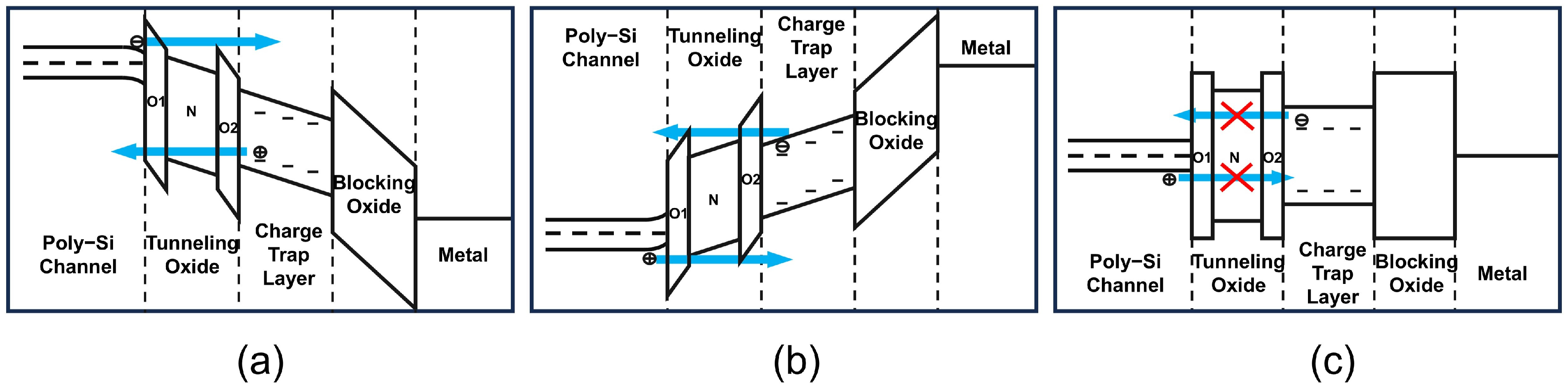
:1. Introduction
2. Materials and Methods
3. Results and Discussion
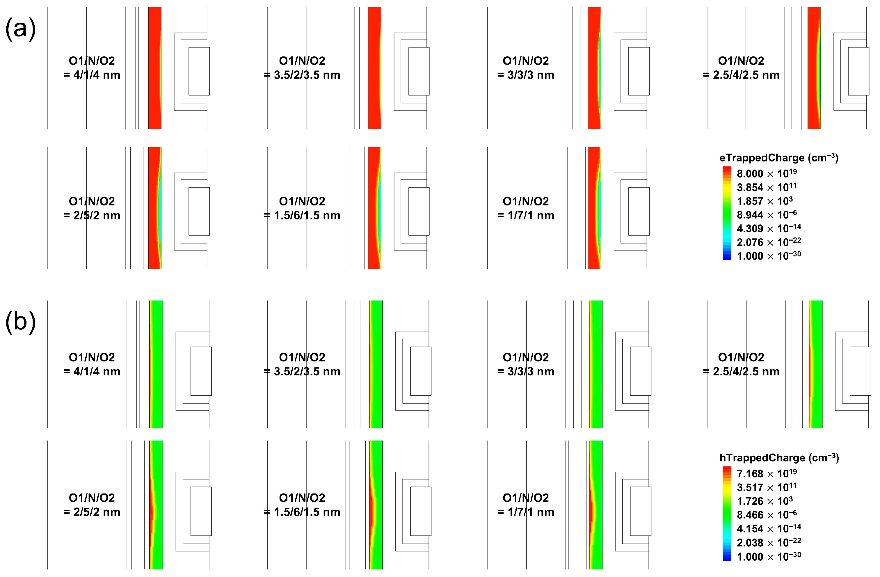
3.1. Effect of N Layer Thickness Variation on Device Performance in O-N-O Architecture
3.1.1. Performance Analysis of Program and Erase Speed
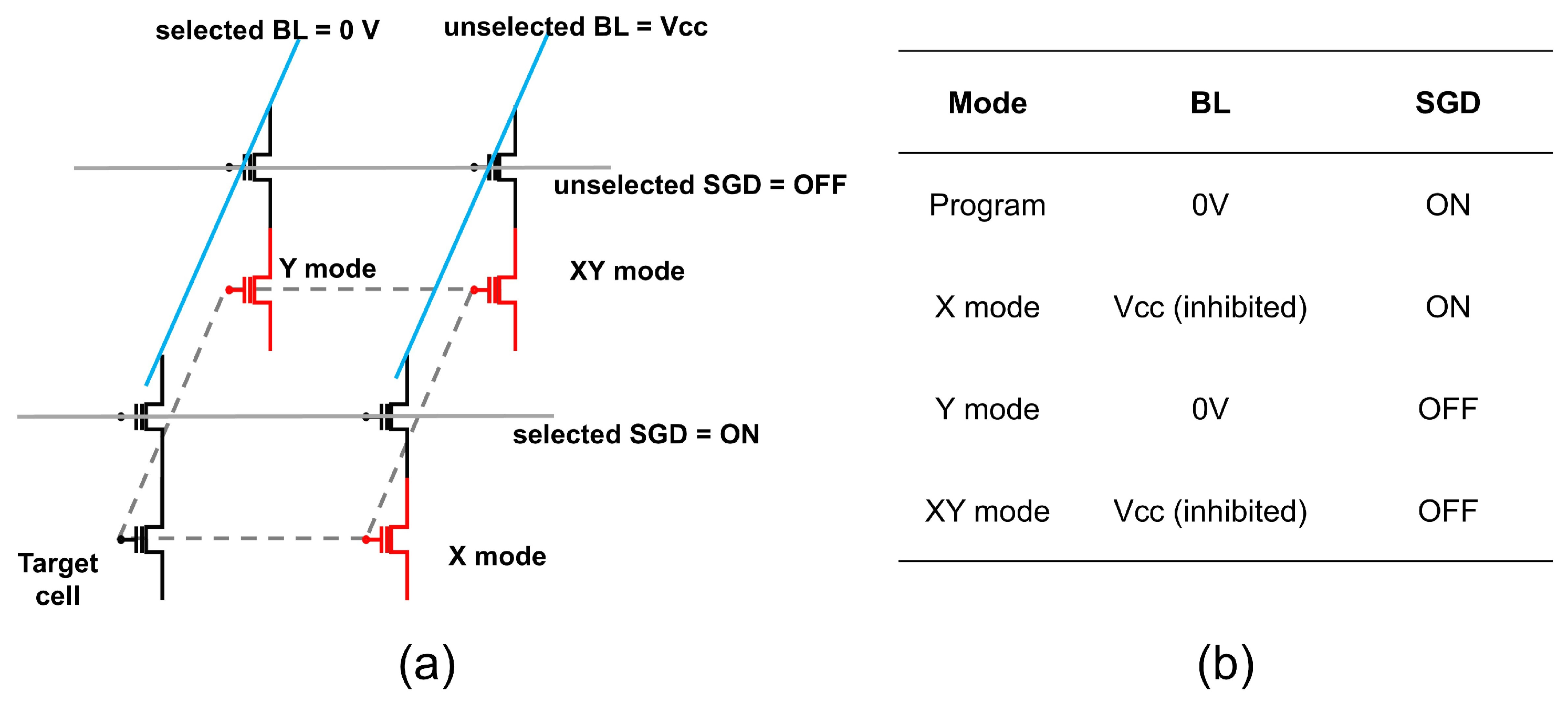
3.1.2. Reliability Analysis of Data Retention and Program Disturb
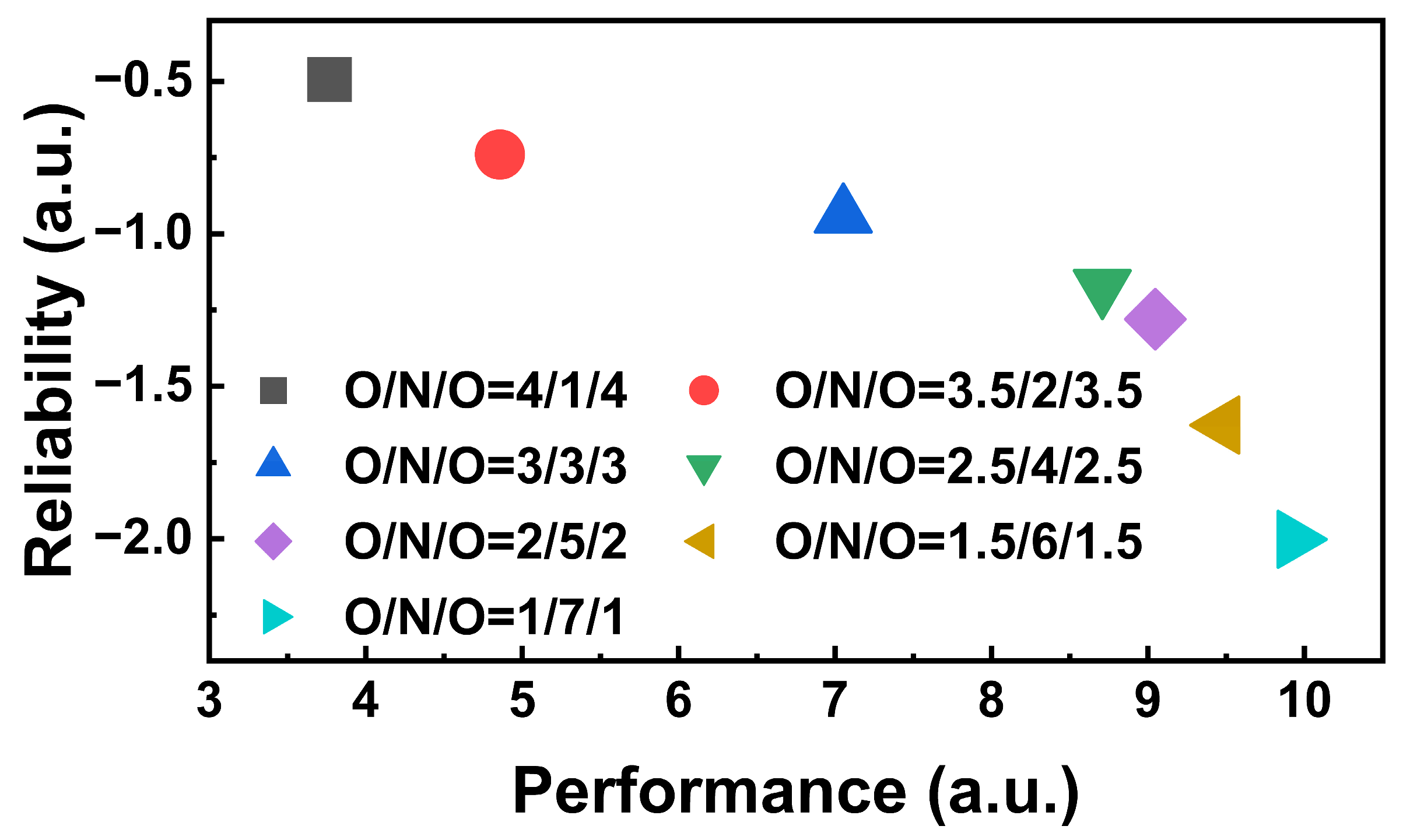
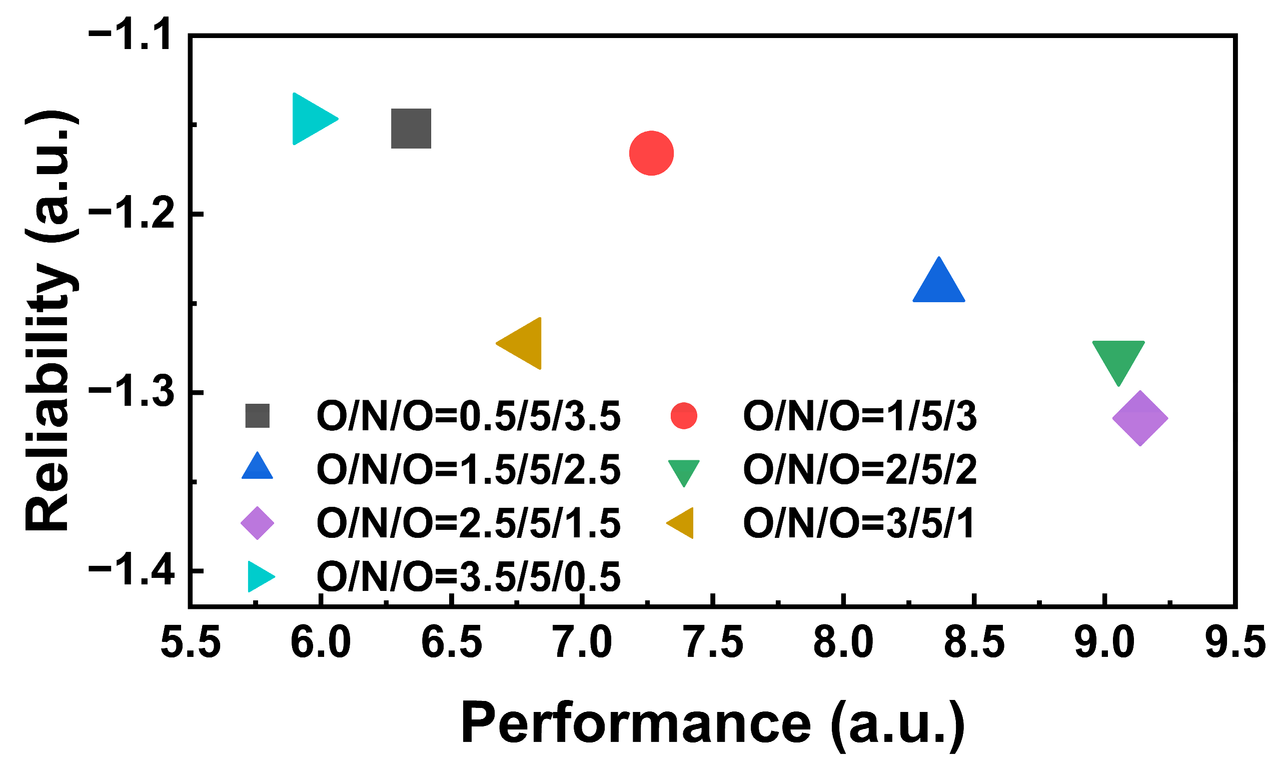
3.2. Optimization of O1 and O2 Layer Thickness for Enhancing Performance
4. Conclusions
Author Contributions
Funding
Data Availability Statement
Conflicts of Interest
References
- Kim, S.S.; Yong, S.K.; Kim, W.; Kang, S.; Park, H.W.; Yoon, K.J.; Sheen, D.S.; Lee, S.; Hwang, C.S. Review of Semiconductor Flash Memory Devices for Material and Process Issues. Adv. Mater. 2023, 35, 2200659. [Google Scholar] [CrossRef]
- Kim, B.; Lee, S.; Hah, B.; Park, K.; Park, Y.; Jo, K.; Noh, Y.; Seol, H.; Lee, H.; Shin, J.; et al. 28.2 A High-Performance 1Tb 3b/Cell 3D-NAND Flash with a 194MB/s Write Throughput on over 300 Layers. In Proceedings of the 2023 IEEE International Solid-State Circuits Conference (ISSCC), San Francisco, CA, USA, 19–23 February 2023; pp. 27–29. [Google Scholar]
- Monzio Compagnoni, C.; Goda, A.; Spinelli, A.S.; Feeley, P.; Lacaita, A.L.; Visconti, A. Reviewing the Evolution of the NAND Flash Technology. Proc. IEEE 2017, 105, 1609–1633. [Google Scholar] [CrossRef]
- Chung, S.S.; Chiang, P.-Y.; Chou, G.; Huang, C.-T.; Chen, P.; Chu, C.-H.; Hsu, C.C.-H. A Novel Leakage Current Separation Technique in a Direct Tunneling Regime Gate Oxide SONOS Memory Cell. In Proceedings of the IEEE International Electron Devices Meeting 2003, Washington, DC, USA, 8–10 December 2003; pp. 26.6.1–26.6.4. [Google Scholar]
- Vianello, E.; Driussi, F.; Palestri, P.; Arreghini, A.; Esseni, D.; Selmi, L.; Akil, N.; van Duuren, M.; Golubovic, D.S. Impact of the Charge Transport in the Conduction Band on the Retention of Si-Nitride Based Memories. In Proceedings of the ESSDERC 2008 —38th European Solid-State Device Research Conference, Scotland, UK, 15–19 September 2008; pp. 107–110. [Google Scholar]
- Goda, A. Recent Progress on 3D NAND Flash Technologies. Electronics 2021, 10, 3156. [Google Scholar] [CrossRef]
- Lue, H.-T.; Lai, S.-C.; Hsu, T.-H.; Du, P.-Y.; Wang, S.-Y.; Hsieh, K.-Y.; Liu, R.; Lu, C.-Y. Modeling of Barrier-Engineered Charge-Trapping Nand Flash Devices. IEEE Trans. Device Mater. Reliab. 2010, 10, 222–232. [Google Scholar] [CrossRef]
- Lue, H.-T.; Wang, S.-Y.; Lai, E.-K.; Hsieh, K.-Y.; Liu, R.; Lu, C.Y. A BE-SONOS (Bandgap Engineered SONOS) NAND for Post-Floating Gate Era Flash Memory. In Proceedings of the 2007 International Symposium on VLSI Technology, Systems and Applications (VLSI-TSA), Hsinchu, Taiwan, 23–25 April 2007; pp. 1–2. [Google Scholar]
- Lue, H.-T.; Wang, S.-Y.; Lai, E.-K.; Shih, Y.-H.; Lai, S.-C.; Yang, L.-W.; Chen, K.-C.; Ku, J.; Hsieh, K.-Y.; Liu, R.; et al. BE-SONOS: A Bandgap Engineered SONOS with Excellent Performance and Reliability. In Proceedings of the IEEE International Electron Devices Meeting, 2005. IEDM Technical Digest, Washington, DC, USA, 5–7 December 2005; pp. 547–550. [Google Scholar]
- Lai, S.-C.; Lue, H.-T.; Yang, M.-J.; Hsieh, J.-Y.; Wang, S.-Y.; Wu, T.-B.; Luo, G.-L.; Chien, C.-H.; Lai, E.-K.; Hsieh, K.-Y.; et al. MA BE-SONOS: A Bandgap Engineered SONOS Using Metal Gate and Al2O3 Blocking Layer to Overcome Erase Saturation. In Proceedings of the 2007 22nd IEEE Non-Volatile Semiconductor Memory Workshop, Monterey, CA, USA, 26–30 August 2007; pp. 88–89. [Google Scholar]
- Liao, J.-H.; Hsieh, J.-Y.; Lue, H.-T.; Yang, L.-W.; Yang, T.; Chen, K.-C.; Lu, C.Y. Performance and Reliability Optimizations of BE-SONOS NAND Flash Using SiON Bandgap-Tuning Tunneling Barrier. In Proceedings of the 2010 IEEE International Reliability Physics Symposium, Anaheim, CA, USA, 2–6 May 2010; pp. 639–643. [Google Scholar]
- Wang, S.-Y.; Lue, H.-T.; Hsu, T.-H.; Du, P.-Y.; Lai, S.-C.; Hsiao, Y.-H.; Hong, S.-P.; Wu, M.-T.; Hsu, F.-H.; Lian, N.-T.; et al. A High-Endurance (≫100K) BE-SONOS NAND Flash with a Robust Nitrided Tunnel Oxide/Si Interface. In Proceedings of the 2010 IEEE International Reliability Physics Symposium, Anaheim, CA, USA, 2–6 May 2010; pp. 951–955. [Google Scholar]
- Kim, M.; Shin, H. Analysis and Compact Modeling of Fast Detrapping from Bandgap-Engineered Tunneling Oxide in 3-D NAND Flash Memories. IEEE Trans. Electron Devices 2021, 68, 3339–3345. [Google Scholar] [CrossRef]
- Cho, T.; Jung, S.; Kang, M. Channel Potential of Bandgap-Engineered Tunneling Oxide (BE-TOX) in Inhibited 3D NAND Flash Memory Strings. Electronics 2024, 13, 1573. [Google Scholar] [CrossRef]
- Yoon, G.; Ko, D.; Park, J.; Kim, D.; Kim, J.; Lee, J.-S. Impact of P/E Stress on Trap Profiles in Bandgap-Engineered Tunneling Oxide of 3D NAND Flash Memory. IEEE Access 2022, 10, 62423–62428. [Google Scholar] [CrossRef]
- Ouyang, Y.; Xia, Z.; Yang, T.; Shi, D.; Zhou, W.; Huo, Z. Optimization of Performance and Reliability in 3D NAND Flash Memory. IEEE Electron Device Lett. 2020, 41, 840–843. [Google Scholar] [CrossRef]
- Van den Bosch, G.; Kar, G.S.; Blomme, P.; Arreghini, A.; Cacciato, A.; Breuil, L.; De Keersgieter, A.; Paraschiv, V.; Vrancken, C.; Douhard, B.; et al. Highly Scaled Vertical Cylindrical SONOS Cell With Bilayer Polysilicon Channel for 3-D Nand Flash Memory. IEEE Electron Device Lett. 2011, 32, 1501–1503. [Google Scholar] [CrossRef]
- Lue, H.-T.; Shih, Y.-H.; Hsieh, K.-Y.; Liu, R.; Lu, C.-Y. A Transient Analysis Method to Characterize the Trap Vertical Location in Nitride-Trapping Devices. IEEE Electron Device Lett. 2004, 25, 816–818. [Google Scholar] [CrossRef]
- Park, K.-T.; Nam, S.; Kim, D.; Kwak, P.; Lee, D.; Choi, Y.-H.; Choi, M.-H.; Kwak, D.-H.; Kim, D.-H.; Kim, M.-S.; et al. Three-Dimensional 128 Gb MLC Vertical Nand Flash Memory With 24-WL Stacked Layers and 50 MB/s High-Speed Programming. IEEE J. Solid-State Circuits 2015, 50, 204–213. [Google Scholar] [CrossRef]
- Jang, J.; Kim, H.-S.; Cho, W.; Cho, H.; Kim, J.; Shim, S.I.; Younggoan; Jeong, J.-H.; Son, B.-K.; Kim, D.W.; et al. Vertical Cell Array Using TCAT (Terabit Cell Array Transistor) Technology for Ultra High Density NAND Flash Memory. In Proceedings of the 2009 Symposium on VLSI Technology, Kyoto, Japan, 15–17 June 2009; pp. 192–193. [Google Scholar]
- Hemink, G.; Goda, A. 5-NAND Flash Technology Status and Perspectives. In Semiconductor Memories and Systems; Redaelli, A., Pellizzer, F., Eds.; Woodhead Publishing Series in Electronic and Optical Materials; Woodhead Publishing: Cambridge, UK, 2022; pp. 119–158. ISBN 978-0-12-820758-1. [Google Scholar]
- Nam, K.; Park, C.; Yoon, J.-S.; Jang, H.; Park, M.S.; Sim, J.; Baek, R.-H. Origin of Incremental Step Pulse Programming (ISPP) Slope Degradation in Charge Trap Nitride Based Multi-Layer 3D NAND Flash. Solid State Electron. 2021, 175, 107930. [Google Scholar] [CrossRef]
- Cuevas, A.; Stocks, M.; McDonald, D.; Kerr, M.; Samundsett, C. Recombination and Trapping in Multicrystalline Silicon. IEEE Trans. Electron Devices 1999, 46, 2026–2034. [Google Scholar] [CrossRef]
- Southwick, R.G.; Reed, J.; Buu, C.; Butler, R.; Bersuker, G.; Knowlton, W.B. Limitations of Poole–Frenkel Conduction in Bilayer HfO2/SiO2 MOS Devices. IEEE Trans. Device Mater. Reliab. 2010, 10, 201–207. [Google Scholar] [CrossRef]
- Swain, R.; Jena, K.; Lenka, T.R. Modeling of Forward Gate Leakage Current in MOSHEMT Using Trap-Assisted Tunneling and Poole–Frenkel Emission. IEEE Trans. Electron Devices 2016, 63, 2346–2352. [Google Scholar] [CrossRef]
- Ieong, M.; Solomon, P.M.; Laux, S.E.; Wong, H.-S.P.; Chidambarrao, D. Comparison of Raised and Schottky Source/Drain MOSFETs Using a Novel Tunneling Contact Model. In Proceedings of the International Electron Devices Meeting 1998. Technical Digest (Cat. No.98CH36217), San Francisco, CA, USA, 6–9 December 1998; pp. 733–736. [Google Scholar]
- Yoon, G.; Go, D.; Park, J.; Kim, D.; Kim, J.; An, U.; Kim, J.; Lee, J.-S.; Kong, B.D. Impact of Electron and Hole Trap Profiles in BE-TOX on Retention Characteristics of 3D NAND Flash Memory. IEEE Trans. Nanotechnol. 2024, 23, 733–740. [Google Scholar] [CrossRef]
- Lenzlinger, M.; Snow, E.H. Fowler-Nordheim Tunneling into Thermally Grown SiO2. J. Appl. Phys. 1969, 40, 278–283. [Google Scholar] [CrossRef]
- Salace, G.; Hadjadj, A.; Petit, C.; Jourdain, M. Temperature Dependence of the Electron Affinity Difference between Si and SiO2 in Polysilicon (N+)–Oxide–Silicon (p) Structures: Effect of the Oxide Thickness. J. Appl. Phys. 1999, 85, 7768–7773. [Google Scholar] [CrossRef]
- Siau, C.; Kim, K.-H.; Lee, S.; Isobe, K.; Shibata, N.; Verma, K.; Ariki, T.; Li, J.; Yuh, J.; Amarnath, A.; et al. 13.5 A 512Gb 3-Bit/Cell 3D Flash Memory on 128-Wordline-Layer with 132MB/s Write Performance Featuring Circuit-Under-Array Technology. In Proceedings of the 2019 IEEE International Solid-State Circuits Conference (ISSCC), San Francisco, CA, USA, 17–21 February 2019; pp. 218–220. [Google Scholar]
- Komori, Y.; Kido, M.; Kito, M.; Katsumata, R.; Fukuzumi, Y.; Tanaka, H.; Nagata, Y.; Ishiduki, M.; Aochi, H.; Nitayama, A. Disturbless Flash Memory Due to High Boost Efficiency on BiCS Structure and Optimal Memory Film Stack for Ultra High Density Storage Device. In Proceedings of the 2008 IEEE International Electron Devices Meeting, San Francisco, CA, USA, 15–17 December 2008; pp. 1–4. [Google Scholar]
- Fukuzumi, Y.; Katsumata, R.; Kito, M.; Kido, M.; Sato, M.; Tanaka, H.; Nagata, Y.; Matsuoka, Y.; Iwata, Y.; Aochi, H.; et al. Optimal Integration and Characteristics of Vertical Array Devices for Ultra-High Density, Bit-Cost Scalable Flash Memory. In Proceedings of the 2007 IEEE International Electron Devices Meeting, Washington, DC, USA, 10–12 December 2007; pp. 449–452. [Google Scholar]
- Hsu, T.-H.; Lue, H.-T.; Du, P.-Y.; Chen, W.-C.; Yeh, T.-H.; Lo, R.; Chang, H.-S.; Wang, K.-C.; Lu, C.-Y. Study of Self-Healing 3D NAND Flash with Micro Heater to Improve the Performances and Lifetime for Fast NAND in NVDIMM Applications. In Proceedings of the 2019 IEEE 11th International Memory Workshop (IMW), Monterey, CA, USA, 12–15 May 2019; pp. 1–4. [Google Scholar]
- Choi, S.; Choi, C.; Jeong, J.K.; Song, Y.-H. Innovative Structure to Improve Erase Speed in 3-D Nand Flash Memory with Cell-on-Peri (COP) Applied. IEEE Trans. Electron Devices 2022, 69, 4883–4888. [Google Scholar] [CrossRef]
- Keister, J.W.; Rowe, J.E.; Kolodziej, J.J.; Niimi, H.; Madey, T.E.; Lucovsky, G. Band Offsets for Ultrathin SiO2 and Si3N4 Films on Si (111) and Si (100) from Photoemission Spectroscopy. J. Vac. Sci. Technol. B Microelectron. Nanometer Struct. Process. Meas. Phenom. 1999, 17, 1831–1835. [Google Scholar] [CrossRef]
- Miyazaki, S. Photoemission Study of Energy-Band Alignments and Gap-State Density Distributions for High-k Gate Dielectrics. J. Vac. Sci. Technol. B Microelectron. Nanometer Struct. Process. Meas. Phenom. 2001, 19, 2212–2216. [Google Scholar] [CrossRef]
- Sorokin, A.N.; Karpushin, A.A.; Gritsenko, V.A.; Wong, H. Electronic Structure of Amorphous Silicon Oxynitride with Different Compositions. J. Appl. Phys. 2009, 105, 073706. [Google Scholar] [CrossRef]
- Shim, K.S.; Choi, E.S.; Jung, S.W.; Kim, S.H.; Yoo, H.S.; Jeon, K.S.; Hong, S.J. Inherent Issues and Challenges of Program Disturbance of 3D NAND Flash Cell. In Proceedings of the 2012 4th IEEE International Memory Workshop, Milan, Italy, 20–23 May 2012; pp. 1–4. [Google Scholar]
- Choi, E.-S.; Park, S.-K. Device Considerations for High Density and Highly Reliable 3D NAND Flash Cell in near Future. In Proceedings of the 2012 International Electron Devices Meeting, San Francisco, CA, USA, 10–13 December 2012; pp. 9.4.1–9.4.4. [Google Scholar]
- Yoo, H.; Choi, E.; Oh, J.; Park, K.; Jung, S.; Kim, S.; Shim, K.; Joo, H.; Jeon, K.; Seo, M.; et al. Modeling and Optimization of the Chip Level Program Disturbance of 3D NAND Flash Memory. In Proceedings of the 2013 5th IEEE International Memory Workshop, Monterey, CA, USA, 26–29 May 2013; pp. 147–150. [Google Scholar]
- Kang, M.; Kim, Y. Natural Local Self-Boosting Effect in 3D NAND Flash Memory. IEEE Electron Device Lett. 2017, 38, 1236–1239. [Google Scholar] [CrossRef]


| Parameters | Value (nm) |
|---|---|
| Thickness of core filler (Tcore) | 15 |
| Thickness of polysilicon channel (Tchannel) | 15 |
| Thickness of the first SiO2 tunneling layer (TO1) | 4/3.5/3/2.5/2/1.5/1/0.5 |
| Thickness of the SiOxNy tunneling layer (TN) | 1/2/3/4/5/6/7 |
| Thickness of the second SiO2 tunneling layer (TO2) | 4/3.5/3/2.5/2/1.5/1/0.5 |
| Thickness of charge-trapping layer (TCTL) | 7 |
| Thickness of SiO2 blocking oxide layer (TBO) | 8 |
| Thickness of Al2O3 layer (TA) | 4 |
| Thickness of TiN layer (TTi) | 3 |
| Thickness of tungsten gate (TW) | 8 |
| Length of the word line (Lw) | 30 |
| Length of the spacing between word lines (Ls) | 30 |
Disclaimer/Publisher’s Note: The statements, opinions and data contained in all publications are solely those of the individual author(s) and contributor(s) and not of MDPI and/or the editor(s). MDPI and/or the editor(s) disclaim responsibility for any injury to people or property resulting from any ideas, methods, instructions or products referred to in the content. |
© 2025 by the authors. Licensee MDPI, Basel, Switzerland. This article is an open access article distributed under the terms and conditions of the Creative Commons Attribution (CC BY) license (https://creativecommons.org/licenses/by/4.0/).
Share and Cite
Xu, Z.; Xie, S.; Ying, Z.; Zhang, W.; Gao, L. Modeling and Optimization of Structural Tuning in Bandgap-Engineered Tunneling Oxide for 3D NAND Flash Application. Electronics 2025, 14, 1461. https://doi.org/10.3390/electronics14071461
Xu Z, Xie S, Ying Z, Zhang W, Gao L. Modeling and Optimization of Structural Tuning in Bandgap-Engineered Tunneling Oxide for 3D NAND Flash Application. Electronics. 2025; 14(7):1461. https://doi.org/10.3390/electronics14071461
Chicago/Turabian StyleXu, Zhihong, Shibo Xie, Zhijun Ying, Wenlong Zhang, and Liming Gao. 2025. "Modeling and Optimization of Structural Tuning in Bandgap-Engineered Tunneling Oxide for 3D NAND Flash Application" Electronics 14, no. 7: 1461. https://doi.org/10.3390/electronics14071461
APA StyleXu, Z., Xie, S., Ying, Z., Zhang, W., & Gao, L. (2025). Modeling and Optimization of Structural Tuning in Bandgap-Engineered Tunneling Oxide for 3D NAND Flash Application. Electronics, 14(7), 1461. https://doi.org/10.3390/electronics14071461