Article

An Innovative Digital Pulse Width Modulator and Its Field-Programmable Gate Array Implementation

Department of Information Engineering (DEI), University of Padova, 35131 Padova, Italy
Electronics 2025, 14(8), 1522; https://doi.org/10.3390/electronics14081522
Submission received: 28 February 2025 / Revised: 1 April 2025 / Accepted: 2 April 2025 / Published: 9 April 2025
(This article belongs to the Special Issue Emerging Applications of FPGAs and Reconfigurable Computing System)

Abstract

:
Digital pulse-width modulation (DPWM)-based controls are characterized by a non-negligible phase delay due to analog-to-digital (ADC) conversion, sampling time, carrier shape, and algorithm computation time. These delays degrade the performance in closed-loop systems, where the bandwidth must be reduced to avoid instability issues due to the reduced closed-loop phase margin. To mitigate these delays, approaches such as utilizing low-latency ADCs or increasing the sampling frequency have been employed. However, these methods are often costly and do not address the fundamental delay issues inherent to DPWMs. In this paper, a novel zero phase-delay DPWM architecture is proposed. This enhanced architecture seamlessly integrates pulse width and frequency modulation to create a programmable derivative action, capable of effectively recovering the DPWM delay. The proposed architecture employs a reliable and straightforward organization, suitable for implementation in commercial field programmable gate array (FPGA). Furthermore, this architecture inherently generates a trigger signal that can be used in numerous power electronic applications to capture the average value in piecewise linear inductor currents. The validity of the proposed architecture is substantiated through simulations and experimental tests. The final implementation is shared in an open-source resource.

1. Introduction

Digital pulse width modulators (DPWMs) are widely used in power electronics applications due to their low cost, low power consumption, and ease of use [1,2,3,4,5]. However, digital PWMs suffer from phase delays that limit their dynamic performance, particularly at high frequencies. Despite these limitations, there are many reasons to use digital controls. The main motivations for their development include enhanced safety and monitoring functions, robustness against parametric variations and component degradation, as well as programmability and the possibility of modifying the control scheme after deployment. Digital controls offer the advantage of being re-programmable and re-configurable, enabling the implementation of controllers that may be difficult or even unfeasible in the analog domain [6,7,8]. However, in terms of dynamic performance, analog controllers still provide superior bandwidth. Several strategies have been proposed in the literature to mitigate the inherent delays of digital control systems [4,9,10,11,12,13], yet phase delay remains a critical issue and is often compensated for elsewhere in the system [14].
To reduce the performance gap between digital PWM and analog PWM, one approach is to increase the number of samples per modulation period [15,16]. However, increasing the sampling rate introduces non-linearities that may lead to severe system failures [17,18]. A promising trade-off is represented by the double-sampling DPWM based on the Trailing-Triangle edge (TTE) carrier. Although this technique mitigates phase lag, it does not entirely eliminate it and may still lead to performance degradation at high switching frequencies.
Other advanced control strategies, such as predictive control, have been explored to improve dynamic response [19,20,21,22]. However, these approaches often involve significant computational complexity, making them difficult to implement in many power electronics applications. As a result, DPWM-based control remains the most widely adopted solution. To date, the only methods capable of compensating for the delays introduced by digital modulators are those presented in [23,24,25]. In [26], the authors apply the zero phase delay architecture to digitally controlled grid-connected converters to extend the high frequency passivity admittance.
This paper introduces a novel digital implementation of a variable-frequency DPWM featuring an intrinsic derivative action. While existing digital architectures are theoretically valid, their practical implementation remains challenging. In contrast, this study proposes a simple yet effective digital architecture. The proposed enhanced DPWM (eDPWM) overcomes the main limitations of previous designs [23,24,25] while also providing a streamlined digital structure that can be efficiently implemented in FPGA or custom digital systems with minimal resource consumption.
The structure of digital modulators based on the asymmetric dual-edge (ADE) carrier is revised and optimized to eliminate complex multiplications and divisions between signals. Furthermore, the enhanced structure inherently generates a synchronization signal that serves as an accurate trigger for ADCs, facilitating the acquisition of the average value of piecewise linear inductor currents in power electronics applications. Such synchronization is not present in conventional ADE-based structures. Throughout this manuscript, DPWM architectures that introduce zero-phase delay or phase boost are collectively referred to as enhanced DPWM (eDPWM).
Currently, eDPWM structures can only be implemented using Field-Programmable Gate Arrays (FPGAs) or custom digital circuits. However, the solutions proposed in [1,2] are computationally intensive, restricting zero-delay modulators to systems with abundant computational resources. This complexity has hindered their widespread adoption. Instead, the proposed structure is designed to be both simple and computationally efficient, eliminating the need for bidirectional counters, as required in TTE-based architectures. This approach allows the full utilization of the available numerical resolution without compromising precision [27].
Basic concepts of digital control for power electronics can be found in [6], while their efficient FPGA implementation is thoroughly discussed in [28]. However, both references focus on digital control implementations using constant-frequency DPWM. This paper aims to bridge this gap by introducing an architecture that enables the implementation of eDPWM in a straightforward and reliable manner.
The main contributions of this paper are listed as follows.
  • A new DPWM (eDPWM) with zero phase delay or a programmable derivative action is proposed.
  • The overall DPWM architecture complexity is simplified and relaxed. Indeed, in the architecture in [23], the derivative action is achieved by changing the values of a and b. This implies that the comparator slopes must be modified according to the values of a and b. Counting with programmable slopes overcomplicates the counter implementation. The new architecture eradicates the use of products between signals to achieve the derivative action and the DPWM counters always count with a constant slope (i.e., the ratio T smpl / T s is constant). This greatly simplified the programmability of the derivative action and the overall architecture.
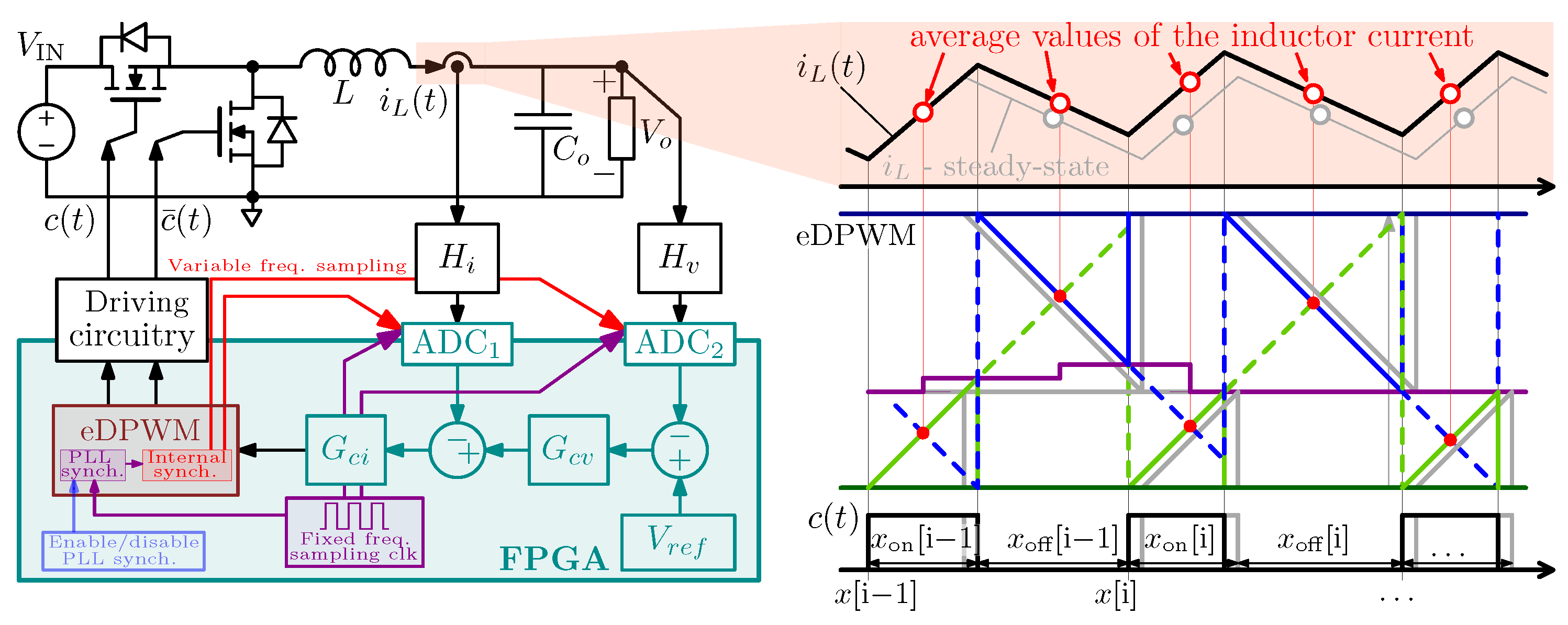
  • The synchronism mechanism is greatly simplified. Indeed, the eDPWM intrinsically provides the instant corresponding to the middle of the ON and OFF phases. As required in countless digital controls for power electronic applications, such a signal triggers the ADC sampling to acquire the average value of piecewise linear signals. This trigger event is not intrinsically present in ADE-DPWM; adding it increases the system complexity, as shown in [24,25]. Conversely, in the eDPWM, the synchronism mechanism can be easily implemented using the aforementioned trigger signal without further increasing the architecture’s complexity.
  • The DPWM architecture is optimized to use all available bits. Namely, since the comparator slopes are fixed and proportional to the T smpl / T s ratio, and since they must always count in one direction (i.e., up-count or down-count), the resolution of the DPWM can be increased to make maximum use of all available bits, even doing better than the TTE-DPWM in which one bit is lost due to alternating up-count and down-count.
  • Other original contributions in this article are the block diagram of ADE-DPWM modulators and other alternative implementations of eDPWMmodulators.
The remainder of the paper is organized as follows. Section 2 compares the state-of-the-art double-sampling TTE carrier-based DPWM (TTE-DPWM) with the double-sampling ADE carrier-based DPWM (ADE-DPWM), introduces the main concepts of variable-frequency DPWM, and presents a preliminary architecture for eDPWM. Section 3 derives the final architecture of eDPWM. Section 4 demonstrates the equivalence between the proposed eDPWM and the ADE-DPWM presented in [23]. The small signal model is subsequently derived. Section 5 presents the experimental results validating the proposed architecture. Finally, Section 6 concludes the manuscript by summarizing the main contributions.

2. Enhanced DPWM: Main Concepts

This manuscript introduces an enhanced double-sampling DPWM architecture designed to eliminate the delays typically associated with classical digital modulators while maintaining a simple and efficient implementation. These modulators were first proposed in [23,24,25], where the asymmetric dual-edge (ADE) carrier is introduced to enhance the frequency response. Specifically, ADE carrier-based DPWM (ADE-DPWM) demonstrated its ability to fully recover the phase delay associated with classical DPWM structures and, in some cases, provide a derivative action that guarantees a high-frequency phase boost.
To establish a clear understanding of the fundamental differences between traditional fixed-frequency DPWMs and variable-frequency architectures, this section begins with a comparative analysis of Trailing-Triangle Edge DPWM (TTE-DPWM) and ADE-DPWM. This comparison not only illustrates the core operating principles of ADE-DPWM but also highlights its critical distinctions from conventional digital modulators.

2.1. Fixed-Frequency vs. Variable-Frequency DPWM Architectures

A fundamental limitation of fixed-frequency DPWM architectures is the inherent phase delay introduced by the discrete-time processing of the modulating signal. In particular, single-sampling TTE-DPWM exhibits a phase delay that can described by the following transfer function
G TTE , single ( s ) = 1 2 e s T s x off 2 + e s T s x on 2 ,
where s C is the complex variable of the Laplace plane. The phase response can be approximated by G TTE , double ( s ) e s T s 2 . The introduction of double-sampling DPWM reduces this delay, yielding G TTE , double ( s ) e S · T s / 4 .
While increasing the sampling frequency further decreases the phase lag, it never fully eliminates it. Moreover, attempting to sample more than twice per period introduces additional non-idealities [15,16]. In contrast, variable-frequency DPWM architectures, such as ADE-DPWM, dynamically adjust the switching period based on the modulating signal. This enables complete phase delay cancellation, making ADE-DPWM particularly effective for high-bandwidth control applications. However, this benefit comes at the cost of increased implementation complexity. To elucidate the fundamental principles governing the operation of the double-sampling ADE-DPWM and to delineate its salient distinctions from the state-of-the-art TTE-DPWM, a comparative analysis between these two architectures is reported in the following.
Figure 1 shows a comparison between the TTE-DPWM and the ADE-DPWM as proposed in [25]. Both the x and y axes are normalized. The main difference between the two architectures lies in the modulation of the switching period. Indeed, the TTE-DPWM operates with a constant frequency, while the ADE-DPWM introduces a frequency modulation. This effect can be formalized as follows.
When the modulating signal M [ · ] increases, all DPWM systems react by increasing the ON phase while decreasing the OFF phase. In double-sampling TTE-DPWM, once fixed x on-TTE [ i ] = T on-TTE [ i ] T s , the OFF phase is imposed by the relation T on-TTE [ i ] + T off-TTE [ i ] = T s = constant . On the other hand, ADE-DPWM allows independent changes in both ON and OFF phases. With a positive variation of M [ · ] , the modulation period decreases (i.e., T s [ i ] < T s ), and therefore x on [ i ] = T on-ADE [ i ] T s [ i ] > T on-ADE [ i ] T s . Furthermore T on-ADE [ i ] > T on-TTE [ i ] and therefore x on-ADE [ i ] > x on-TTE [ i ] . Having reduced the modulation period, one also obtains T off-ADE [ i ] = T s-ADE [ i ] T on-ADE [ i ] < T s T on-TTE [ i ] . Thus, for the same modulating signal variation, the ADE-DPWM reacts with more pronounced variations of ON and OFF phases. Moreover, these variations are independent and their sum is not constant thus leading to a modulation of the switching period.
Analytically, one has
ADE : Δ x on-ADE [ i ] = Δ M on [ i ] Δ x off-ADE [ i ] = Δ M off [ i ] Δ x s-ADE [ i ] = Δ M on [ i ] Δ M off [ i ] ; TTE : Δ x on-TTE [ i ] = Δ M on [ i ] + Δ M off [ i ] 2 Δ x off-TTE [ i ] = Δ M on [ i ] + Δ M off [ i ] 2 Δ x s-TTE [ i ] = 0 ,
with
Δ x s ADE [ i ] T s ADE [ i ] T s T s , Δ x s TTE [ i ] T s TTE [ i ] T s T s ,
while Δ x on-TTE [ i ] and Δ x off-TTE [ i ] are the normalized variations of the ON and OFF phases for the TTE-DPWM.
Equation (2) indicates that the most important characteristic of the double-sampling ADE-DPWM is the switching frequency modulation. But at this point, one might wonder whether the rather complex structure of the ADE architecture could not be simplified. The next section introduces changes in the overall structure that induce the same time domain operation. The new architecture organization is therefore extended in order to emulate even the more complex architecture proposed in [23].

2.2. Challenges in ADE-DPWM Implementation

Although ADE-DPWM eliminates phase delay, its practical implementation is hindered by the following challenges.
  • Computational complexity: ADE-DPWM requires real-time multiplications and divisions, significantly increasing hardware resource utilization.
  • Synchronization issues: Unlike fixed-frequency DPWM, ADE-DPWM lacks an intrinsic sampling synchronization mechanism, making accurate current measurement more challenging.
  • Hardware limitations: ADE-DPWM is difficult to implement on FPGAs and is impossible to realize on microcontrollers due to excessive computational demands.
These challenges motivate the development of an improved structure that preserves the advantages of ADE-DPWM while simplifying implementation.

2.3. Proposed eDPWM Architecture

To overcome the limitations of ADE-DPWM, the enhanced DPWM (eDPWM) is proposed. This new architecture retains the double-sampling and variable-frequency properties of ADE-DPWM but introduces fundamental modifications that make it computationally efficient and easier to implement. The core differences between TTE-DPWM, ADE-DPWM, and eDPWM architectures are summarized in Table 1.
The first version of the eDPWM, hereafter referred to as eDPWM v1.0, is illustrated in Figure 2. This structure replicates the same time domain operation of ADE-DPWM but avoids unnecessary arithmetic operations, leading to a drastic reduction in computational requirements.
Assuming that all the carrier slopes S of the eDPWM are equal (i.e., the up-count slope and the down-count slope are equal), and by indicating with M on [ i ] and M off [ i ] the values of the modulating signal acquired (sampled) at the middle of the ON and OFF phases, it is easy to verify the following relationships. For the eDPWM v1.0, the i-th ON and OFF phases duration can be written as follows:
x on [ i ] = M ss S + Δ M on [ i ] S = M ss S + M on [ i ] M ss S = M on [ i ] S ; x off [ i ] = 1 M ss S Δ M off [ i ] S = 1 M ss S M off [ i ] M ss S = 1 M off [ i ] S ,
where Δ M on [ i ] M on [ i ] M ss and Δ M off [ i ] M off [ i ] M ss are the variation of the modulating signal during the i-th ON and OFF phases with respect to the steady state value M ss .
The i-th ON and OFF phases variation can be written as follows:
Δ x on [ i ] x on [ i ] x on = x on [ i ] M ss S = Δ M on [ i ] S , Δ x off [ i ] x off [ i ] x off = 1 M ss S x off [ i ] = Δ M off [ i ] S .
By choosing S = 1 , the time domain operation (5) is the same as the one obtained in [23,24]. The structures described in Figure 2 and Figure 3 lead to the same time domain expressions of that obtained with the double-sampling ADE-DPWM. The main advantages of the proposed structure with respect to the double-sampling ADE-DPWM can be summarized as follows:
  • The carrier counters always start from a constant value. In the ADE carrier-based structure, the starting point of the carrier must be updated at the beginning of each ON and OFF phases.
  • Differently than ADE-DPWM, counting operations to implement the two carriers are uninterrupted. The counter always starts from zero, and the change in the modulating signal is not added to the counter. The only values that must be set are the compare values for the two carriers.
The listed advantages are remarkable. However, further modifications are required to build an efficient and functional architecture. Indeed, despite the improvements, the eDPWM v1.0 structure still has some critical issues. First, two different comparitive values are required for the two ramps. Therefore, each sampling is followed by an operation to calculate the 1 M [ · ] value from the M [ · ] value just acquired. The second problem is related to the synchronism. In many structures, it is necessary to sample the current at precise points such as the one that gets the average value of a piecewise linear waveform. The ADE-DPWM structure and the eDPWM v1.0 structure do not naturally offer such an instant of synchronism. In the next chapter, both problems are solved with the eDPWM v1.5 architecture.

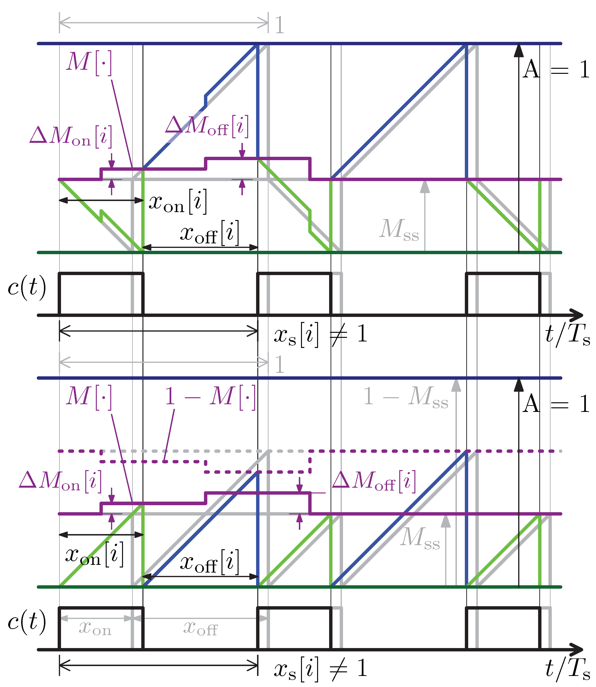
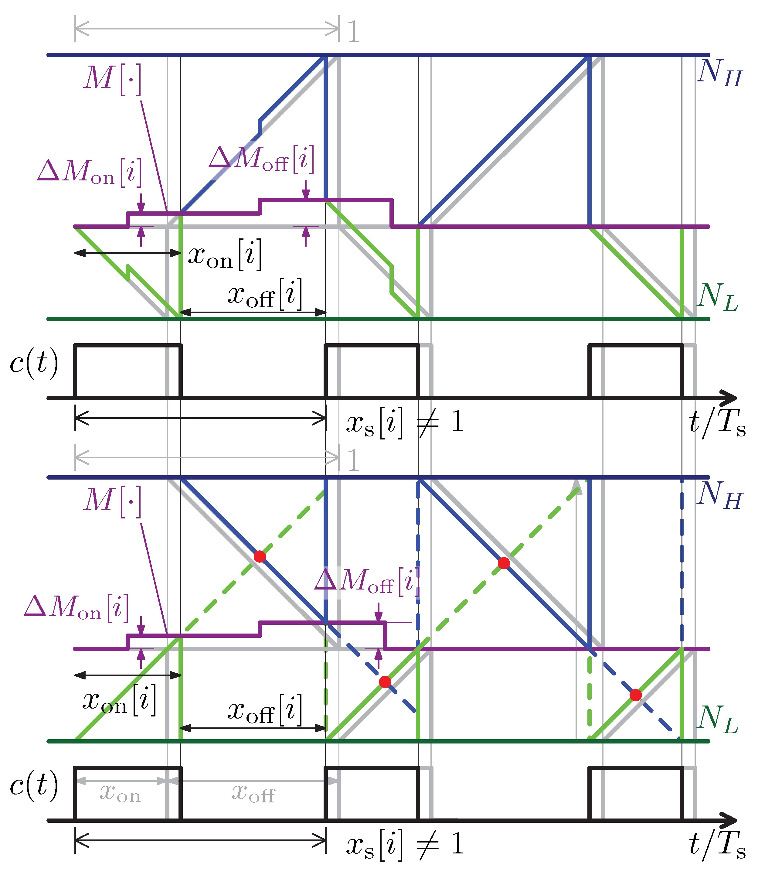
3. General eDPWM Organization

This section presents the final version of the eDPWM modulator.
The eDPWM v1.5 operation is reported in Figure 4. The main differences with respect to that in Figure 3 lie in the carriers organization and the reset mechanism. The blue carrier always starts from its maximum value (i.e., A = 1 ) and down-counts up to the intersection with M [ · ] . The evaluation of the signal 1 M [ · ] is therefore unnecessary.
There are other properties to be exploited in this architectural organization. For example, instead of resetting the ramps immediately after the intersection with the value of the compare register (i.e., M on [ i ] or M off [ i ] ), both ramps are reset in correspondence with the count-start command of the other one. This mechanism, generates an intersection (highlighted by a red dot in the figure) that, in steady-state, represents the central instant of the ON and OFF phases. These instants represent the trigger event of the missing synchronism mentioned in the previous paragraph and are deeply discussed in [24,25]. Section 3.2 clarifies why this mechanism is so relevant. Thus, the eDPWM v1.5 structure solves both residual problems of the eDPWM v1.0 structure.

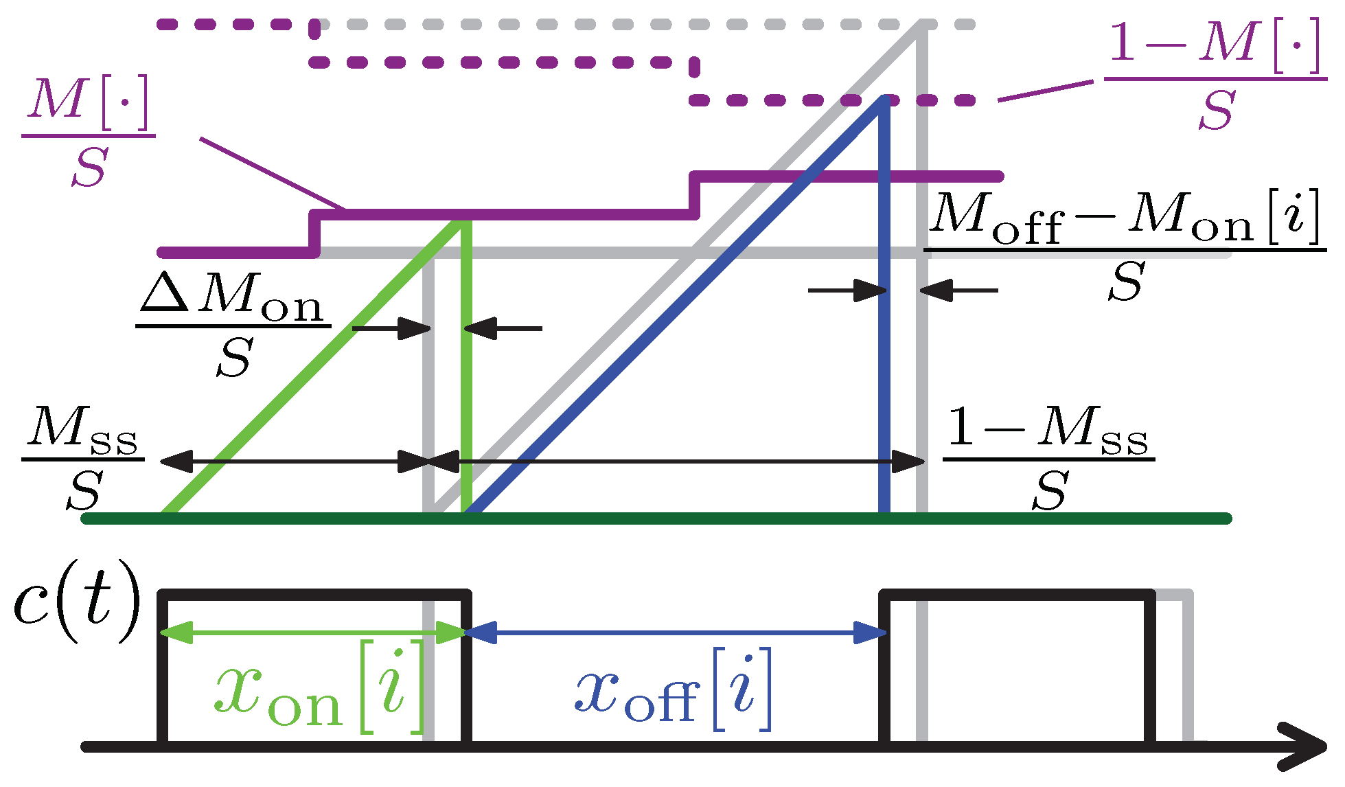
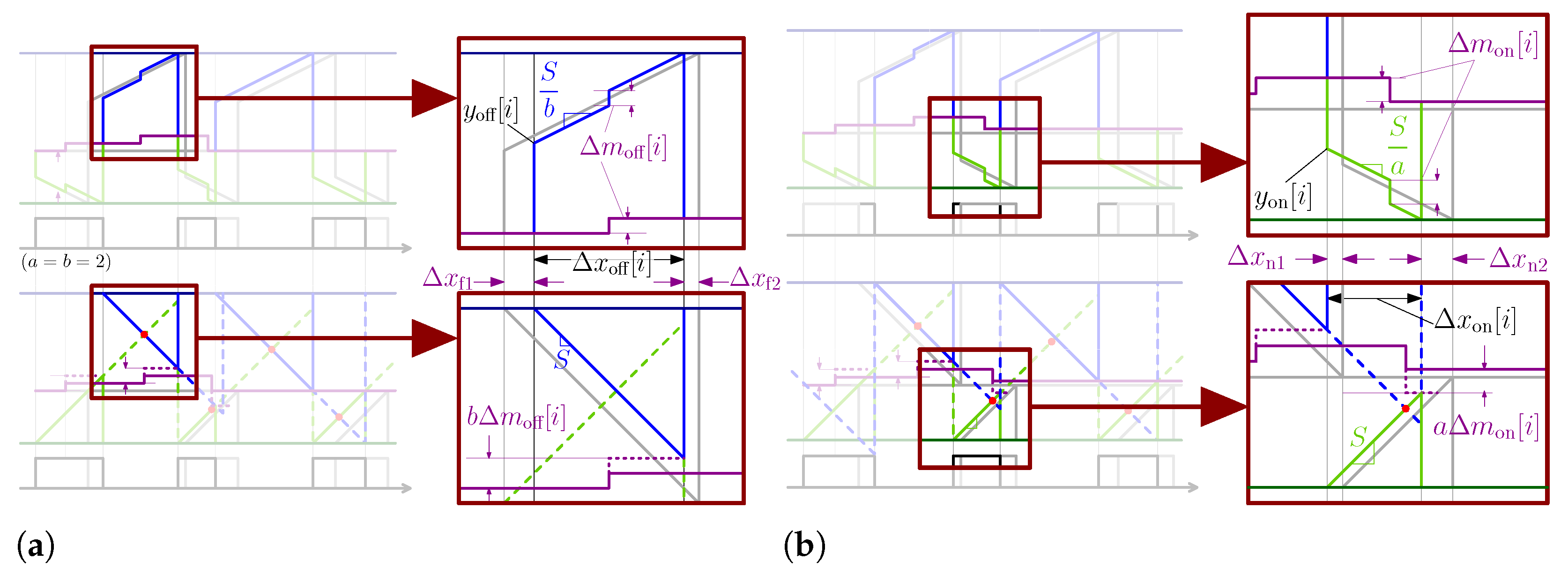
3.1. Intrinsic Programmable Derivative Actions

The structure eDPWM v1.5 is further modified to emulate the DS ADE-DPWM proposed in [23]. Emulating this behavior is important since it adds a programmable high-frequency phase boost. The main issue of the structure in [23] is the complex architecture. For instance, to achieve the programmable derivative action, the modulator proposed in [23] requires to change both counters’ slopes. This is done by dividing them by parameters a , b R . Obtaining programmable counters’ slopes increases the architecture complexity and leads to a significant reduction in the final resolution adopted to represent the modulating signal. Figure 5 shows the comparison between the eDPWM v2.0 and the ADE-DPWM in [23]. The two architectures, operating with the same input, provide the same time response, even during transients. However, there is a huge gap in the architecture complexity of the two architectures even in the simplest case obtained for a = b = 1 . Parameters a , b R are introduced in. In the example reported in Figure 5, the modulating signal is directly passed for comparison with the upper and lower carriers to compute the rising and falling edges of the control signal (i.e., the modulator’s output). In the ADE architecture, even in the simple case for a = b = 1 , several operations must be performed to obtain the control signal. Specifically, one has to perform the sum of two signals, a comparison with the ramps with variable slopes, and then a further product between signals. The situation is even worse when a , b 1 . Indeed, the proposed architecture directly computes the derivative terms a Δ M on [ i ] and b Δ M off [ i ] while ADE-DPWM in [23] requires further sums, multiplications, and divisions to perform the derivative action.
The disparity in the architecture’s complexity between the two modulators can be grasped by looking at the time operation reported in Figure 6. The initial point from which the ADE-DPWM starts counting is calculated after each sampling of the modulating signal. For example, the values of y off [ i ] and y on [ i ] are calculated as follows:
y off [ i ] = M off [ i ] 1 b b ; y on [ i ] = M off [ i ] ; a , b R
As an additional complication, the carriers slopes must be calculated by performing suitable divisions (i.e., S on = S / a and S off = S / b ). This fact increases the complexity but also reduces the resolution of the counting variables. This makes the organization of the ADE-DPWM structure in [23] very complex and computationally inefficient. Moreover, this structure does not have an intrinsic synchronization mechanism, as does its simpler version in [25]. Therefore, its use is relegated to contexts where robust computational complexity and generous resource allocation can be employed. Indeed, products and divisions of variables with large variations require the allocation of several bits to reduce truncation errors within acceptable limits. Coarse truncations would lead to jitter and limit cycling in closed-loop systems, which is undesirable. Only the most trivial cases in which a = b are powers of two (i.e., a = b = 2 m , with m = 1 , 2 , 3 , ) are reasonably easy to implement since that divisions and multiplications can be replaced by shift left/right operations. This makes the structure not-fully programmable by effectively making the derivative action a parameter not under the control of the designer.
As shown in Figure 5a, the final implementation of the eDPWM v2.0 introduced in this section only requires two counters and two comparators. For the derivative action, one must add one delay block (e.g., implemented with a type D Flip-Flop) and two algebraic sums. No digital signal processing (DSP), lookup tables (LUT), and no other external resources are required for the FPGA implementation. The next section discusses the operation with an external synchronization signal and how this impacts the complexity of the architecture.

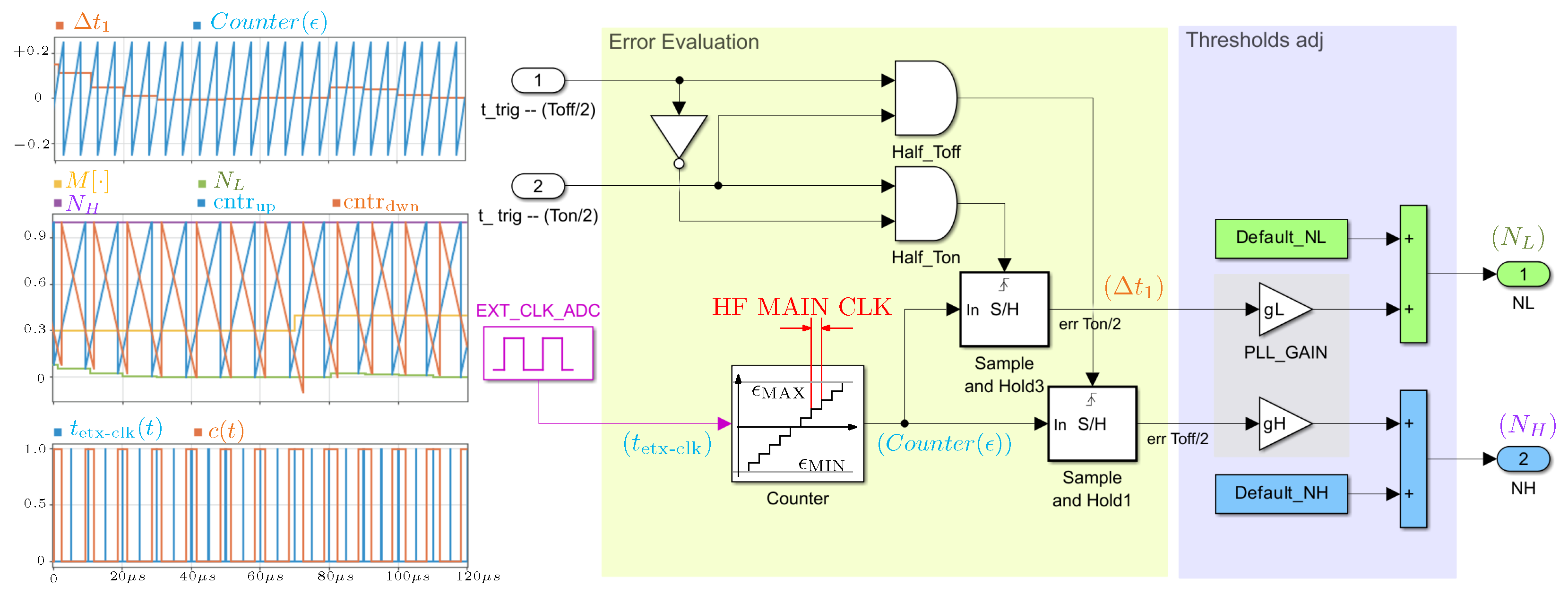
3.2. Synchronization Mechanism

As mentioned before, another critical aspect of ADE-DPWM architectures lies in the lack of an intrinsic synchronization mechanism. Differently, as discussed in the previous section, the proposed enhanced DPWM structure offers a considerable advantage in this regard, since it intrinsically guarantees the generation of a signal (i.e., the one generated in correspondence of the intersection between the two carriers highlighted with the red dots in Figure 4 and Figure 6) that can be used to trigger the sampling actions on piecewise linear inductor currents. To understand the issue, refer to a Buck-type DC–DC converter (this topology is chosen as a remarkable example given its widespread use in various power electronics applications. In addition, the issue of average current sampling is in common with several topologies derived from the Buck; one among them is the voltage source inverter). The schematic of the Buck converter with the digital control scheme and the eDPWM is shown in Figure 7. The average current is generally calculated from a single sample acquired exactly halfway through the ON phase or OFF phases or at both points for controls that use double-sampling of state variables and double-updating of control signals. With the proposed eDPWM architecture, one can use the intersection between the two carriers to acquire the current at the midpoint. This ensures that the average inductor current I L 1 T s t o T s + t o i L ( t ) d t is acquired correctly on each ON and/or OFF phase.
One can define the signal t trig that is set to 1 when the intersection of the two carriers occurs during the ON phase. When the intersection occurs during the OFF phase, the signal is reset to zero. This signal can be used to trigger the A D C 1 in Figure 7. This sampling system, at a fixed frequency when the converter is operating in steady-state and at variable frequency during transients, is already able to obtain the correct average value of the i L ( t ) current.
Implementing the average inductor current acquisition reported in Figure 7 with the ADE-DPWM proposed in [23] requires the additional digital hardware reported in the structure of Figure 8. Indeed, the ADE-DPWM architecture does not intrinsically offer the trigger instant at the middle of ON and OFF phases. Cycle-per-cycle, phase-per-phase, one must compute this instant starting from the acquired value of the modulating signal. This calculation can be done in FPGA at the price of an increased complexity. The proposed eDPWM having naturally this trigger instant, does not need the structure in Figure 8; this drastically reduces the overall system complexity.
Some system prerequisites may require synchronization with an external clock ( t ext-clk ( t ) ). In this case, t trig can be used to measure the synchronism error with respect to t ext-clk ( t ) .
This error can be therefore corrected in a few switching cycles. This mechanism acts as a phase-locked loop (PLL). This operation is indicated as ext-synch-mode. Figure 9 reports the corresponding MATLAB/Simulink implementation and the simulation results for the eDPWM v2.0 operating in ext-synch-mode.
The ADC is clocked with the external fixed-frequency clock t ext-clk ( t ) ; this is represented with the blue narrow signal at the bottom-left of Figure 9. The counter is triggered by the rising edge of t etx-clk ( t ) and starts to count. The value of the counter is sampled when the signal t trig rises. This value represents the distance between the sampling point and the half of the ON phase. This error is therefore used to correct the upper and lower thresholds, N L and N H (for simplicity in the simulation reported in Figure 9, only the lower threshold is moved since g H = 0 ).
The simulation in Figure 9 starts intentionally from the wrong initial conditions. Due to this, one has an initial synchronization error. This is the distance between the sampling instant and the middle of the ON phase. In the proposed simulation, ≈90% of the initial error is recovered in two modulation cycles. Furthermore, a modulating signal step is performed after 70 μs. The system still managed to resynchronize in only two cycles (≈90% of the error). Note that the action of the synchronization error correction could be performed in a deadbeat fashion. However, this could lead to instability and oscillation problems in closed-loop systems. Therefore, the proposed PLL-like mechanism is deliberately slowed down.
The same mechanism can also be implemented in the ADE-DPWM. However, it would be necessary to process cycle-by-cycle, phase-ON and phase-OFF where they are the midpoints of each phase, and then estimate the error with respect to the external clock. Figure 8 shows the synchronization systems of the double-sampling ADE-DPWM proposed in [23]. Here, the threshold modulation can only be done according to the synchronization error detected during the ON phase. To detect (and correct) the synchronization error with respect to the external clock, even during the OFF phase, the blocks highlighted with the red arrow must be replicated. The synchronization system in the proposed eDPWM v2.0 architecture does not have this constraint, and the structure in Figure 9 is capable of correcting the error on both thresholds according to the sampling error position acquired during both the ON and OFF phases. The blocks used in Figure 8 and Figure 9 represent the MATLAB/Simulink implementation. These can be directly implemented in VHDL or Verilog codes.
Finally, both the proposed eDPWM and the ADE-DPWM in [23] can be used to generate the trigger instant for the ADC in both ext-synch-mode and internal synch-mode. The main difference is that in the eDPWM the computation block in Figure 8 is not required since it intrinsically provides the synchronization instant at the middle of the ON and OFF phases. Furthermore, moving the N H and N L thresholds in an ADE-DPWM architecture in order to synchronize with an external signal (i.e., when the synchronization mechanism is used as a PLL) is complex since the thresholds are scaled according to the counting step required to achieve fractional slopes.
Compared with the architectures proposed in [23,24,25,26], the additional hardware required to operate in ext-synch-mode is more contained in the proposed architecture. In fact, since there is no need to estimate, cycle by cycle, the point corresponding to the middle of the ON or OFF phase, the mechanism to operate with an external trigger is reduced to an additional counter and two sum operations to update the threshold values.
The next section derives the expressions of the time domain operation, showing that these are the same as those obtained in [23]. The small signal model is therefore discussed and commented.

4. The Small Signal Model

This section proves the time domain equivalence between the ADE-DPWM in [23] and the eDPWM V2.0. Once proved their equivalence in steady-state and during transients, the small signal model is uniquely identified. It is then necessary to prove their equivalence in the time domain only.

4.1. Time Domain Operation

Figure 6 and Figure 10 are used as a reference in the following analysis.
The variation of the ON and OFF phases for the i-th cycle, named as Δ x on [ i ] and Δ x off [ i ] , can be calculated as
Δ x on [ i ] = Δ x n 1 + Δ x n 2 ; Δ x off [ i ] = Δ x f 1 Δ x f 2
where the quantities Δ x n 1 , Δ x n 2 , Δ x f 1 and Δ x f 2 are defined in Figure 10.
Let’s start with Δ x off [ i ] . By analyzing Figure 6 and Figure 10 one has
Δ x f 1 = Δ M on [ i ] ; Δ x f 2 = b Δ m off [ i ] .
By using (8) and by substituting the definitions of Δ M on [ i ] and Δ m off [ i ] M off [ i ] M on [ i ] in (7) one obtains
Δ x off [ i ] = Δ x f 1 + Δ x f 2 = b ( M off [ i ] M on [ i ] ) + M on [ i ] M ss = b ( M off [ i ] M ) + b M ss M on [ i ] ( 1 b ) M ss = b Δ M off [ i ] Δ M on [ i ] ( 1 b ) .
With identical approach, by using Figure 6 and Figure 10 as a reference, one has
Δ x n 1 = Δ M off [ i 1 ] ; Δ x n 2 = a Δ m on [ i ] .
By substituting the definitions of Δ M off [ i 1 ] and Δ m on [ i ] M on [ i ] M off [ i 1 ] in (10) one obtains
Δ x on [ i ] = Δ x n 1 + Δ x n 2 = a Δ M on [ i ] Δ M off [ i 1 ] ( 1 a ) .
Using (9) and (11), one can calculate the net variation of the switching period x s [ i ] as
Δ x s [ i ] x s [ i ] x s = Δ x on [ i ] + Δ x off [ i ] = Δ M on [ i ] ( a + 1 b ) Δ M off [ i ] b Δ M off [ i 1 ] ( 1 a ) .
Equations (9), (11), and (12) describe the time domain operation of the proposed eDPWM V2.0. Those equations are exactly the same as those in [23].

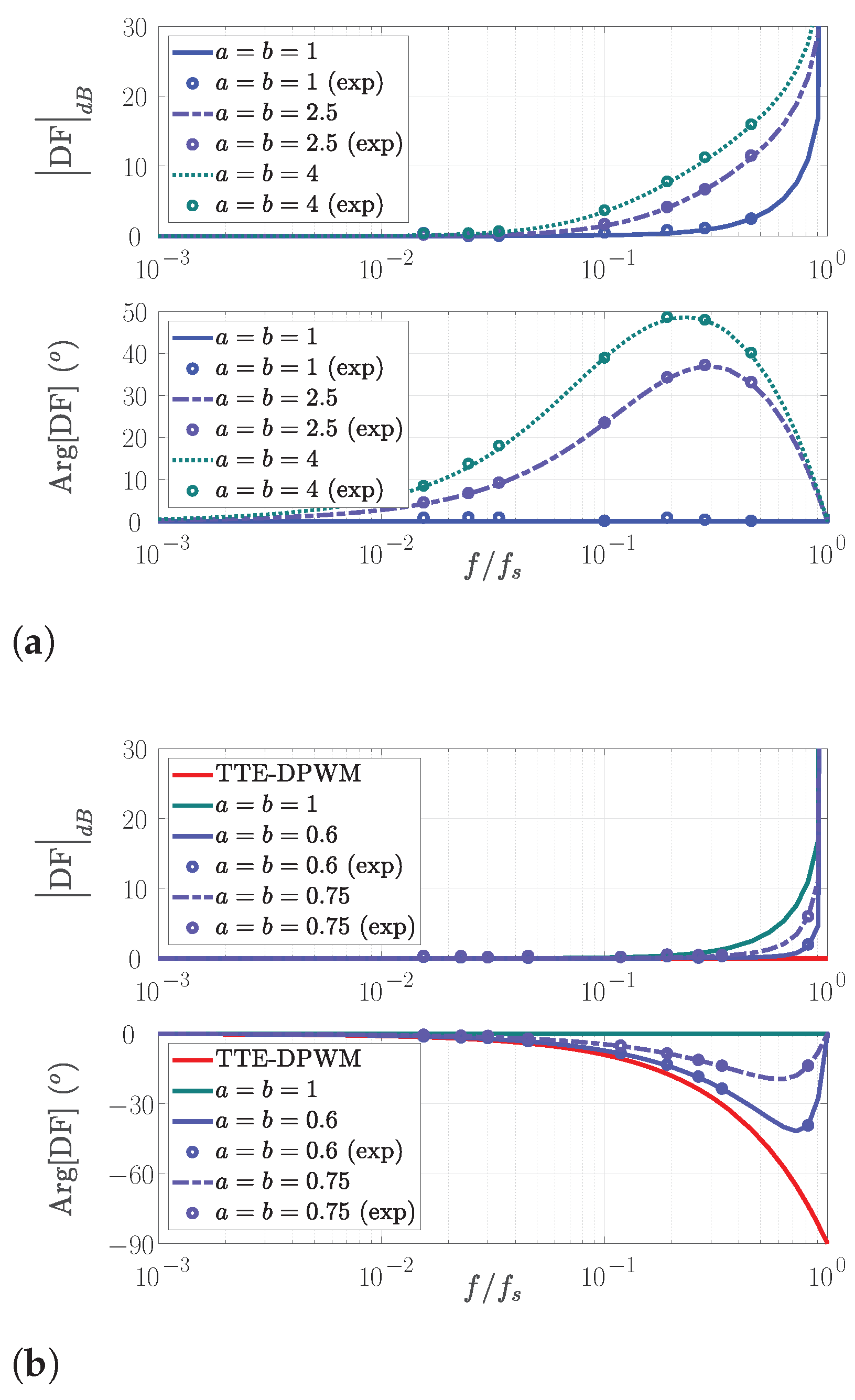
4.2. Frequency Domain Results

Since, as proven in the previous section, the time domain model of the proposed architecture is identical to that of the ADE-DPWM architecture in [23], the small signal model in the frequency domain will be the same. In fact, as for the Fourier Transformation, a describing function is completely identified by its time domain expression. In other words, an equivalent representation in the time domain implies an identical describing function model. Thus, the small signal model of eDPWM V2.0 coincides with the small signal model of the double-sampling ADE-DPWM developed in [23]. The model in [23] is obtained by using the describing function approach. Given the redundancy, the frequency domain analysis is not reported in this manuscript. For the mathematical derivation, one can refer to [23]. For completeness, only the procedure in broad outline is given below.
For the small signal analysis, a small-sinusoidal perturbation u ^ ( t ) is superimposed on a constant modulating signal value M ss
u ^ ( t ) = a ^ sin 2 π f k T s x ϕ with a ^ M ss .
The Fourier analysis is therefore conducted on the output signal c ( t ) (i.e., C F = F { c ( t ) } ) (the symbol F denotes the Fourier Transform Operator). In steady-state with u ^ ( t ) = 0 , c ( t ) is a signal with a main frequency component at f s . When the perturbation u ^ ( t ) as in (13) with a main frequency component at f k is superimposed at the constant input M ss , the output control signal c ( t ) becomes a signal with a main frequency component around f res , which is the inverse of the minimum common multiple from T s = 1 / f s and T k = 1 / f k , i.e.,
T res = 1 / f res = N T k + K T s with N , K N prime integers .
The small signal model is finally obtained by computing the ratio between the Fourier coefficient C F evaluated at f res and the Fourier coefficient of u ^ ( t ) computed at f k .
The final result coincides with that in [23] (or more generally in [24]). The final expression in the frequency domain is given below. This is identical to that in [23] by substituting a = α and b = β . The terms have been arranged to better emphasize the different contributions. Thus, the small signal model of the proposed eDPWM is
G eDPWM 2 ( s ) = e s T s 2 x on 1 e s T s 1 e s T s a + ( 1 a ) e s T s 2 + e s T s x on 1 e s T s x on 1 e s T s ( a 1 ) 1 e s T s 2 + b ( 1 e s T s 2 ) ,
where s C is the complex variable of the Laplace plane. In the practical cases with a = b , one has
G eDPWM 2 ( s ) = e s T s 2 x on 1 e s T s a 2 e s T s 2 1 e s T s e s T s 2 + 1 + e s T s x on 2 1 e s T s 2 a a e s T s 2 + e s T s 2 + e s T s 2 1 .
In the simplified case for a = b = 1 , one has
G eDPWM 2 ( s ) | a = b = 1 = e s T s 2 x on 1 e s T s x on 1 e s T s 1 e s T s 2 .
The proposed eDPWM V2.0 architecture, reported in Figure 5a, keeps the same small signal behavior of the complex architecture in [23]. In this section, the equivalence between the two architectures is proved through the time domain analysis. This analysis revealed that the behavior of the proposed eDPWM V2.0 solution is identical to that of the architecture in [23]. Unlike the latter, however, the proposed solution does not need the computation of products between signals and no division by generic parameters. In addition, the counters are completely standard and do not have to change the counting step, avoiding perishing to degrade the resolution with which the counting ramp variables are represented.
The final eDPWM V2.0 architecture is available as MATLAB/Simulink block diagram in the open-source resource (CC BY 4.0) (Supplementary Materials).

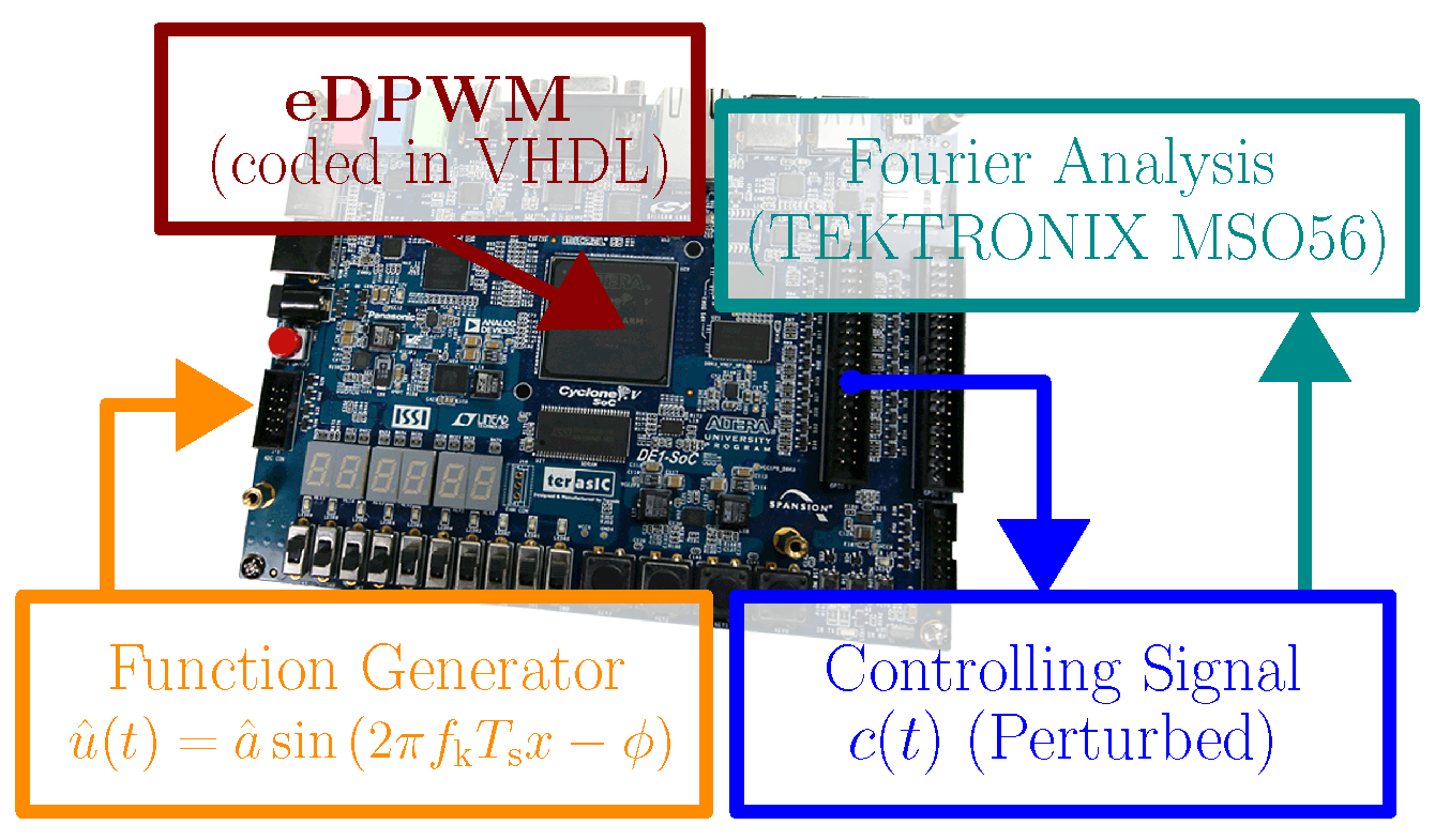
5. Experimental Validation

To further validate the proposed simplified double-sampling eDPWM V2.0 architecture reported in Figure 5a, a set of experimental measurements is reported below. The proposed modulator’s architecture is coded in VHDL and implemented in a commercial Intel© Cyclone©Ṽ 5CSEMA5F31C6N FPGA. This FPGA is contained in the TerasIC© De1-SoC Development Board. Board was purchased on Mouser Electronics©.
The experimental setup organization is reported in Figure 11. The external sinusoidal perturbation is sampled with the onboard 12-bit LTC 2308 ADC ( f sample = 500   kHz ). The ADC output data are serial. This increases the overall latency ( t ADC-latency ) since one must wait for the full word acquisition before sending it to the eDPWMṪhe ADC latency and its consequent phase rotation (i.e., ≈ e t ADC-latency s ) must be therefore taken into account and compensated in the final experimental data. Given the limited capabilities of the ADC, the steady-state modulating period is fixed at f s = 20   kHz . The perturbation frequency range (values of f k ) is 200   Hz ÷ 15   kHz . The Fourier analysis is performed with the Tektronix M S 056 .
The experimental results are compared with the theoretical curves in Figure 12. Figure 12a shows analytical curves and experimental data for different values of a = b . The curve obtained for a = b = 4 shows a peak phase boost of ϕ boost 50 for f f s / 4 . Such phase boost gain can be exploited in closed-loop systems (e.g., Figure 7) to enhance the dynamic performance. Generally, a system’s bandwidth is a compromise between speed and stability margins. Particularly critical is the phase margin parameter. By having a phase boost right around the crossing frequency, it is therefore possible to increase the bandwidth without degrading the phase margin. Similar considerations and experimental tests are proposed in [23,24,25,29,30].
Figure 12a shows the analytical curves and experimental data for a = b < 1 . The figure also shows the response of a TTE-DPWM [28] as a reference to show how even small values of a = b < 1 can lead to large improvements in terms of available phase compared with what is the most commonly used solution.

Discussion

The comparison between experimental and theoretical curves shows three important facts. The first is that the analytical model is correct and able to predict the behavior of the modulator over the entire frequency range of interest (i.e., f < f NYQUIST ). Since the frequency model is derived from the time domain model, the comparison indirectly proves that the time domain model is also correct. The second remarkable element is that, despite the radical simplification of the architecture, the proposed eDPWM can achieve the same results as the double-sampling ADE-DWPM architecture. The third interesting fact can be noticed when a = b < 1 . Comparing the results obtained by the proposed architecture with the more conventional TTE-DPWM, it can be seen that even with a = b < 1 , a significant increase in the high-frequency phase, up to ϕ boost 90 , can be obtained. This fact is significant because while small values of a = b allow for the containment of possible high-frequency noise due to the presence of a derivative action, on the high side it still allows a designer to achieve a required phase gain when compared with conventional DPWM architectures. This fact is not further investigated in this article for reasons of space.
Another key aspect is the direct comparison with the architecture in [23]. The implementation of the ADE-DPWM architecture in [23] requires a large amount of resources. A fully functional implementation with programmable parameters a and b can be set up as follows. The system clock is set at f clk-ADE = 400   MHz (e.g., by using a PLL and starting from the system’s fundamental clock which is f sys-clk = 50   MHz ).
With this, the maximum resolution of the DPWM is q MAX = 20   kHz / 400   MHz = 1/20,000. The ADE-DPWM architecture uses fractional counts to set the slopes’ values (i.e., S / a and S / b ). To obtain such divisions, the resolution of the modulator must be reduced up to q ADE = 1 / 1000 . Thus, there are 20 cycles at 400   MHz between two consecutive count increments. With this organization, the variable slopes of the ADE-DPWM counters in [23] can be achieved. The true implementation of the slope divisions uses different count steps and normalization factors depending on the slope to be set. This can be handled by selection structures (e.g., IF/THEN type).
The eDPWM architecture requires fewer resources than the ADE-DPWM. Indeed, the system clock can be set to f clk-eDPWM = 20   MHz , and the eDPWM resolution is q eDPWM = 20   kHz / 20   MHz = 1 / 1000 . The 20 clock cycles between two consecutive increments of the counters are not required anymore since in the eDPWM architecture the counters do not use fractional slopes. Therefore, the final system resolution is the same as the ADE-DPWM but now a system clock that is 20 times slower is adopted. Also, selection structures like IF/THEN are not required to set count steps and scaling factors.
There are several other simplifications in the eDPWM architecture, but this one is the most remarkable. The experimental tests show consistency with the analytical model developed, even after relaxing the system specification as described above. Since the analytical model of eDPWM is the same as that in [23], these tests can also be used to prove experimental equivalence with the ADE-DPWM, even with more relaxed system specifications.

6. Conclusions

This work proposes and analyzes an innovative Digital Pulse Width Modulator architecture that eliminates the typical delays associated with conventional designs. The enhanced DPWM introduces a variable frequency modulation strategy with a programmable derivative action, enabling a significant improvement in the dynamic response of digital control systems. Theoretical analysis and experimental tests have demonstrated the equivalence of the eDPWM with advanced solutions from the literature, while drastically reducing computational complexity. Additionally, the proposed structure incorporates an intrinsic synchronization mechanism that facilitates the acquisition of the average inductor current, simplifying its implementation in power electronics applications.
Experimental tests conducted on an FPGA implementation have validated the effectiveness of the proposed architecture, highlighting improved high-frequency phase performance and greater flexibility compared to traditional DPWM techniques. By reducing complex operations and eliminating the need for multiplications and divisions between signals, the eDPWM emerges as an efficient and easily implementable solution for both industrial and academic applications. Future research may explore further optimizations relating to its integration with other advanced control techniques for power electronics.

Supplementary Materials

The following supporting information can be downloaded at: https://www.mdpi.com/article/10.3390/electronics14081522/s1.

Funding

This research received no external funding.

Data Availability Statement

The open-source (CC BY 4.0) MATLAB code and the Simulink implementation of the final eDPWM V2.0 architecture is available on Supplementary Materials.

Acknowledgments

This study was carried out within the MOST—Sustainable Mobility Center and received funding from the European Union Next-GenerationEU (PIANO NAZIONALE DI RIPRESA E RESILIENZA (PNRR)—MISSIONE 4 COMPONENTE 2, INVESTIMENTO 1.4—D.D. 1033 17 June 2022, CN00000023). This manuscript reflects only the authors’ views and opinions; neither the European Union nor the European Commission can be considered responsible for them.

Conflicts of Interest

The author declares no conflicts of interest.

Abbreviations and Main Definitions

The following abbreviations are used in this manuscript:
SymbolDefinition
DPWMDigital Pulse Width Modulator;
eDPWMEnhanced Digital Pulse Width Modulator;
ADEAsymmetric Dual-Edge;
TTETrailing-Triangle Edge;
T s Modulation period;
T on ON time of the pulse width modulation cycle;
T off OFF time of the pulse width modulation cycle;
x on Normalized ON phase duration (i.e., T on T s );
x off Normalized OFF phase duration (i.e., T off T s );
x on [ i ] Normalized ON phase duration during the i-th cycle;
x off [ i ] Normalized OFF phase duration during the i-th cycle;
Δ x on [ i ] Variation of the ON phase during the i-th cycle (i.e., x on [ i ] x on );
Δ x off [ i ] Variation of the OFF phase during the i-th cycle (i.e., x off [ i ] x off );
M [ · ] Modulating signal;
M ss Steady-state value of the modulating signal;
Δ M on Modulating signal variation during the ON phase;
Δ M off Modulating signal variation during the OFF phase;
SCarrier slope;
sComplex independent variable of the transfer functions;
c ( t ) Output control signal;
G eDPWM ( s ) Small signal transfer function of the eDPWM V2.0;
f s Steady-state switching frequency;
f k Frequency of the input perturbation;
ϕ boost High-frequency phase boost;
PLLPhase-Locked Loop;
a , b Parameters to weight the derivative action;
N H , N L Upper and lower DPWM thresholds.

References

  1. Li, W.; He, X. Review of Nonisolated High-Step-Up DC/DC Converters in Photovoltaic Grid-Connected Applications. IEEE Trans. Ind. Electron. 2011, 58, 1239–1250. [Google Scholar] [CrossRef]
  2. Forouzesh, M.; Siwakoti, Y.P.; Gorji, S.A.; Blaabjerg, F.; Lehman, B. Step-Up DC–DC Converters: A Comprehensive Review of Voltage-Boosting Techniques, Topologies, and Applications. IEEE Trans. Power Electron. 2017, 32, 9143–9178. [Google Scholar] [CrossRef]
  3. Mao, H.; Lee, C.; Boroyevich, D.; Hiti, S. Review of high-performance three-phase power-factor correction circuits. IEEE Trans. Ind. Electron. 1997, 44, 437–446. [Google Scholar] [CrossRef]
  4. de Castro, A.; Todorovich, E. High Resolution FPGA DPWM Based on Variable Clock Phase Shifting. IEEE Trans. Power Electron. 2010, 25, 1115–1119. [Google Scholar] [CrossRef]
  5. Le, H.; Dekka, A.; Ronanki, D.; Rodriguez, J. Predictive Current Control of a New Four-Level Voltage Source Inverter. In Proceedings of the 2022 IEEE International Conference on Power Electronics, Drives and Energy Systems (PEDES), Jaipur, India, 14–17 December 2022; pp. 1–5. [Google Scholar] [CrossRef]
  6. Buso, S.; Mattavelli, P. Digital Control in Power Electronics, 2nd ed.; Springer: Cham, Switzerland, 2015. [Google Scholar]
  7. Sozański, K. Digital Signal Processing in Power Electronics Control Circuits, 2nd ed.; Springer: Cham, Switzerland, 2013. [Google Scholar]
  8. Buccella, C.; Cecati, C.; Latafat, H. Digital Control of Power Converters—A Survey. IEEE Trans. Ind. Inf. 2012, 8, 437–447. [Google Scholar] [CrossRef]
  9. Kelly, A.; Rinne, K. High Resolution DPWM in a DC-DC Converter Application Using Digital Sigma-Delta Techniques. In Proceedings of the 2005 IEEE 36th Power Electronics Specialists Conference, Recife, Brazil, 12–16 June 2005; pp. 1458–1463. [Google Scholar] [CrossRef]
  10. Huang, Y.; Cheung, C. Small signal modeling of the hysteretic modulator with a current ripple synthesizer. In Proceedings of the 2016 IEEE Applied Power Electronics Conference and Exposition (APEC), Long Beach, CA, USA, 20–24 March 2016; pp. 1616–1623. [Google Scholar] [CrossRef]
  11. Rodriguez, J.; Pontt, J.; Silva, C.A.; Correa, P.; Lezana, P.; Cortes, P.; Ammann, U. Predictive Current Control of a Voltage Source Inverter. IEEE Trans. Ind. Electron. 2007, 54, 495–503. [Google Scholar] [CrossRef]
  12. Singh, R.K.; Mishra, S. Synthetic-Ripple-Based Digital Hysteretic Modulator for Point-of-Load Converters. IEEE Trans. Ind. Electron. 2013, 60, 4996–5007. [Google Scholar] [CrossRef]
  13. Malesani, L.; Tenti, P. A novel hysteresis control method for current-controlled voltage-source PWM inverters with constant modulation frequency. IEEE Trans. Ind. Appl. 1990, 26, 88–92. [Google Scholar] [CrossRef]
  14. Nussbaumer, T.; Heldwein, M.L.; Gong, G.; Round, S.D.; Kolar, J.W. Comparison of Prediction Techniques to Compensate Time Delays Caused by Digital Control of a Three-Phase Buck-Type PWM Rectifier System. IEEE Trans. Ind. Electron. 2008, 55, 791–799. [Google Scholar] [CrossRef]
  15. Corradini, L.; Mattavelli, P.; Tedeschi, E.; Trevisan, D. High-Bandwidth Multisampled Digitally Controlled DC–DC Converters Using Ripple Compensation. IEEE Trans. Ind. Electron. 2008, 55, 1501–1508. [Google Scholar] [CrossRef]
  16. Petric, I.Z.; Mattavelli, P.; Buso, S. A Jitter Amplification Phenomenon in Multisampled Digital Control of Power Converters. IEEE Trans. Power Electron. 2021, 36, 8685–8695. [Google Scholar] [CrossRef]
  17. Corradini, L.; Mattavelli, P.; Saggini, S. Elimination of Sampling-Induced Dead Bands in Multiple-Sampled Pulsewidth Modulators for DC–DC Converters. IEEE Trans. Power Electron. 2009, 24, 2661–2665. [Google Scholar] [CrossRef]
  18. Petric, I.Z.; Mattavelli, P.; Buso, S. Investigation of Nonlinearities Introduced by Multi-sampled Pulsewidth Modulators. IEEE Trans. Power Electron. 2022, 37, 2538–2550. [Google Scholar] [CrossRef]
  19. Chen, J.; Prodic, A.; Erickson, R.; Maksimovic, D. Predictive digital current programmed control. IEEE Trans. Power Electron. 2003, 18, 411–419. [Google Scholar] [CrossRef]
  20. Mohamed, Y.A.R.I.; El-Saadany, E.F. Robust High Bandwidth Discrete-Time Predictive Current Control with Predictive Internal Model—A Unified Approach for Voltage-Source PWM Converters. IEEE Trans. Power Electron. 2008, 23, 126–136. [Google Scholar] [CrossRef]
  21. Mattavelli, P. An improved deadbeat control for UPS using disturbance observers. IEEE Trans. Ind. Electron. 2005, 52, 206–212. [Google Scholar] [CrossRef]
  22. Bonanno, G.; Corradini, L. Digital Predictive Current-Mode Control of Three-Level Flying Capacitor Buck Converters. IEEE Trans. Power Electron. 2021, 36, 4697–4710. [Google Scholar] [CrossRef]
  23. Bonanno, G.; Comacchio, A.; Mattavelli, P.; Corradin, M. Asymmetric Dual-Edge Digital Pulsewidth Modulator With an Intrinsic Derivative Action. IEEE Trans. Power Electron. 2023, 38, 304–315. [Google Scholar] [CrossRef]
  24. Bonanno, G.; Comacchio, A.; Mattavelli, P. Multisampling Digital Pulse-Width Modulator Based on Asymmetric Dual-Edge Carrier. IEEE Trans. Power Electron. 2024, 39, 5121–5134. [Google Scholar] [CrossRef]
  25. Comacchio, A.; Bonanno, G.; Hossein, A.; Mattavelli, P.; Corradin, M. A Digital Dual-Edge Modulator for Dynamic Performance Improvement of Multi-Loop Controlled VSI. IEEE Trans. Ind. Electron. 2022, 70, 4662–4671. [Google Scholar] [CrossRef]
  26. Cvetanovic, R.; Bonanno, G.; Comacchio, A.; Abedini, H.; Biadene, D.; Mattavelli, P. High Frequency Passivity Properties of Grid-Connected Admittance With Double-Sampling Asymmetric Dual-Edge Modulator. IEEE Open J. Power Electron. 2022, 3, 856–865. [Google Scholar] [CrossRef]
  27. da Silva Carvalho, S.; Halamíček, M.; Vukadinović, N.; Prodić, A. Digital PWM for Multi-Level Flying Capacitor Converters with Improved Output Resolution and Flying Capacitor Voltage Controller Stability. In Proceedings of the 2018 IEEE 19th Workshop on Control and Modeling for Power Electronics (COMPEL), Padova, Italy, 25–28 June 2018; pp. 1–7. [Google Scholar] [CrossRef]
  28. Corradini, L.; Maksimović, D.; Mattavelli, P.; Zane, R. Digital Control of High-Frequency Switched-Mode Power Converters; Wiley: Hoboken, NJ, USA, 2015; pp. 1–342. [Google Scholar] [CrossRef]
  29. Ripamonti, G.; Saggini, S.; Corradini, L.; Rizzolatti, R.; Faccio, F.; Michelis, S.; Koukab, A.; Kayal, M. A Dual-Edge Pulsewidth Modulator for Fast Dynamic Response DC-DC Converters. IEEE Trans. Power Electron. 2019, 34, 28–32. [Google Scholar] [CrossRef]
  30. Huang, Y.; Cheung, C.; Jayaprakash, K.V.A. Small signal modeling of dual-edge PWM modulator with fixed clock frequency. In Proceedings of the 2017 IEEE Applied Power Electronics Conference and Exposition (APEC), Tampa, FL, USA, 26–30 March 2017; pp. 1047–1053. [Google Scholar] [CrossRef]
Figure 1. Exemplified time operation of (blue lines) TTE-DPWM and (black lines) double-sampling ADE-DPWM and corresponding control signals. Gray lines represent the steady-state operation while the double-sampled modulating signal is represented in magenta.
Electronics 14 01522 g001
Figure 2. Comparison between double-sampling ADE-DPWM (top) and the proposed eDPWM v1.0 (bottom). Blue and green lines are respectively used to highlights the counters used for computing the ON and OFF phases duration.
Electronics 14 01522 g002
Figure 3. Details of the operation of eDPWM v1.0. Color scheme is kept consistent with previous representations.
Electronics 14 01522 g003
Figure 4. Operation of the double-sampling ADE-DPWM (top) vs. eDPWM V1.5 (bottom). Red dots represent the carrier intersections.
Electronics 14 01522 g004
Figure 5. MATLAB/Simulink block implementation of the double-sampling (a) eDPWM v2.0 and (b) ADE-DPWM proposed in [23]. Region in turquoise highlights the blocks required to perform the derivative action. The MATLAB version is the 2024a.
Electronics 14 01522 g005
Figure 6. Operation of the DS ADE-DPWM with an intrinsic derivative action from [23] (top) vs. the eDPWM v2.0 (bottom). Green and blue lines are used to respectively highlights the counter used for computing the ON and OFF phases. Red dots indicates the intersection between the two carries in the eDPWM v2.0.
Electronics 14 01522 g006
Figure 7. Standardapplication of a multi-loop digital control scheme for a Buck converter using the eDPWM modulator to acquire the average inductor current with a synchronous or asynchronous sampling mechanism. Colored lines denotes the dynamic operation while gray lines represent the steady-state operation.
Electronics 14 01522 g007
Figure 8. MATLAB/Simulink implementation of the synchronism mechanism of the double-sampling ADE-DPWM proposed in [23].
Electronics 14 01522 g008
Figure 9. MATLAB/Simulink simulation results of the eDPWM v2.0 (with a = b = 1 ) running in ext-synch-mode with an external reference clock. On the right side is the Simulink implementation of the synchronization mechanism; on the left side are the simulation results. HF MAIN CLK indicates the high-frequency main system clock.
Electronics 14 01522 g009
Figure 10. Details of the operation of the proposed derivative ADE-DPWM during (a) the off-phase and (b) the off-phase. Gray lines represent the steady-state while black lines represent the operation during transients.
Electronics 14 01522 g010
Figure 11. Organization of the experimental setup.
Electronics 14 01522 g011
Figure 12. (a) Bode plots of G eDPWM 2 ( s ) for different values of a = b and M ss = 0.5 : gain (on top) and angle (on bottom). (b) Bode plots of G eDPWM 2 ( s ) for different values of a = b vs. the traditional double-sampling Trailing-Triangle edge carrier-based DPWM (TTE-DPWM). The experimental data are highlighted with dots. The x-axes are normalized with respect to the steady-state switching frequency f s .
Electronics 14 01522 g012
Table 1. Comparison of double sampling DPWM architectures. () A positive phase-boost can be programmed. () May be implemented in some MCUs.
ArchitecturePhase DelayComput. ComplexityHardware Suitability
TTE e s T s / 4 LowSimple for MCUs and FPGAs
ADEzero HighOnly FPGA
eDPWMzero LowEfficient on FPGA
Disclaimer/Publisher’s Note: The statements, opinions and data contained in all publications are solely those of the individual author(s) and contributor(s) and not of MDPI and/or the editor(s). MDPI and/or the editor(s) disclaim responsibility for any injury to people or property resulting from any ideas, methods, instructions or products referred to in the content.

