Abstract
This study proposes an optimal resonant network design for an 11.1 kW wireless power transfer (WPT) system with a double-sided LCC compensation circuit, targeting 800 V class battery applications. Conventional WPT circuit topologies and design parameters specified in existing standards, such as SAE J2954, are unsuitable for 800 V class battery systems because they impose excessive voltage and current stresses on the resonant network components. To address this, the proposed design focuses on minimizing component stresses while ensuring compliance with the output voltage requirements for 800 V battery charging. A switched capacitor technique is integrated into the resonant network to dynamically adjust the compensation capacitance, enabling seamless adaptation to the constant current–constant voltage charging profile. The feasibility of the WPT system is validated through simulations and experiments, demonstrating an input voltage of 400 VDC, an output voltage range of 560–820 VDC, and a rated power capacity of 11.1 kW. Under rated conditions, the system achieves a peak efficiency of 95%, underscoring its practicality for high-voltage electric vehicle charging applications.
1. Introduction
Wireless power transfer (WPT) systems utilizing inductive coupling have been widely implemented in diverse applications, from portable devices to industrial settings, owing to their high flexibility and convenience in delivering power at elevated power levels and efficiencies. Recent advancements in WPT technology have encompassed research spanning small-scale electronics, such as smartphones and medical devices, to high-power applications, such as electric vehicles (EVs) [1,2,3].
Among these, WPT systems for EV charging typically adhere to the SAE J2954 wireless charging standard established by the Society of Automotive Engineers (SAE). This standard defines the permissible criteria for interoperability, electromagnetic compatibility, electromagnetic field limits, minimum performance, safety, and testing protocols for EV wireless charging, thereby regulating specifications across industries. EV wireless charging systems are categorized into WPT 1, 2, and 3 classes based on their rated power, with the WPT 3 Class targeting 11.1 kW. Although SAE J2954 provides critical guidelines for circuit topologies, mechanical configurations, and electrical test stations, these specifications are tailored for 400 V class battery systems [4].
However, recent advancements in automotive power electronics, along with the rapidly increasing demand for high-speed charging, have accelerated the transition toward 800 V architectures. Compared with conventional 400 V systems, 800 V systems offer several technical advantages, including reduced conduction losses, improved efficiency in the power conversion stages, and significantly faster charging speeds enabled by lower current requirements. These benefits enhance the overall performance of electric vehicles and facilitate the integration of advanced high-power components into the powertrain, resulting in more compact and lightweight electrical systems [5]. Furthermore, the growing need for an extended driving range and reduced charging times has driven a strong industry trend toward high-voltage system designs, making 800 V platforms increasingly attractive for next-generation electric vehicles [6].
Research on WPT systems for EV wireless charging that support 800 V class batteries is being actively conducted. In addition, various studies have been conducted to enhance the performance of EV wireless charging WPT systems. In [7], a WPT system was proposed that could charge electric vehicles equipped with either a 400 or 800 V nominal battery voltage at the same power level of 7.2 kW. This was achieved by employing two sets of series-compensated coupled coils, referred to as voltage/current doublers. Similarly, ref. [8] proposed a novel single-stage reconfigurable inductive charger capable of charging both 400 and 800 V battery packs at a rated power of 3.3 kW using a single coupler and minimal conversion stages. In [9], an advanced WPT system featuring active load impedance matching in the rectification stage was introduced, along with a practical implementation for 800 V class EV charging and the corresponding experimental results.
Other recent studies include the introduction of decoupling coils with variable self-inductance to accommodate variations in the coil separation distance [10]; investigations into core materials and arrangements to improve the performance of charging pads [11,12,13]; analysis of coil shape, interoperability, and misalignment effects [14,15,16]; and studies on foreign object detection (FOD) in EV wireless charging systems [17,18]. Despite these diverse contributions, detailed analyses of the resonant compensation network, which is essential to WPT systems, and the voltage and current stresses imposed on network components have not been extensively explored.
Given the nature of inductively coupled WPT systems, the resonant network is one of the most critical components in the system design. In WPT systems for EV charging, the vertical separation between the transmitter and receiver coils, dictated by the ground clearance of the vehicle, results in a significantly low coupling coefficient, which quantifies the magnetic coupling level between the coils. Typically, the coupling coefficient varies between 5% and 30%, depending on the distance, alignment, and dimensions of the coils. In WPT systems, energy is transferred through the mutual inductance of the coils, whereas the leakage inductance does not contribute to active power transfer [19].
Therefore, in inductively coupled WPT systems, power transfer using only the transmitter and receiver coils leads to an increased volt-ampere rating on the transmitter side and limited power delivery capacity on the receiver side. To address this issue, resonant circuits are typically implemented by integrating capacitors that cancel the leakage inductance to form a compensation circuit. As mentioned previously, the primary role of compensation circuits in WPT systems is to eliminate the reactive power caused by leakage inductance. The inductors and capacitors in these circuits can be combined in numerous configurations if they satisfy the resonant frequency condition. However, the selection of inductor and capacitor values in the compensation circuit directly affects the voltage/current stresses imposed on the components and the overall physical size of the system [20].
Accordingly, this study adopts a double-sided LCC (DS-LCC) compensation topology, which is currently utilized in the SAE J2954 standard despite various types of compensation circuits having been proposed and implemented in the literature [21,22,23]. In this topology, both the transmitter and receiver sides consist of one inductor and two capacitors. The WPT system employing the DS-LCC compensation network was configured as shown in Figure 1, and the same circuit topology was used without any modifications to the system configuration, simulation, or experimental validation.
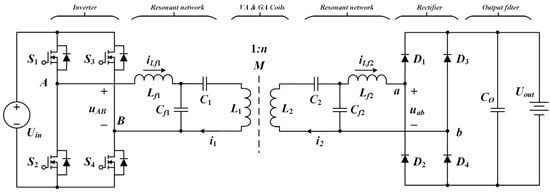
Figure 1.
WPT system with double-sided LCC compensation circuit.
Based on the above, this paper presents the optimal design of an 11.1 kW DS-LCC resonant network for wireless power transfer (WPT) targeting 800 V class battery charging. The proposed design includes a detailed analysis of the voltage and current stresses on each passive component of the resonant network. The design was validated through simulations, and its power transfer performance and feasibility were verified through experimental tests using the fabricated hardware under real operating conditions.
2. WPT for 400 V Class Battery Applications
As stated in the Introduction section, the wireless charging standard for commercial electric vehicles is based on SAE J2954. The appendix of the SAE J2954 standard provides example test stations and circuit configurations for wireless charging systems, along with key parameters for both Ground Assembly (GA) and Vehicle Assembly (VA). However, all the example circuits are designed for 400 V class battery charging. Furthermore, although the standard specifies circuit topologies and key component parameters, detailed design guidelines have not been provided. Therefore, when the input or output specifications differ from those defined in the standard, designing an appropriate circuit based solely on the provided information becomes difficult.
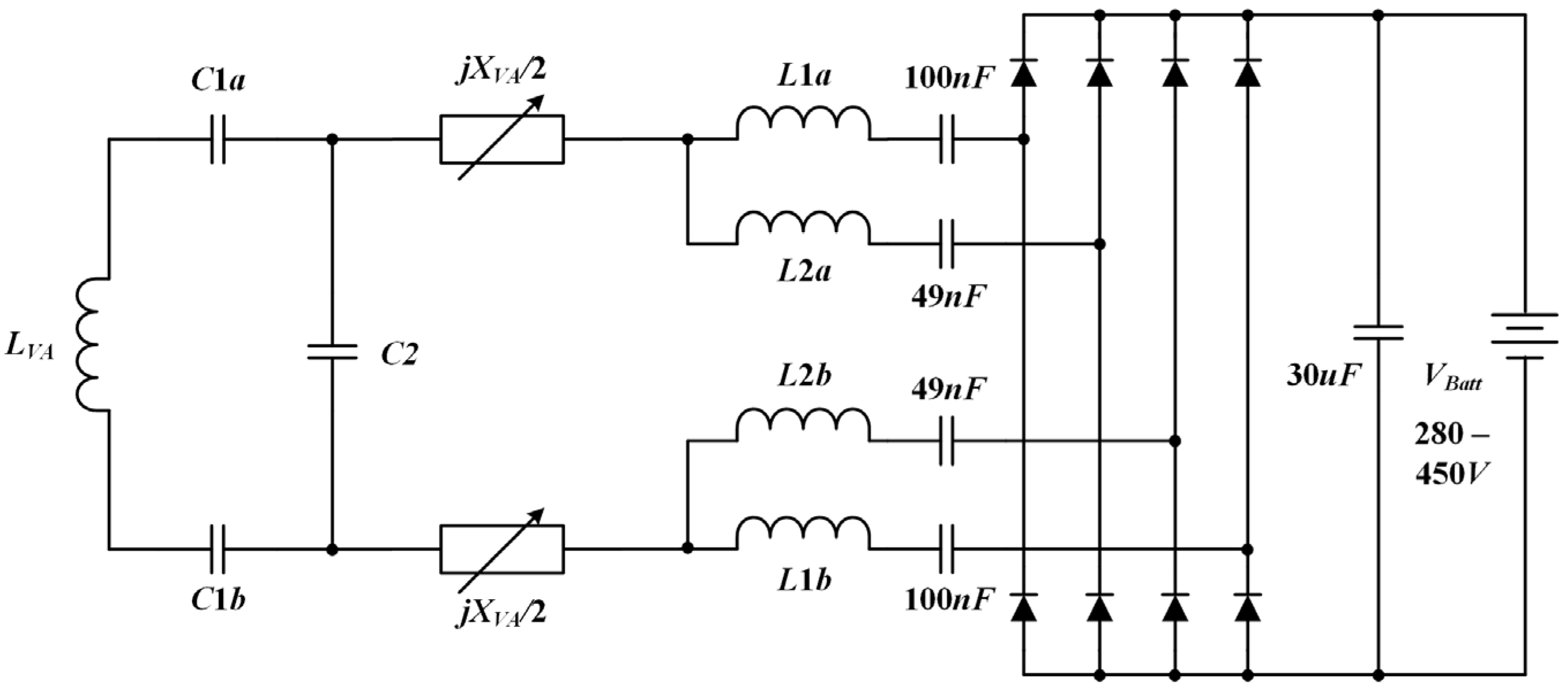
Figure 2 illustrates an example test station configuration recommended by SAE J2954. It supports an output voltage range of 280–450 V, which is suitable for charging 400 V class batteries. The key circuit components are listed in Table 1. Similarly, Figure 3 presents an example of a product circuit provided by SAE J2954 that supports an output voltage range of 280–420 V. This also confirms that the example circuit was designed for 400 V class battery systems. The inductance range and capacitor values used in this example are summarized in Table 2.

Figure 2.
Test station VA circuit in SAE J2954 standard [4].

Table 1.
Test station VA specifications in SAE J2954 standard [4].
Figure 3.
Example product VA circuit in SAE J2954 standard [4].
Table 2.
Example product VA specifications in SAE J2954 standard [4].
As shown, all WPT circuit topologies and design parameters referenced in the SAE J2954 appendix were optimized exclusively for 400 V battery systems. The direct application of these parameters to 800 V class battery charging faces two critical challenges.
- Output Voltage Limitations: The prescribed voltage ranges are insufficient to meet the requirements of 800 V battery packs.
- Excessive Component Stress: Even if the target charging voltage is achieved, the voltage and current stresses on the compensation circuit components (inductors and capacitors) become high, complicating practical implementation.
Thus, a redesigned WPT system that ensures compliance with the elevated output voltage and minimizes the stresses on the compensation network is imperative for 800 V class EVs.
3. Double-Sided LCC Compensation WPT System
3.1. System Configuration and Modeling
The double-sided LCC (DS-LCC) compensation network and its associated power-conversion components employed in this study are illustrated in Figure 1. Here, S1–S4 represent the MOSFETs on the transmitter side, and D1–D4 denote the diodes on the receiver side, where L1 and L2 correspond to the self-inductances of the GA-side and VA-side coils, respectively. The GA-side compensation components Lf1, Cf1, and C1 and the VA-side components LCf2, Cf2, and C2 form a resonant network, where M denotes the mutual inductance between the coils.
Although higher-order harmonic components are inevitably generated during the switching operation on the GA side for wireless power transfer, such components are significantly attenuated in loosely coupled WPT systems and, thus, can be reasonably neglected [24]. Therefore, in modeling the system, the proposed compensation network was simplified by analyzing only the fundamental component of the square voltage waveform at the switching frequency. The resistances of all inductors and capacitors are neglected for analytical clarity. The accuracy of this approximation is validated in later sections using circuit simulations and experimental results.
Typically, WPT system modeling is conducted based on the resonant operation. In the case of the DS-LCC compensated WPT system, the GA and VA sides exhibited a symmetrical structure; thus, identical resonance conditions occurred on both sides. Specifically, two types of resonances were observed: one between Lf1 and Cf1 (and, similarly, Lf2 and Cf2) and another between Cf1, C1, and L1 (similarly, Cf2, C2, and L2). When the system operates at resonance, the total impedance of each resonant loop becomes zero, thereby satisfying the condition expressed in Equation (1) below.
By rearranging Equation (1) with respect to the angular resonant frequency (ω₀), the DS-LCC compensation topology can be analyzed using the first harmonic approximation method under the resonant condition defined by Equation (2).
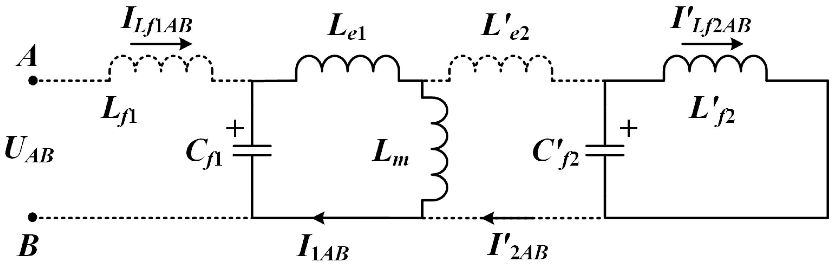
To optimize the design of a DS-LCC resonant network, it is critical to evaluate the voltage and current stresses imposed on the inductors and capacitors. This analysis was facilitated by representing the DS-LCC system as an equivalent transformer model, as shown in Figure 4, and applying the superposition principle. For simplicity, the resistances of all the inductors and capacitors were neglected. The accuracy of the approximate values derived from these equations was validated through simulations and experiments.
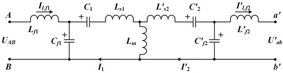
Figure 4.
Transformer equivalent model of double-sided LCC compensation structure.
The transformer equivalent model in Figure 4 is referred to as the primary model, in which the parameters can be derived using Equations (3)–(10).
In this model, UAB represents the input voltage applied to the compensation network, and Uab denotes the output voltage before the rectifier diodes. The terms L’s2, L’f2, C’2, C’f2, and U’ab correspond to the secondary-side resonant network components, which are referred to as the primary side.
Prior to analyzing the transformer equivalent model at ω₀, the series-connected elements Ls1, C1, L’s2, and C’2 were simplified into equivalent inductances Le1 and L’e2 using Equations (2), (5), and (6). This yields the simplified expressions in Equations (11) and (12):
To apply the superposition principle, the analysis must be performed separately for the input and output sides, followed by the calculation of the currents in each closed-loop circuit. First, to analyze the input side, the output terminals were short-circuited, as shown in Figure 5. Under these conditions, the transformer equivalent circuit comprises two loops. The sum of Le1 and Lm in the left loop, calculated using Equations (4) and (11), is equal to Lf1, thus forming a resonant circuit with Cf1. Consequently, the current through L’s2, denoted as Lf1AB, becomes zero. Similarly, the right loop, consisting of L’f2 and C’f2, also forms a resonant circuit, resulting in I’2AB = 0. The currents in each closed loop, I’1AB and I’Lf2AB, are derived as follows:

Figure 5.
Transformer equivalent model viewed from the input side.
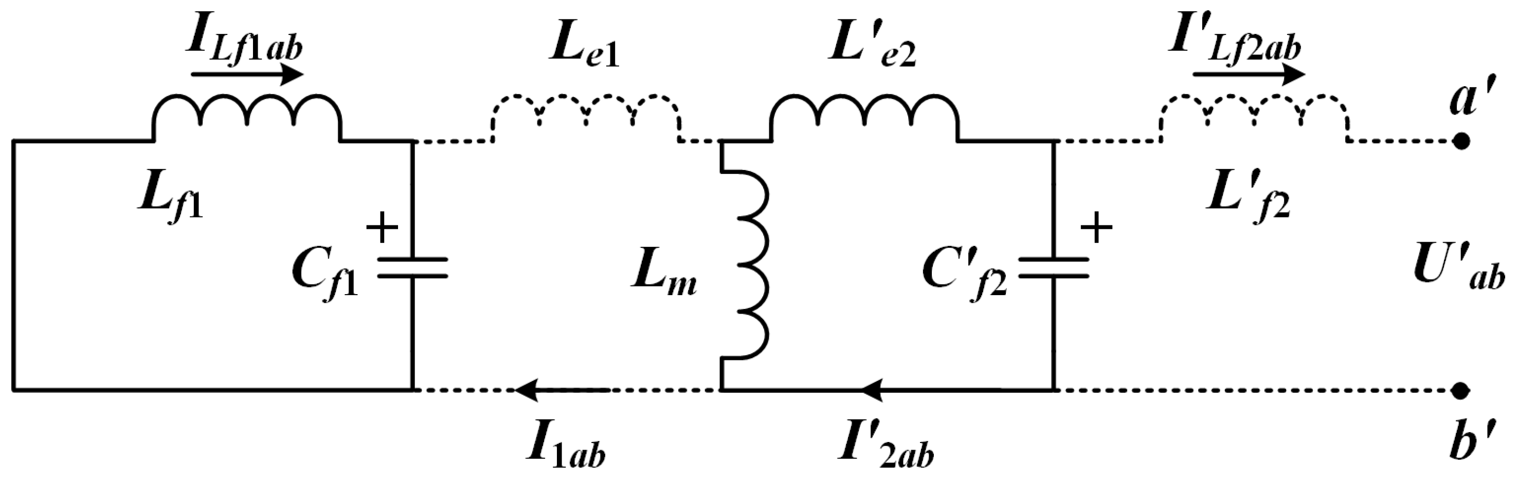
Next, to analyze the output side, the input terminals were short-circuited (Figure 6) and the currents in each closed loop were calculated analogously. In this case, I1ab and I’Lf2ab also become zero, and currents ILf1ab and I’2ab are expressed by Equations (15) and (16), respectively:
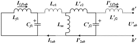
Figure 6.
Transformer equivalent model viewed from the output side.
Finally, the actual currents in the transformer equivalent resonant network were determined by summing the currents from the input- and output-side analyses. This yields the input/output currents and component-specific currents of the resonant network, as described by Equations (17)–(20). Equation (16) is derived using Equations (3), (7), (10), and (15), and Equation (20) follows an analogous formulation.
The currents through each component of the DS-LCC compensation circuit can be calculated using Equations (17)–(20) and Kirchhoff’s Current Law (KCL). The voltage stresses on the components are then determined based on their impedances and derived currents.
In this context, ILf2 corresponds to the current flowing through the AC equivalent resistance (Rac) in the AC equivalent circuit. Therefore, in order to calculate the actual output current (Iout) of the WPT system, the relationship for the AC equivalent resistance of a single-phase full-wave rectifier (as given in Equation (21)) is applied, leading to the expression shown in Equation (22).
A key insight from this analysis is that the DS-LCC compensated WPT system exhibits load-independent constant current (CC) characteristics when operating at the resonant frequency. Therefore, the output voltage is calculated as the product of the output current and the load resistance, which makes it highly sensitive to variations in the load resistance.
3.2. Optimal Design of Resonant Network
The key specifications of the 11.1 kW WPT system designed in this study are summarized in Table 3. The input voltage was set to 400 VDC, considering the output of the power factor correction converter, while the output voltage targets 800 VDC for compatibility with 800 V class battery systems. The resonant frequency of the WPT system was selected as 85 kHz, aligned with the SAE J2954 standard, which specifies a nominal power transfer frequency of 85 kHz within the allowable range of 79–90 kHz. To maintain a fixed operating frequency during the power transfer, the resonant network is designed to satisfy the target output characteristics by adjusting the capacitances in the compensation circuit.
Table 3.
System design key specifications.
While resonant networks in WPT systems generally comprise passive components (e.g., inductors and capacitors) with infinite combinations that satisfy the resonant frequency condition (Equation (1)), the design must account for frequency alignment as well as the voltage and current stresses on these components.
Table 3 lists the key parameters used in the system design. The input voltage was set to 400 V, assuming a typical grid voltage rectified using a conventional power factor correction (PFC) converter. The output voltage was set to a maximum value of 820 V to support the charging of high-voltage battery systems rated at approximately 800 V. The output power and switching frequency were determined according to SAE J2954 standards. Specifically, the WPT 3 class specification of 11.1 kW output power and a nominal switching frequency of 85 kHz were adopted. In this study, commercially available coils were used: the GA-side coil (L1) and the VA-side coil (L2), with inductance values of 35.67 μH and 111.42 μH, respectively. The system assumes ideal alignment between the GA and VA coils, with no lateral or angular misalignment. The vertical gap between the two coils was set to 150 mm.
To simplify the design process, the GA-side compensation inductance (Lf1) is derived analytically. At resonance, the input voltage and current of the WPT system are in phase, which enables the input power to be expressed as a product of these two quantities. Substituting the input current (ILf1) derived from Equation (16) into this power expression yields Equation (23). Rearranging Equation (23) for Lf1 results in Equation (24).
The VA-side compensation inductance (Lf2) is the sole independent variable in this formulation. Once Lf2 is selected, Lf1 is uniquely determined, and all the other component values (e.g., Cf1, C1, Cf2, and C2) can be derived using the resonant frequency condition (Equation (2)). This methodology confirms that infinite combinations of passive components satisfy the resonant frequency requirement.
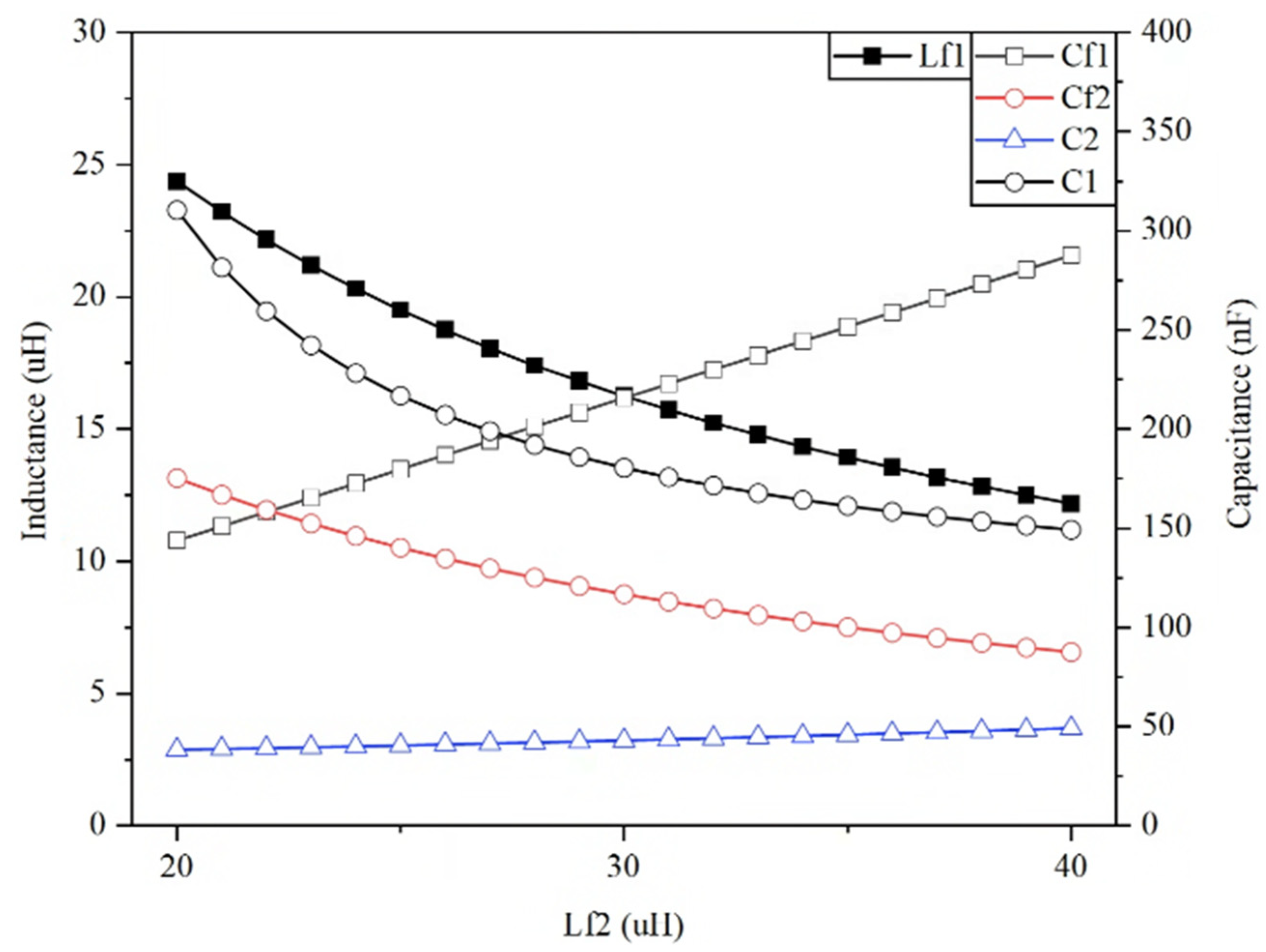
To design the resonant network, the VA-side compensation inductance Lf2 was varied within the range of 20–40 μH in 1 μH increments, and the resulting changes in the resonant network parameters were analyzed, as illustrated in Figure 7. As Lf2 increases, the GA-side compensation inductance (Lf1), series compensation capacitance (C1), and VA-side parallel compensation capacitance (Cf2) decrease. Conversely, the GA-side parallel compensation capacitance (Cf1) exhibits an increasing trend, whereas the VA-side series compensation capacitance (C2) shows a marginal increase.
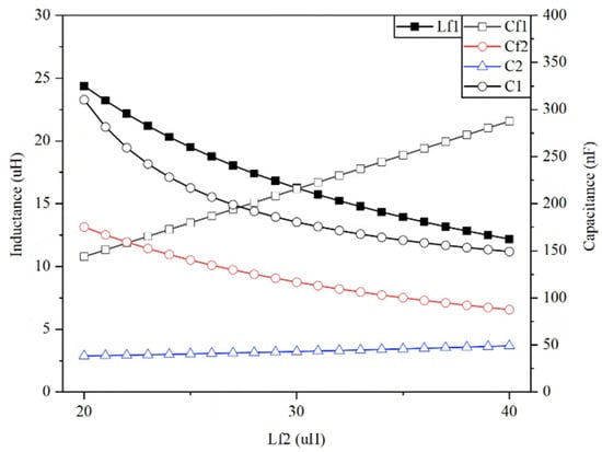
Figure 7.
Resonant network parameter changes according to Lf2 variation.
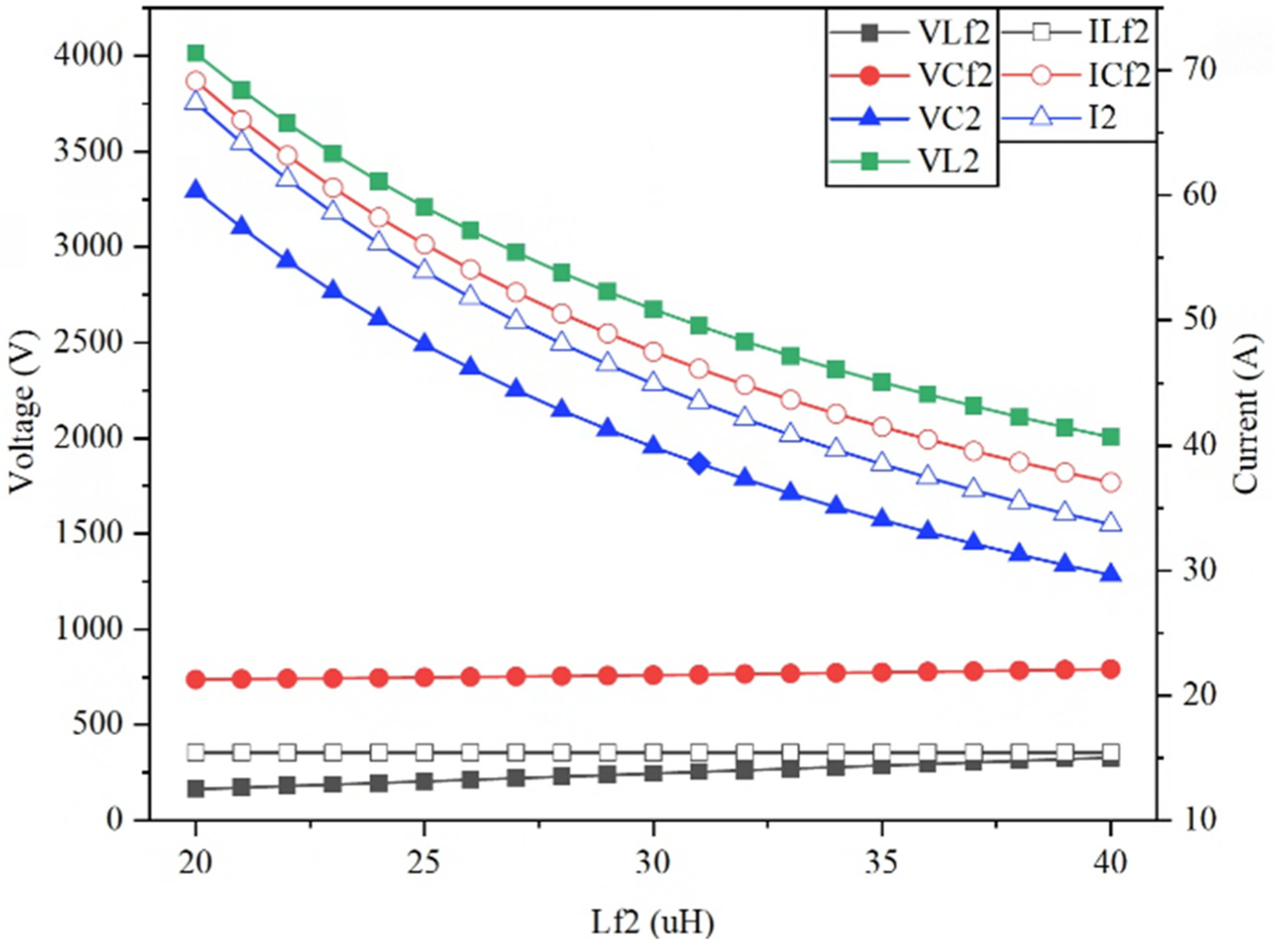
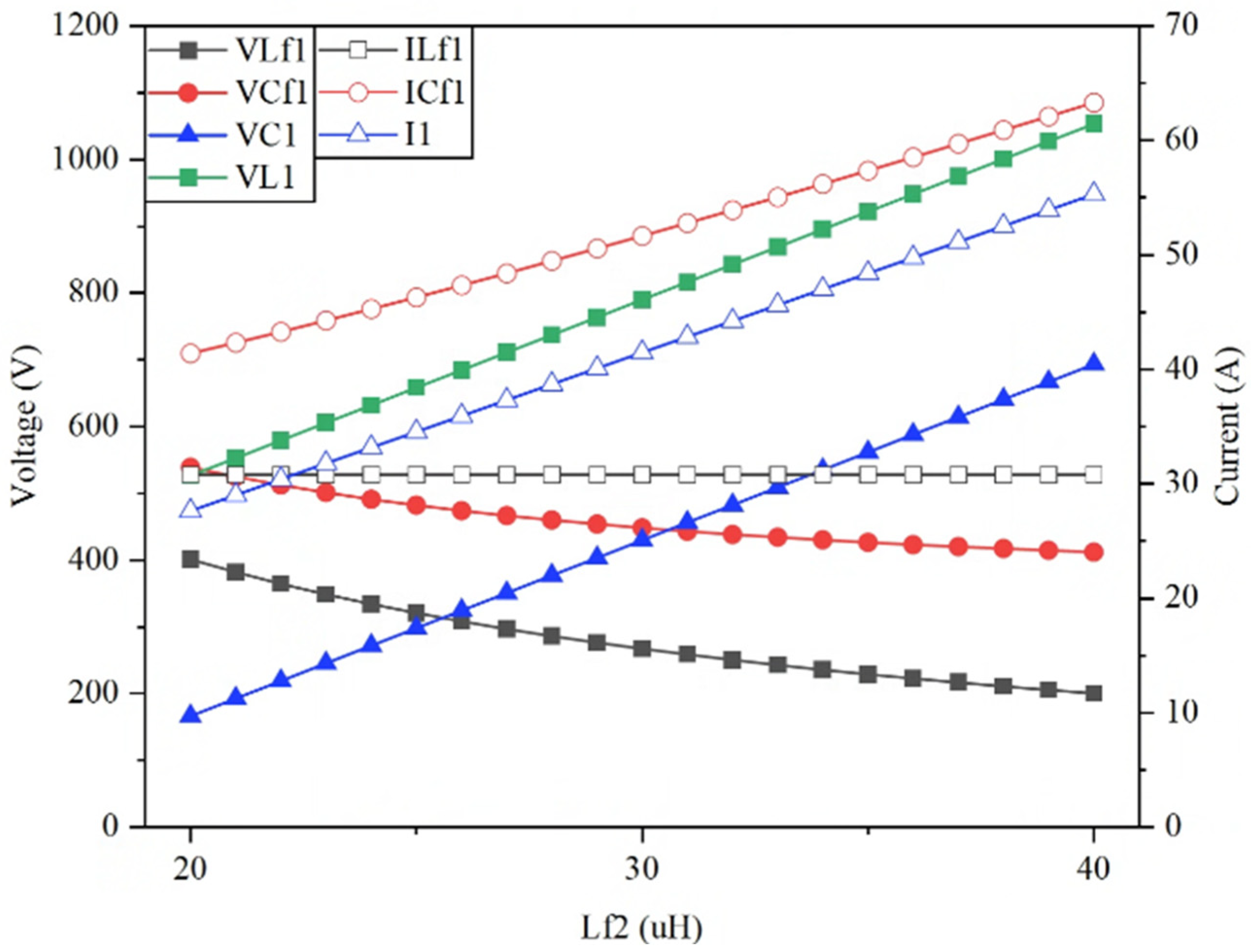
In practical implementation, adjusting the inductance values is relatively straightforward. However, compensation capacitors, often constructed using multilayer ceramic capacitor (MLCC) arrays in series-parallel configurations, pose manufacturing challenges when their required values become excessively large. In addition, high-voltage MLCCs exhibit a significant decrease in capacitance beyond a certain current threshold. Therefore, referring to the manufacturer’s datasheet is crucial to ensure that the current flowing through each individual capacitor in the series-parallel configuration does not exceed the level at which a substantial capacitance variation occurs. Thus, it is critical to evaluate the voltage and current stresses on the individual components to finalize the resonant network parameters. Figure 8 and Figure 9 show the voltage and current stresses on the GA-side and VA-side resonant network components, respectively, as functions of Lf2. These analyses provide a basis for selecting the optimal parameters that balance performance and manufacturability. As shown in Figure 8 and Figure 9, the voltage and current stresses on the resonant network components reached significant levels, spanning thousands of volts and tens of amperes, respectively. Notably, the magnitude of the stress varied across the components, depending on the configuration of the resonant network.
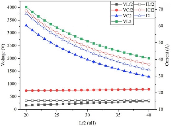
Figure 8.
GA-side resonant network voltage and current stress according to Lf2 variation.
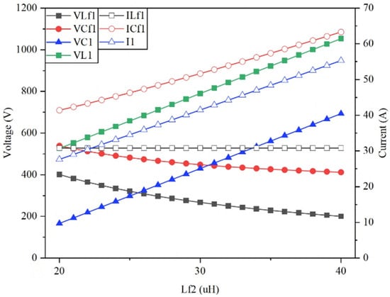
Figure 9.
VA-side resonant network voltage and current stress according to Lf2 variation.
In Figure 8 (GA-side stress analysis), the GA-side coil voltage (VL1) and series compensation capacitor voltage (VC1) increase as Lf2 increases. Concurrently, the parallel compensation capacitor current (ICf1) and the series compensation capacitor current, equivalent to the GA-side coil current (I1), also exhibit an upward trend.
Figure 9 (VA-side stress analysis) reveals a distinct behavior compared with the GA side. While the parallel compensation capacitor voltage (VCf2), compensation inductor voltage (VLf2), and inductor current (ILf2) show negligible increases with Lf2, the stresses on all other components decrease substantially. From a practical implementation perspective, the voltage stresses on the inductors or capacitors are relatively manageable. However, minimizing the current stresses is critical for reducing losses and simplifying the series-parallel configurations of capacitors, particularly when using MLCCs.
To balance these considerations, we selected Lf2 = 30 μH as the optimal VA-side compensation inductance. This value ensures a feasible resonant network design while accounting for real-world battery charging dynamics, which require additional operational constraints. Battery charging typically follows a constant current–constant voltage (CC-CV) profile. However, because the proposed WPT system lacks a dedicated battery management system (BMS) converter at the output stage, the voltage and current regulations must be directly integrated into the compensation network.
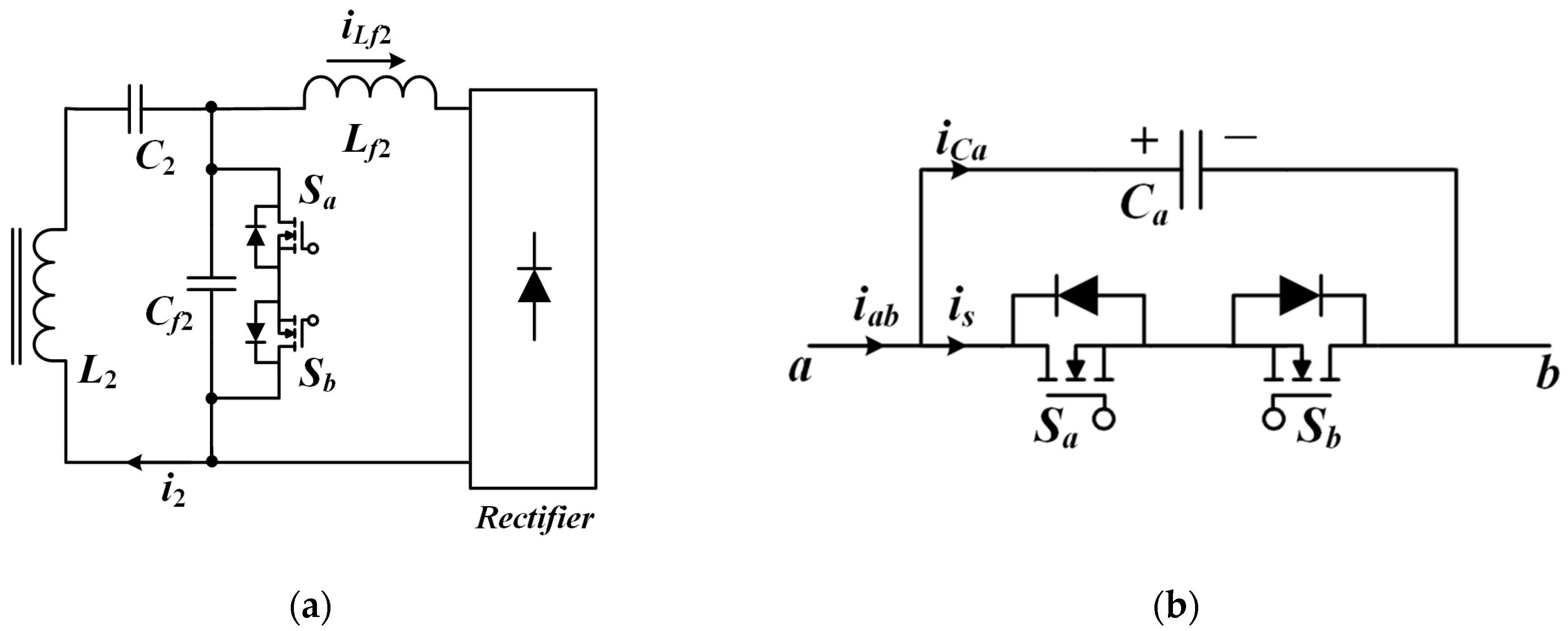
To this end, a switched capacitor scheme was applied to the parallel compensation capacitor (Cf2) on the VA side. The output voltage and current conditions could be regulated while maintaining a fixed operating frequency of 85 kHz by varying the effective capacitance of the parallel compensation capacitor (Cf2) through operation of the switched capacitor network.
Figure 10a shows the VA side of the WPT system with an applied switched capacitor circuit. Bidirectional MOSFETs connected in a back-to-back configuration were added parallel to the original VA-side parallel compensation capacitor (Cf2). Figure 10b illustrates a commonly used switched capacitor circuit, in which the effective capacitance (Ca) is adjusted based on the phase angle (α) between the control signals (Sa) and (Sb) [25].

Figure 10.
(a) VA-side circuit with a switched capacitor; (b) Switched capacitor circuit.
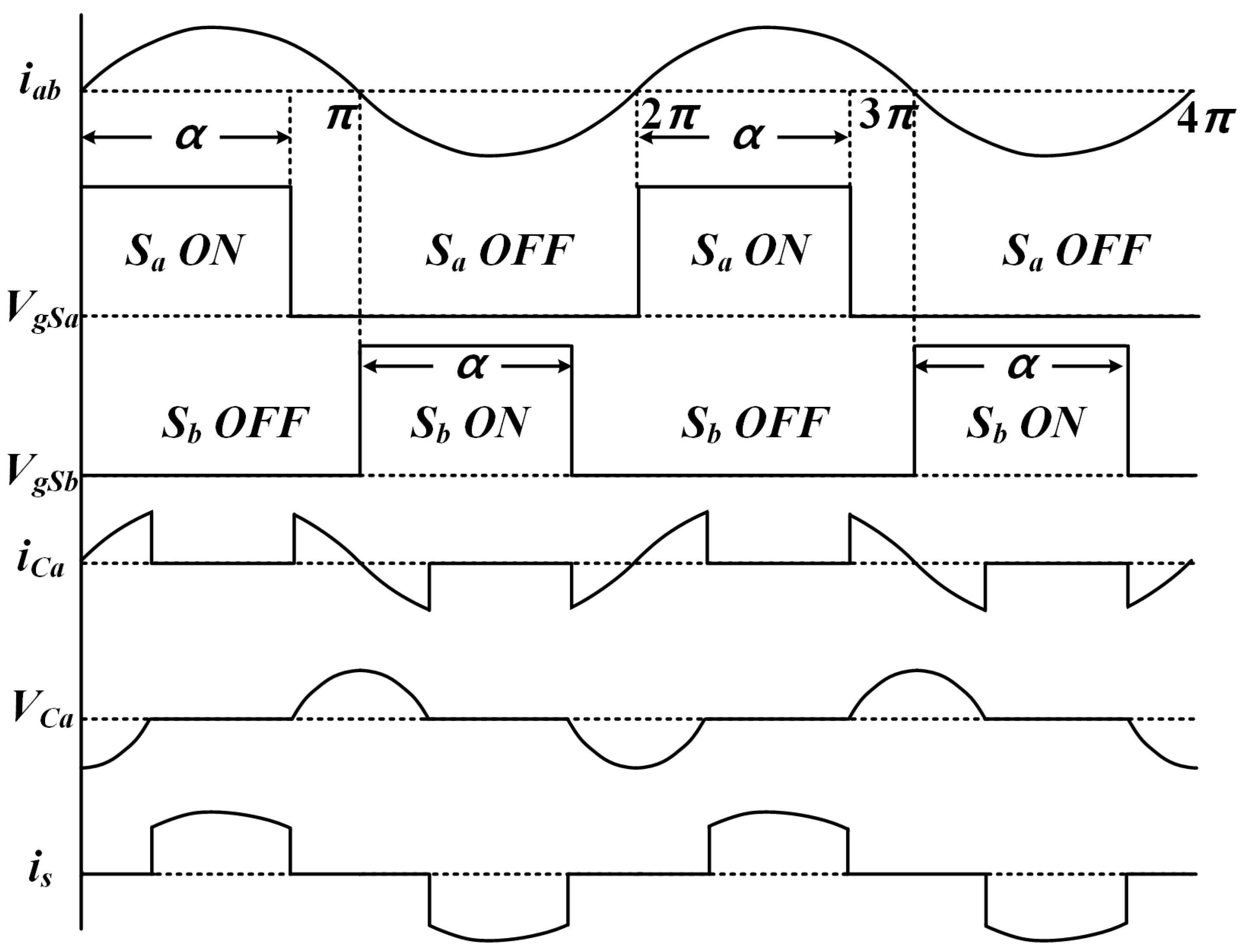
The operational waveforms of the switched capacitors are shown in Figure 11. The phase angle (α) of the switching control signal is adjustable within the range of π/2 to π. The equivalent capacitance (Ceq) of the switched capacitor, which can theoretically range from the nominal capacitance to infinity, is governed by Equation (25) [26].
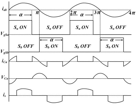
Figure 11.
Key waveform of switched capacitor circuit.
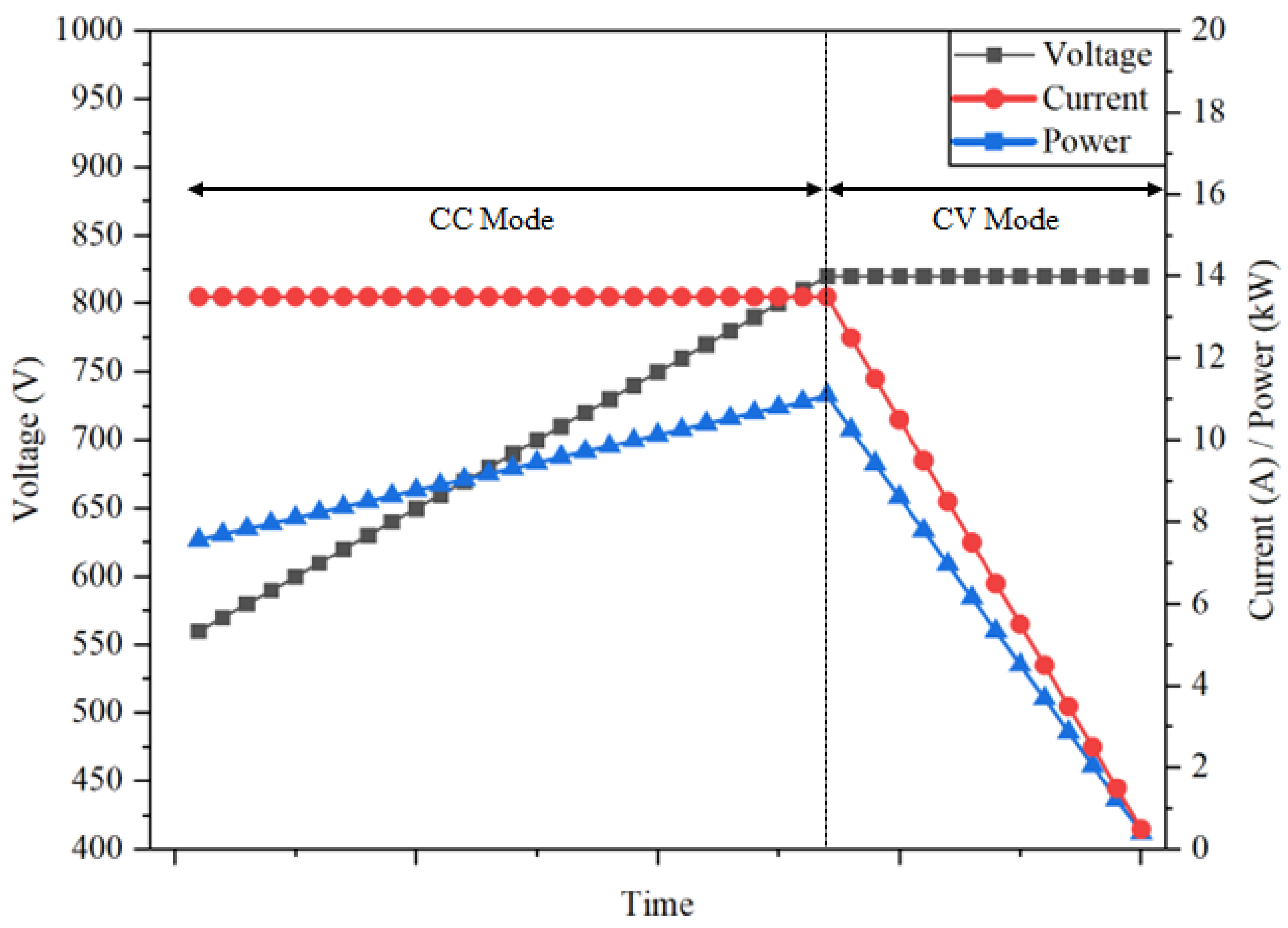
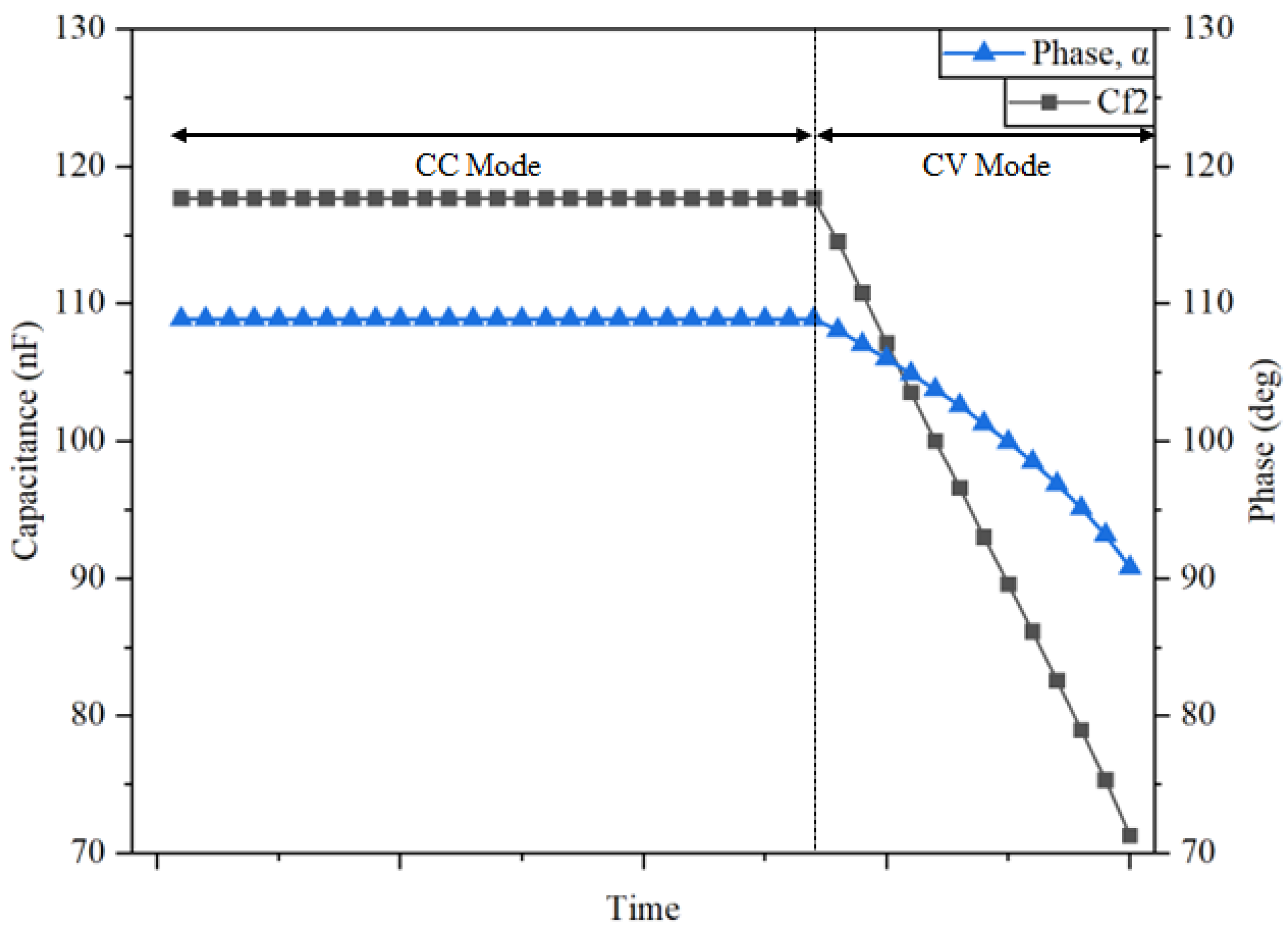
Figure 12 and Figure 13 illustrate the charging profile of an 800 V class battery over time and the corresponding variation in the key parameters of the switched capacitor used to regulate the charging process. As shown in Figure 12, in the initial stage, the system operates in constant current (CC) mode, charging the battery with a current of 13.5 A. As the charge state increases, the battery voltage increases. Once the battery voltage reaches 820 V, the system transitioned to the constant voltage (CV) mode, during which the charging current gradually decreases. Figure 13 illustrates the variations in the key parameters of the switched capacitor in response to the charging profile. The nominal value of the parallel compensation capacitor is set to 70 nF. During the CC mode, the phase angle (α) of the switched capacitor is maintained at 108.9 degrees, resulting in an equivalent capacitance of 117.7 nF, as calculated by Equation (22). This value corresponds to the resonant capacitance that achieves a resonant frequency of 85 kHz on the VA side. The phase angle (α) remains constant despite variations in load during the charging process because the DS-LCC compensated WPT system exhibits load-independent constant current characteristics when operating at resonance. After transitioning to CV mode, the equivalent resistance of the battery changes as charging progresses. The phase angle (α) of the switched capacitor is gradually reduced to maintain a constant output voltage of 820 V, which, in turn, causes the equivalent capacitance of the parallel compensation capacitor to decrease.
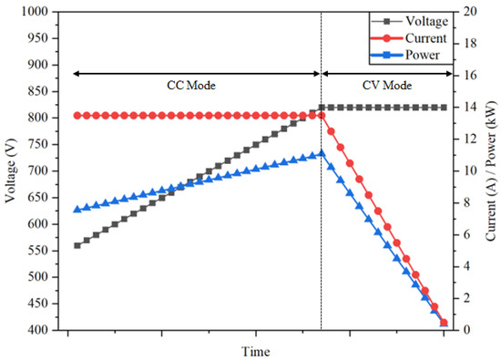
Figure 12.
Charging profile of 800 V class battery.
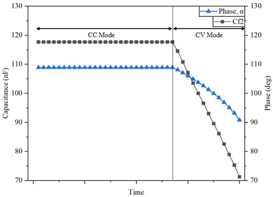
Figure 13.
Changes in key variables of switched capacitors according to battery charging.
Table 4 summarizes the final values of the resonant network parameters, derived from the design considerations discussed above.
Table 4.
Resonant network parameter.
4. Simulation and Experiment Results
4.1. Simulation Results
This section presents the validation of the feasibility of the double-sided LCC compensation network designed in Section 3 through a simulation. The key parameters of the simulation circuit, listed in Table 1 and Table 2, were used to analyze the resonant network configuration and verify the compliance with the battery charging profile under the switched capacitor operation of the VA-side parallel compensation capacitor (Cf2).
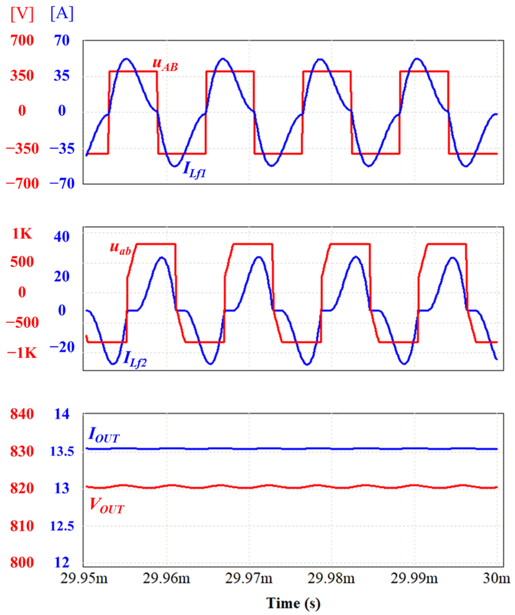
A simulation model was implemented using PSIM 12.0.3 to evaluate the performance of the proposed double-sided LCC-compensated WPT system. The input voltage was fixed at 400 VDC, and the load resistance was varied from 41 to 1640 Ω to emulate the battery charging profile. The resulting output voltage, current, and power characteristics were analyzed. The output voltage and current closely followed the target output characteristics. Specifically, the resonant network voltages and currents calculated at critical points, such as the start/end of charging and the CC-to-CV transition, were compared with the simulation results to confirm alignment. Figure 14 shows the typical operating waveforms of the double-sided LCC compensated WPT system, depicting the GA-side and VA-side voltages/currents at the CC-CV transition point. The voltage and current stresses on the resonant network components derived from the designed parameters were further verified through simulations.
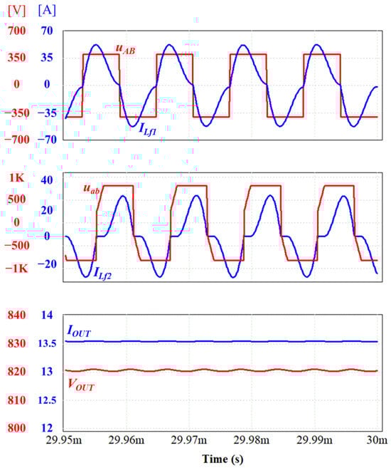
Figure 14.
Key simulation waveforms.
Based on the simulation results, the design validity of the double-sided LCC compensated WPT system was confirmed, and a hardware prototype was fabricated for experimental validation.
4.2. Experimental Results
A testbed was constructed to validate the operation of the designed resonant network, as shown in Figure 15. The air gap between the GA and VA coils was set to 150 mm, and a 40 μF capacitor (CO) was selected as the output filter. Each coil is connected to the input and output rectifiers through an LCC compensation network. A constant voltage electronic load was employed to emulate the battery, enabling precise voltage regulation. The specifications of the system used in the experiments are listed in Table 3. During the fabrication of the compensation circuit, minor discrepancies between the designed and actual component values were observed; however, these variations remained within a 1–2% tolerance range and exerted a negligible impact on the experimental outcomes.
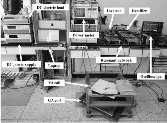
Figure 15.
Experimental setup of 11.1 kW WPT system.
The experimental setup replicates the circuit configuration shown in Figure 1. Wolfspeed’s SiC MOSFET (C3M0030090K) and SiC diode (E4D20120D) were utilized for the power switches, and all tests were conducted at an ambient temperature of 25 °C.
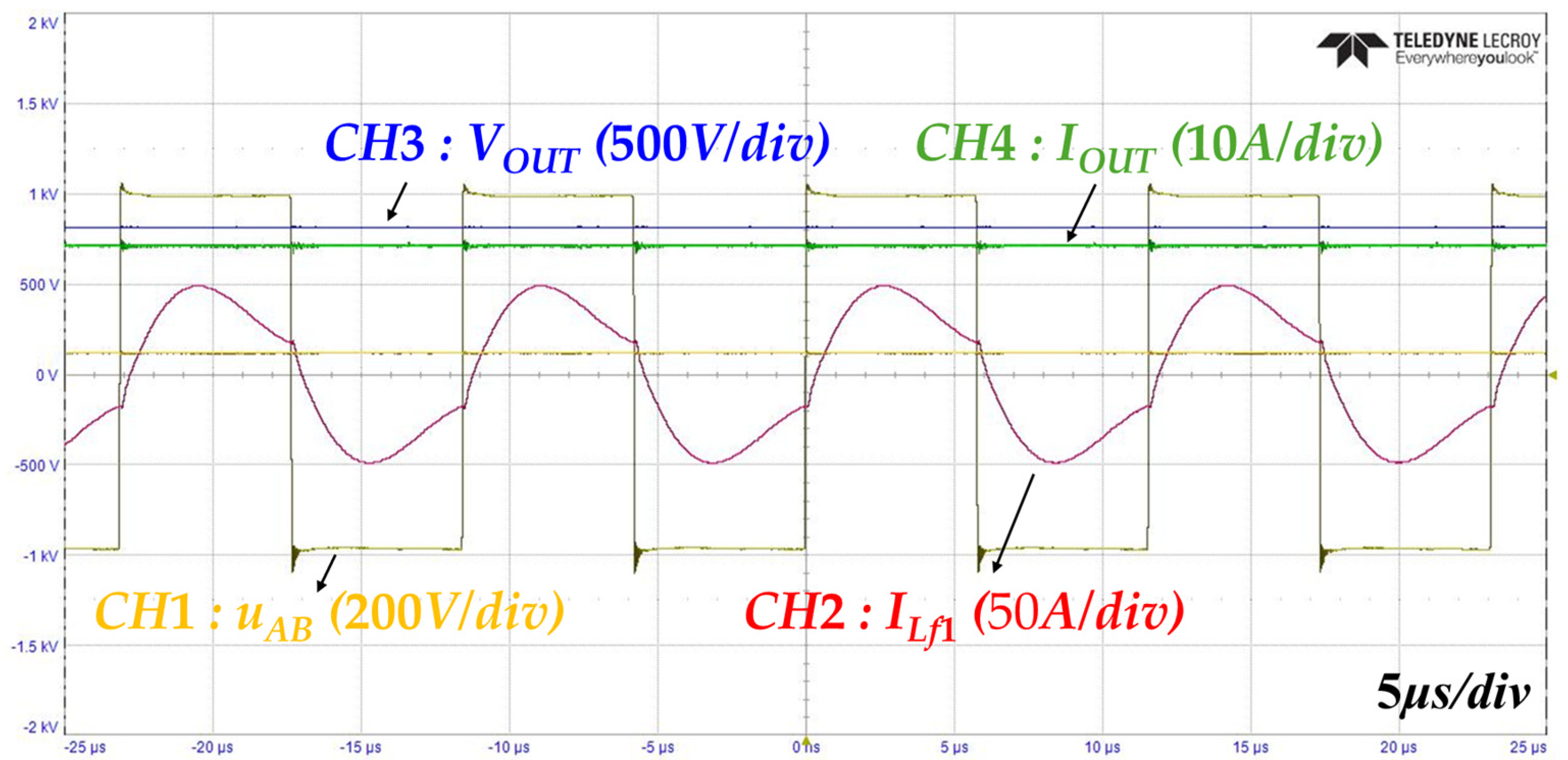
Figure 16 shows the steady-state waveforms of the DS-LCC compensated WPT system under normal operation. CH1 represents the GA-side pole voltage (uAB), and CH2 represents the GA-side pole current (ILf1). Here, CH3 and CH4 correspond to the output voltage (VOUT) and output current (IOUT), respectively. These waveforms were captured under output conditions of 800 V and 13.5 A, corresponding to the maximum power point (11.1 kW) in the battery-charging profile shown in Figure 12.
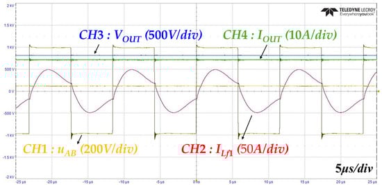
Figure 16.
Experiment setup of 11.1 kW WPT system.
The system efficiency, measured using a power analyzer (WT1800, Yokogawa Electric Corporation, Tokyo, Japan), reached 95% under full-load conditions. Table 5 compares the calculated and measured voltage/current stresses on the resonant network components at 11.1 kW. The maximum observed discrepancy was 8–9%, confirming the validity of the stress analysis methodology and the robustness of the resonant network design.
Table 5.
Voltage/current stresses on resonant network components at 11.1 kW.
5. Discussion
In this study, an optimal design of a double-sided LCC (DS-LCC) compensation network was proposed for an 11.1 kW wireless power transfer (WPT) system aimed at 800 V class battery charging. The simulated and experimental results demonstrated strong agreement with the analytically derived values in terms of the voltage/current stress and efficiency characteristics. A stable system operation was confirmed, and a maximum power transfer efficiency of 95% was achieved. These results reaffirm the critical role of the compensation network in WPT systems and suggest that the proposed design can serve as a valuable reference for the development of future high-voltage EV charging systems.
Furthermore, a comparison with previous studies summarized in Table 6 clearly highlights the contributions of this study. The approaches presented in [7,8] focus on the development of WPT systems capable of supporting both 400 and 800 V battery configurations. By contrast, the studies in [11,13,15] also target an 11.1 kW power level but adopt different resonant network topologies and are primarily intended for 400 V battery charging. While the works in [10,27,28,29,30,31] utilized a resonant topology similar to that proposed in this study, they differed in terms of the rated power and battery voltage specifications. Moreover, most of these studies emphasized system-level design and optimization, with limited attention given to the analysis of voltage and current stresses on the resonant components. Although some reports have demonstrated higher efficiency, such results often reflect the incorporation of additional design features, such as optimized transmitter and receiver pads. In future studies, efforts will be made to address these aspects and further enhance the overall system efficiency.
Table 6.
Comparison between this work and the existing work about WPT system for EV.
In accordance with the research objectives of this study, the proposed DS-LCC compensation network was evaluated under ideal alignment conditions and a fixed air gap of 150 mm. Consequently, a detailed analysis of the misalignment and air-gap variation was excluded. However, these factors are critical in real-world EV charging scenarios. As such, future research will quantitatively assess the impact of coil misalignment and air-gap variations on the system output characteristics and efficiency, with the goal of deriving more practical and robust design improvements.
6. Conclusions
This paper presents an optimal resonant network design for an 11.1 kW WPT system with a double-sided LCC compensation circuit, targeting 800 V class EV battery charging. To address the excessive voltage/current stresses caused by adapting 400 V class parameters to 800 V systems, a design methodology was developed to minimize the stresses while meeting the output requirements. By optimizing the resonant parameters and integrating a switched capacitor for dynamic CC-CV profile control, the system achieved 95% efficiency at 11.1 kW. Experimental validation under a 150 mm air gap confirmed stress discrepancies below 8–9%, ensuring reliability.
Author Contributions
Conceptualization, C.-M.K. and J.-S.K.; Data curation, C.-M.K.; Formal analysis, C.-M.K.; Funding acquisition, J.-S.K.; Investigation, C.-M.K.; Project administration, J.-S.K.; Resources, J.-S.K.; Software, C.-M.K.; Supervision, J.-S.K.; Validation, C.-M.K. and J.-S.K.; Visualization, C.-M.K.; Writing—original draft, C.-M.K.; Writing—review & editing, J.-S.K. All authors have read and agreed to the published version of the manuscript.
Funding
This work was supported by the Technology Innovation Program (No. 20024348) and funded by the Ministry of Trade, Industry & Energy (MOTIE, Republic of Korea).
Data Availability Statement
The data are available in a publicly accessible repository.
Conflicts of Interest
The authors declare no conflicts of interest.
References
- Okasili, I.; Elkhateb, A.; Littler, T. A Review of Wireless Power Transfer Systems for Electric Vehicle Battery Charging with a Focus on Inductive Coupling. Electronics 2022, 11, 1355. [Google Scholar] [CrossRef]
- Zhang, Z.; Pang, H.; Lee, C.H.T.; Xu, X.; Wei, X.; Wang, J. Comparative Analysis and Optimization of Dynamic Charging Coils for Roadway-Powered Electric Vehicles. IEEE Trans. Magn. 2017, 53, 9402106. [Google Scholar] [CrossRef]
- Fareq, M.; Fitra, M.; Irwanto, M.; Hasan, S.; Arinal, M. Low Wireless Power Transfer Using Inductive Coupling for Mobile Phone Charger. J. Phys. Conf. Ser. 2014, 495, 012019. [Google Scholar] [CrossRef]
- SAE Standard J2954; Wireless Power Transfer for Light-Duty Plug-In/Electric Vehicles and Alignment Methodology. SAE International: Warrendale, PA, USA, 2020.
- Wang, M.; Li, Y.; Zhang, W. Transitioning from 400 V to 800 V Battery Architectures for Enhanced Electric Vehicle Performance. IEEE Trans. Veh. Technol. 2020, 69, 1234–1242. [Google Scholar]
- Patel, S.; Kumar, D. Advantages of High-Voltage (800 V) Systems in Modern Electric Vehicles. In Proceedings of the IEEE International Conference on EV Technology, Online, 24–26 May 2021; pp. 45–50. [Google Scholar]
- Grazian, F.; Soeiro, T.B.; Bauer, P. Voltage/Current Doubler Converter for an Efficient Wireless Charging of Electric Vehicles with 400-V and 800-V Battery Voltages. IEEE Trans. Ind. Electron. 2023, 70, 7891–7903. [Google Scholar] [CrossRef]
- Vaddemani, G.P.R.; Karneddi, H.; Ronanki, D. A Single-Stage Reconfigurable Wireless Charger for 400-V and 800-V Electric Vehicle Battery Voltages. In Proceedings of the 2024 IEEE Applied Power Electronics Conference and Exposition (APEC), Long Beach, CA, USA, 25–29 February 2024; IEEE: Piscataway, NJ, USA, 2024; pp. 1181–1186. [Google Scholar] [CrossRef]
- Allali, N. Enhancing Wireless Charging for Electric Vehicles: Active Load Impedance Matching and Its Impact on Efficiency, Cost and Size. Electronics 2024, 13, 2720. [Google Scholar] [CrossRef]
- Yang, B.; Zhang, Y.; Zhu, C.; Sahoo, S.; Chen, Y.; Mai, R.; He, Z.; Blaabjerg, F. A Design Method to Minimize Detuning for Double-Sided LCC -Compensated IPT System Improving Efficiency Versus Air Gap Variation. IEEE Trans. Power Electron. 2024, 39, 1723–1737. [Google Scholar] [CrossRef]
- Gaona, D.E.; Jiang, C.; Long, T. Highly Efficient 11.1-kW Wireless Power Transfer Utilizing Nanocrystalline Ribbon Cores. IEEE Trans. Power Electron. 2021, 36, 9955–9969. [Google Scholar] [CrossRef]
- Wang, Y.; Jiang, C.Q.; Chen, C.; Wang, X.; Li, X.; Long, T. Design and Analysis of Inductive Power Transfer System Using Nanocrystalline Flake Ribbon Core. IEEE J. Emerg. Sel. Top. Power Electron. 2024, 12, 3334–3347. [Google Scholar] [CrossRef]
- Zhang, X.; Hao, C.; Dou, R.; Liu, S.; Zhao, L.; Zhang, P.; Yang, Q. Ferrite Pads Gap Thermal-Magnetic Evaluation and Mitigation for 11.1 kW Wireless Power Transfer. IEEE Trans. Magn. 2023, 59, 8600806. [Google Scholar] [CrossRef]
- Mohamed, A.A.S.; Shaier, A.A.; Metwally, H.; Selem, S.I. Interoperability of the universal WPT3 transmitter with different receivers for electric vehicle inductive charger. eTransportation 2020, 6, 100084. [Google Scholar] [CrossRef]
- Herceg, D.; Rajs, V.; Despotović, Ž.; Popadić, B.; Šiljegović, M.; Kiraly, Z.; Vizvari, Z.; Wizner, K.; Felde, I.; Odry, P.; et al. Double-Layer Coils Design for 11 kW Wireless Power Transfer. Electronics 2024, 13, 547. [Google Scholar] [CrossRef]
- Niu, S.; Zhao, Q.; Niu, S.; Jian, L. A Comprehensive Investigation of Thermal Risks in Wireless EV Chargers Considering Spatial Misalignment From a Dynamic Perspective. IEEE J. Emerg. Sel. Top. Ind. Electron. 2024, 5, 1560–1571. [Google Scholar] [CrossRef]
- Rajamanickam, N.; Abraham, D.S.; Alroobaea, R.; Abdelfattah, W.M. Foreign Object Debris Detection on Wireless Electric Vehicle Charging Pad Using Machine Learning Approach. Processes 2024, 12, 1574. [Google Scholar] [CrossRef]
- Niu, S.; Zhang, C.; Shi, Y.; Niu, S.; Jian, L. Foreign object detection considering misalignment effect for wireless EV charging system. ISA Trans. 2022, 130, 655–666. [Google Scholar] [CrossRef]
- Woo, D.-G. Optimal Design and Control Strategy of Inductive Power Transfer Charging System for Electric Vehicles. Ph.D. Thesis, Sungkyunkwan University, Seoul, Republic of Korea, 2015. [Google Scholar]
- Ahmed, M.; Salama, M.M.A.; Mohamed, A.A.S. A Review of Inductive Power Transfer: Emphasis on Performance Parameters, Compensation Topologies, and Coil Design Aspects. IEEE Access 2023, 11, 10868–10886. [Google Scholar] [CrossRef]
- Ahire, D.; Gond, V.; Chopade, J. Compensation Topologies for Wireless Power Transmission System in Medical Implant Applications: A Review. Mater. Today Proc. 2022, 49, 2758–2764. [Google Scholar] [CrossRef]
- Liu, Y. Compensation Topologies in Wireless Power Transfer Converters. Ph.D. Thesis, Department of Electronic and Information Engineering, Hong Kong Polytechnic University, Hong Kong, China, 2021. Available online: https://theses.lib.polyu.edu.hk/handle/200/11518 (accessed on 18 April 2025).
- Fu, M.; Tang, Z.; Ma, C. Analysis and Optimized Design of Compensation Capacitors for a Megahertz WPT System Using Full-Bridge Rectifier. IEEE Trans. Ind. Inform. 2019, 15, 95–104. [Google Scholar] [CrossRef]
- Niu, S.; Lyu, R.; Lyu, J.; Chau, K.T.; Liu, W.; Jian, L. Optimal Resonant Condition for Maximum Output Power in Tightly Coupled WPT Systems Considering Harmonics. IEEE Trans. Power Electron. 2025, 40, 152–156. [Google Scholar] [CrossRef]
- Wang, Y.; Li, Y.; Zhang, W.; Ma, L.; Lu, G.; Cheng, K.W.E. Switched-capacitor-based adaptive tuning for wireless power transfer systems. IEEE Trans. Power Electron. 2021, 36, 7321–7332. [Google Scholar]
- Zhu, H.; Zhao, C.; Deng, J.; Cheng, K.W.E. A variable capacitance technique using switched capacitors for resonant wireless charging. IEEE Trans. Ind. Electron. 2020, 67, 7433–7442. [Google Scholar]
- Wang, Y.; Zhao, S.; Zhang, H.; Zhu, C.; Mei, Y.; Jiao, N.; Lu, F. Compact Z-Impedance Compensation for Inductive Power Transfer and its Capacitance Tuning Method. IEEE Trans. Ind. Electron. 2023, 70, 3627–3640. [Google Scholar] [CrossRef]
- Lu, J.; Zhu, G.; Lin, D.; Wong, S.C.; Jiang, J. Load-independent voltage and current transfer characteristics of high-order resonant network in IPT system. IEEE J. Emerg. Sel. Top. Power Electron. 2019, 7, 422–436. [Google Scholar] [CrossRef]
- Vu, V.B.; Tran, D.H.; Choi, W.J. Implementation of the constant current and constant voltage charge of inductive power transfer systems with the double-sided LCC compensation topology for electric vehicle battery charge applications. IEEE Trans. Power Electron. 2018, 33, 7398–7410. [Google Scholar] [CrossRef]
- Wang, F.; Zhang, W.; Ye, L.; Guo, J.; Liu, K.; Do, H.T. A Design Method to Implement ZVS for Electric Vehicle Wireless Charging System With Double-Side LCC Compensation. IEEE J. Emerg. Sel. Top. Power Electron. 2021, 9, 3791–3801. [Google Scholar] [CrossRef]
- Nguyen, V.-T.; Vu, V.-B.; Gohil, G.; Fahimi, B. Coil-to-Coil Efficiency Optimization of Double-Sided LCC Topology for Electric Vehicle Inductive Chargers. IEEE Trans. Ind. Electron. 2022, 69, 11242–11252. [Google Scholar] [CrossRef]


Disclaimer/Publisher’s Note: The statements, opinions and data contained in all publications are solely those of the individual author(s) and contributor(s) and not of MDPI and/or the editor(s). MDPI and/or the editor(s) disclaim responsibility for any injury to people or property resulting from any ideas, methods, instructions or products referred to in the content. |
© 2025 by the authors. Licensee MDPI, Basel, Switzerland. This article is an open access article distributed under the terms and conditions of the Creative Commons Attribution (CC BY) license (https://creativecommons.org/licenses/by/4.0/).