Abstract
The AC-AC chopper converter, as a direct power conversion device without DC intermediate stages, has garnered significant attention due to its advantages of high efficiency and fast dynamic response. However, the voltage spikes induced by switching device turn-off transients (reaching 143% of the reference voltage) severely threaten system reliability, while traditional RC snubber circuit parameter design methods (e.g., empirical formula-based approaches) exhibit limited suppression effectiveness. To address this issue, this paper proposes an optimized parameter design method for RC snubber circuits in AC-AC chopper converters by establishing a turn-off transient energy transfer model to optimize snubber resistor and capacitor parameters. Experimental results from the prototype based on the TMS320F28335 digital controller demonstrate that the optimized method suppresses voltage spikes to <10% and, even under a 40% step load variation from the nominal value, maintains output voltage fluctuations stably below 5%.
1. Introduction
In the field of power electronics, AC–AC converters play a pivotal role in altering electrical energy conversion. Based on output frequency characteristics, their topologies can be categorized into two major classes: the first is frequency-converting converters, and the second is choppers that maintain input–output frequency consistency [1,2,3]. As a representative topology for same-frequency conversion, AC chopper converters eliminate the mandatory DC link energy storage stage inherent in traditional two-stage AC–DC–AC conversion structures. Instead, they achieve direct AC-domain energy conversion through high-frequency pulse width modulation (PWM) strategies [4]. This architecture offers several technical advantages: the omission of intermediate energy storage improves system efficiency by approximately 3–5% (typical value) [5], and it enables millisecond-level dynamic response characteristics [6]. Consequently, AC–AC chopper converters are widely applied in industrial drives, variable-frequency speed regulation, lighting control, and renewable energy grid integration. Among these, AC–AC chopper converters can further be classified into single-phase and three-phase systems, with the focus of this study being single-phase systems.
In the domain of AC–AC power conversion, typical voltage regulation technologies primarily encompass two major topological configurations: thyristor-based phase-controlled voltage regulation employing semi-controlled devices, and AC chopper voltage regulation utilizing fully-controlled power semiconductor devices. The first category relies on phase-controlled thyristor circuits, which achieve voltage regulation through a phase-shift triggering mechanism inherent to semi-controlled devices. The second category adopts AC chopper topologies incorporating fully-controlled devices such as IGBTs/MOSFETs. Thyristor-based voltage control modulates the fundamental voltage component via gate-triggering angle phase delay, offering advantages in simplicity, cost-effectiveness, and operational reliability [7,8,9]. However, this method exhibits significant drawbacks including pronounced harmonic distortion (with total harmonic distortion typically ranging 25–40%) and degraded power factor (commonly 0.6–0.8), both critically impairing power quality and system efficiency [10,11,12]. Furthermore, its relatively sluggish dynamic response (typically 100–200 ms) substantially limits applicability in modern industrial and power systems demanding high-performance and energy-efficient operation [13].
In contrast, AC–AC chopper converters regulate the effective value of the output voltage by adjusting the duty cycle of high-frequency switching devices (such as IGBTs or MOSFETs) within a switching period. This technology enables low harmonic distortion, high power factor, and fast dynamic response, making it more suitable for applications where stringent requirements for power quality, power factor, and voltage regulation precision are critical [14,15,16].
Conversely, AC–-AC chopper converters have been observed to generate voltage or current spikes during operation. This phenomenon can result in a series of adverse effects, including severe electromagnetic interference (EMI), overvoltage stress on devices, increased circuit power losses, poor contact reliability, and signal disturbances [17].
In order to address this issue, previous studies have proposed various methods to mitigate voltage spikes. These methods include optimizing PCB layout and incorporating snubber circuits. While optimizing PCB layout can reduce parasitic inductance to a certain extent, thereby decreasing the voltage spikes generated during the switching operation, its protective effect remains relatively limited [18].
When considering factors such as usability, simplicity, and cost-effectiveness, the integration of RC snubber circuits has emerged as a more viable solution. In [19], an innovative approach combining dual-port network analysis with exhaustive algorithms was proposed to enhance the accuracy of RC snubber circuit design. However, this method is highly dependent on parasitic parameters, involves significant computational complexity, and focuses primarily on suppressing oscillations rather than reducing voltage spikes.
In recent years, scholars have conducted numerous studies on voltage spikes and oscillation suppression in the switching process of power devices. In the context of RC snubber circuit optimization, reference [20] has been instrumental in suppressing the switching oscillations of SiC power modules through parameter optimization. However, its capacitive design has been found to exhibit limitations in terms of overvoltage suppression and lacks experimental verification. The third-order circuit model proposed in reference [21] introduces a parameter design method; however, it does not consider the impact of package and PCB parasitic inductance. The time-domain model developed in reference [22] improves the switching characteristics of SiC MOSFETs; however, the methodology is only applicable to half-bridge topology, and the parameter optimization is not sufficiently correlated with the physical parameters.
In the domain of control strategy innovation, the bi-directional LLC resonant converter control strategy proposed in reference [23] enhances system stability. However, this strategy suffers from incomplete implementation of soft-switching and the complexity of the strategy. Conversely, reference [24] reduces the current rate of change through gate signal modulation, which mitigates voltage spikes but increases the complexity of drive signal processing significantly. It is noteworthy that the novel topology and modulation strategy proposed in the AC–AC chopper converter in reference [25] does not directly target voltage spikes but rather enhances the system stability by improving the commutation process. In contrast, reference [26] systematically demonstrates the suppression effect of RC snubber circuits in DC–DC buck circuits on the parasitic parameters and voltage spikes and experimentally verifies its effectiveness. While these studies have made technical breakthroughs, there are generally too many model idealization assumptions, insufficient experimental validation, limited topology applicability, and high common problems such as high control complexity, which point the direction of improvement for subsequent studies.
Similar studies on DC snubber circuits are also found in references [27,28,29]. However, such research is primarily focused on DC converter applications, with limited consideration of high-frequency characteristics, signal waveforms, phase variations, and bidirectional current handling in AC circuits. Therefore, their applicability to AC circuits remains constrained.
Given the widespread voltage spike issues in AC–AC chopper converters during operation, while considering the limitations of existing research in addressing the effects of parasitic inductance and capacitance on snubber circuit design and the lack of sufficient experimental validation, this study focuses on the optimized parameter design of the converter’s RC snubber circuit. Through in-depth analysis of the AC–AC chopper converter’s topological structure, operational principles, and voltage spike formation mechanisms, this study proposes an RC snubber circuit parameter optimization method based on theoretical analysis. Experimental verification validated the effectiveness of this method in suppressing voltage spikes.
In light of the pervasive issue of voltage spikes in AC–AC chopper converters during operation and given the limitations of extant research in addressing the impact of parasitic inductance and capacitance in snubber circuit design, as well as the paucity of sufficient experimental validation, the present study focuses on the optimization design of converters. By conducting a thorough analysis of the operating principles, topology, and voltage spike formation mechanisms of AC–AC chopper converters, this study proposes an enhanced calculation formula for snubber circuit parameters. This study further optimizes the parameter selection method by incorporating the parasitic characteristics of power switching devices. Additionally, a small-signal model of the converter is established, allowing for stability and dynamic performance analysis in the frequency domain, and a differentiated control strategy tailored to various load scenarios is developed. Empirical validation substantiates the efficacy of the optimized snubber circuit design in suppressing voltage spikes, enhancing system efficiency, and bolstering stability. This design offers a viable solution for the design and optimization of related power electronic devices.
The main innovations of this study are as follows:
- (1)
- A novel snubber circuit parameter optimization method is proposed. Unlike conventional empirical formula approaches, it considers the comprehensive effects of stray inductance, switching device parasitic capacitance, and load characteristics. Through theoretical analysis and experimental verification, this method enhances voltage spike suppression capability.
- (2)
- The experimental section includes tests with various parameter combinations, systematically analyzing the specific impacts of snubber resistors and capacitors on voltage spikes and waveform distortion. This not only validates theoretical formulas but also summarizes the key design mechanisms for snubber circuits.
2. Topology of the AC–AC Chopper Converter
To reduce voltage spikes during switching, minimize system harmonics, and reduce electromagnetic interference, the AC chopper voltage regulation system typically incorporates a freewheeling circuit and a filtering circuit. The freewheeling circuit provides a current path when the switching device is turned off, preventing excessive reverse voltage from being generated due to the instantaneous interruption of current, thus reducing voltage spikes. The filtering circuit smooths the voltage waveform, removes high-frequency harmonics, and suppresses electromagnetic interference generated by switching operations, ensuring a more stable and low-noise output voltage.
Furthermore, the configuration of the freewheeling and filtering circuits contributes to the stabilization of the output voltage under variable load conditions. The enhanced reliability and immunity of these circuits is achieved through the precise design and optimization of the switching devices’ control timing. The snubber circuit employs a RC snubber circuit configuration, which exhibits low power consumption and contributes to enhancing the stability and reliability of the system.
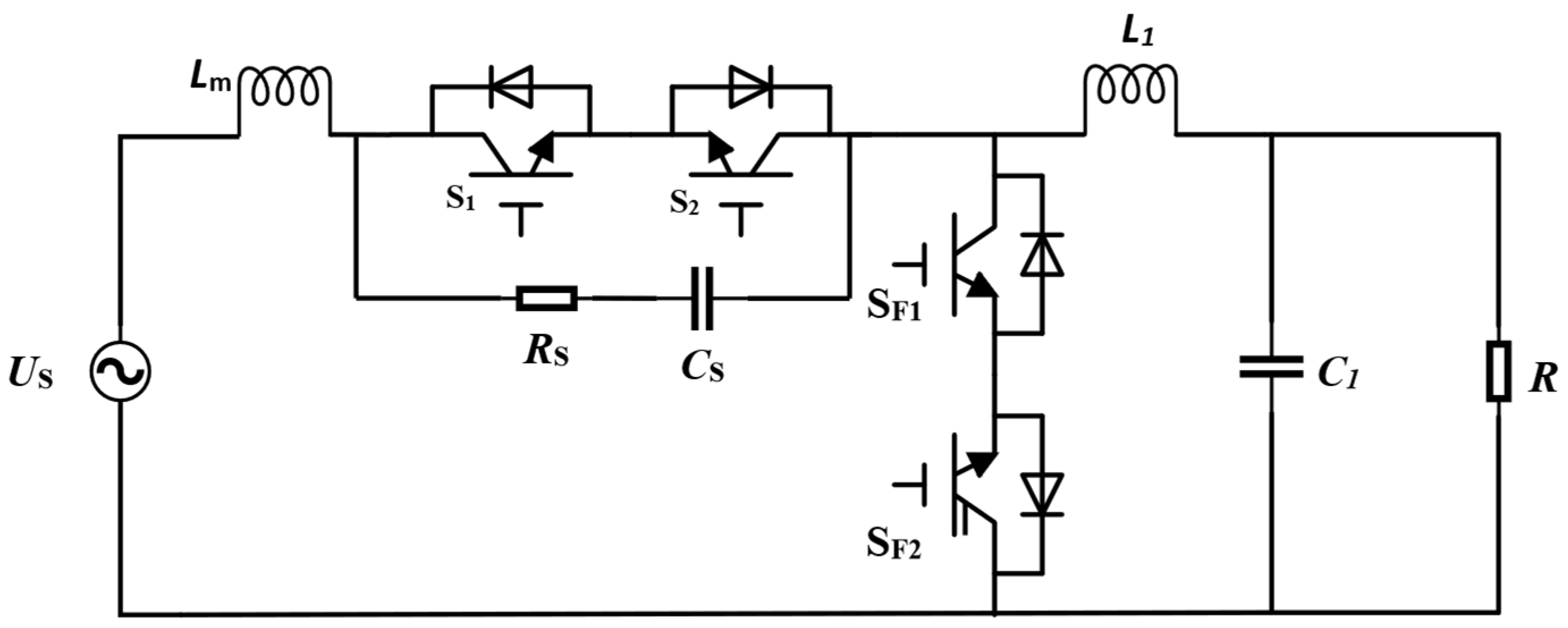
The topology of the designed AC–AC chopper converter is shown in Figure 1.

Figure 1.
Topology of the AC–AC chopper converter.
In the diagram, and , along with and , represent back-to-back IGBTs with anti-parallel diodes. and are the chopper switches, while and serve as the freewheeling switches. The RC snubber circuit is formed by and . represents the equivalent inductance resulting from the combined stray inductance in the circuit and the inductive load. The output of the device is a resistive load R, and the input is an AC voltage source . and form an LC filter.
3. Generation and Suppression of the Voltage Spike
3.1. Generation of the Voltage Spike in the AC–AC Chopper Converter
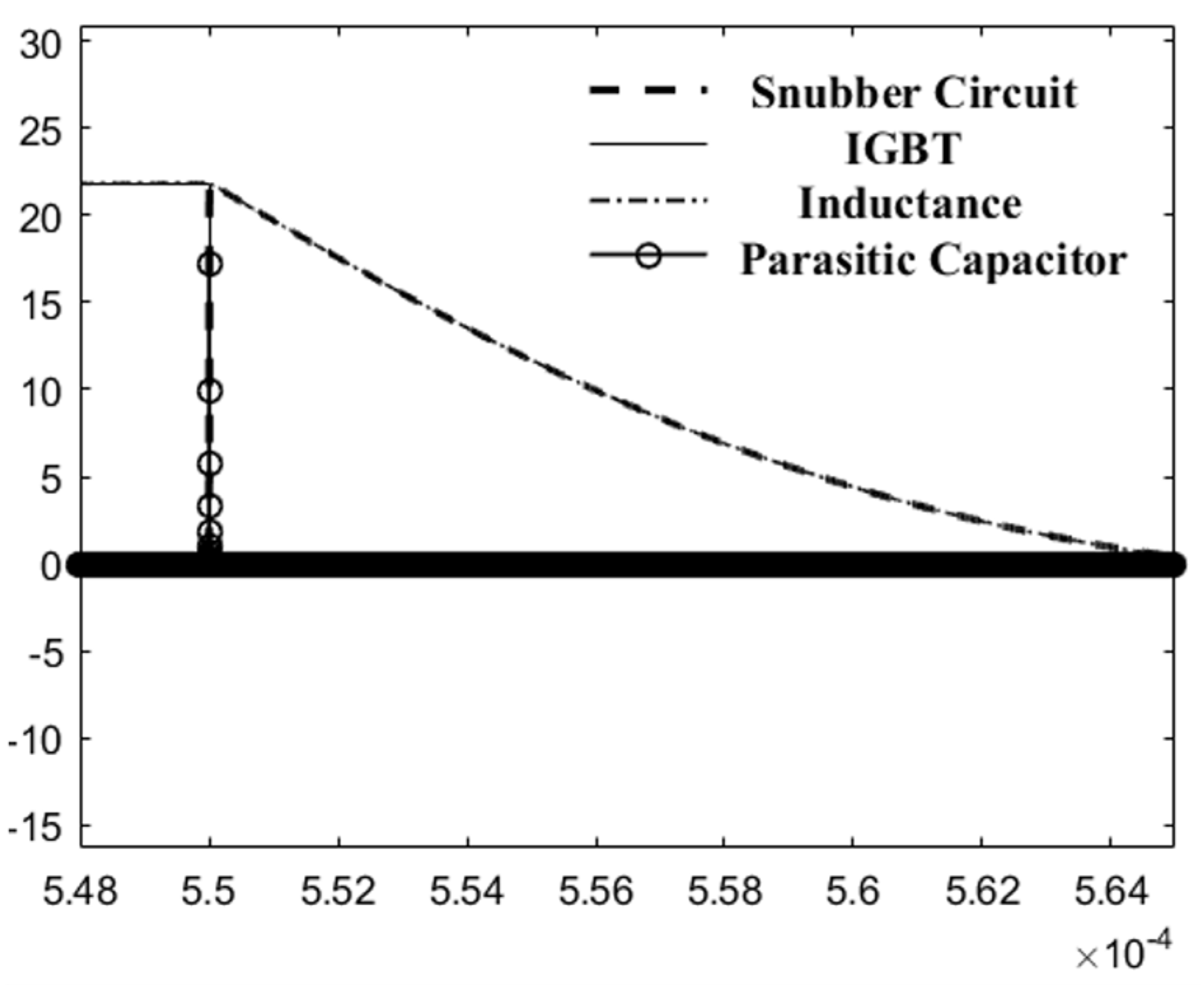
The reason for the voltage spike in the operation of AC–AC chopper converters is mainly due to the presence of stray inductors in the circuit. At the moment of switching device turn-on or turn-off, the current flowing through inductive components cannot change instantaneously, resulting in a substantial induced electromotive force from stray inductance, which consequently generates the voltage spike. This phenomenon is particularly pronounced at high chopper frequencies, when the load consists of low-resistance components, such as motors, and during the turn-off of power switching devices. The waveform of the collector current and the voltage between the collector and emitter is shown in Figure 2 when the IGBT is turning off.
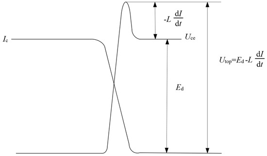
Figure 2.
Voltage spike when IGBT is turned off.
When the IGBT quickly turns off, the collector current quickly drops to 0, ignoring the leakage current. At this time, due to the presence of stray inductance in the main circuit, the current cannot suddenly change, resulting in a large impulse voltage . The large impulse voltage is combined with the power supply voltage to form the voltage spike .
Excessive voltage spikes can cause breakdown and damage to power devices such as MOSFETs, IGBTs, and thyristors, as these components have defined breakdown voltage and current limits. The spikes can also stress inductive loads like motors, leading to winding damage and insulation failure, which affects equipment reliability and operation. Furthermore, voltage spikes introduce harmonic distortion into the power system, reducing the power factor, causing system instability, and decreasing energy efficiency.
3.2. Analysis of the Working Condition of the AC-A–C Chopper Converter with Snubber Circuits
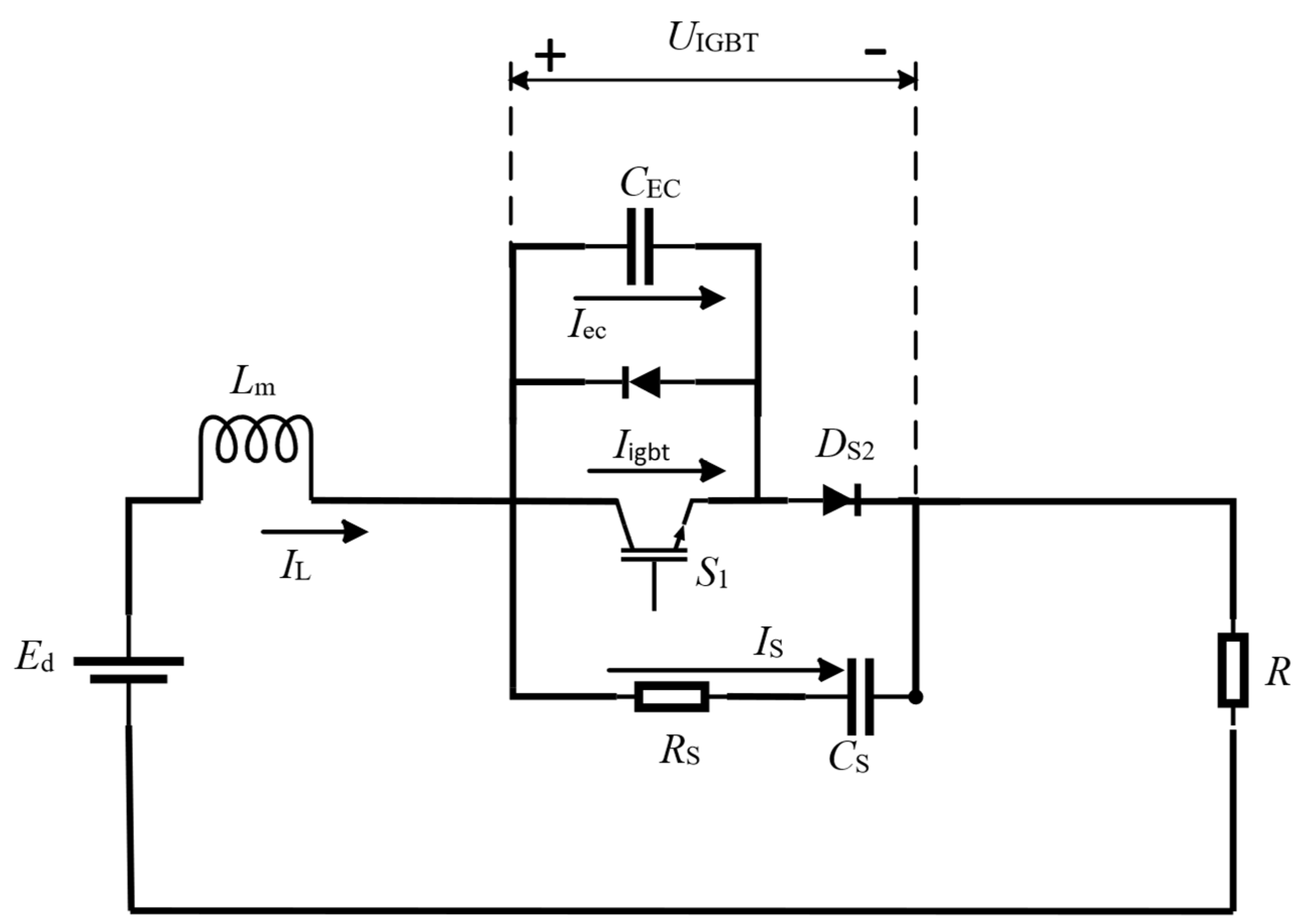
Given the relative complexity of the IGBT structure, it can be simplified in operational analysis: when turned on, the IGBT is approximated by a low-resistance equivalent (), and when turned off, it is represented by a high-resistance equivalent (), with the freewheeling diode effect neglected ( is defined as the turn-off time of the IGBT).
Since the voltage spike occurs over an extremely short duration, the circuit can be analyzed as a transient process. In this case, the input power supply is assumed to have a peak voltage of , with IGBT operating as a chopper and IGBT remaining continuously on. For simplification, the effect of the freewheeling circuit is neglected. Additionally, the parasitic capacitance between the emitter and collector terminals of the IGBT is introduced into the model to more accurately reflect the dynamic characteristics of the IGBT.
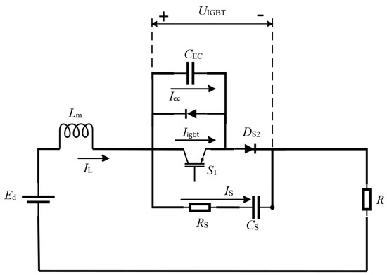
Figure 3.
Simplified topology of the AC–AC chopper converter.
For convenience in calculations, the parallel impedance of , the IGBT, and the snubber circuit is represented by .
Here, is the capacitance of the parasitic capacitor between the emitter and collector of the IGBT, is the capacitance of the snubber capacitor, and and represent the impedances of the IGBT and the snubber resistor.
Here, represents the current through inductor , and denotes the voltage across the snubber capacitor. and are the initial current of inductor and the initial voltage of snubber capacitor at the moment when the circuit switches states (on/off). is the snubber circuit current.
When the IGBT is turned off, the current and voltage waveforms for each part are shown in Figure 4 and Figure 5, respectively.
Figure 4.
Current transition during IGBT turn-off.
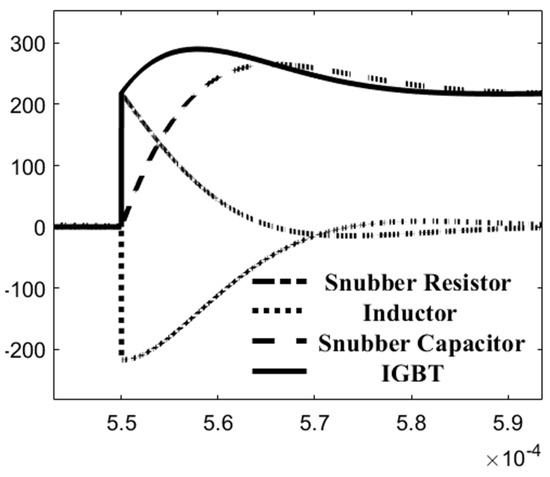
Figure 5.
Voltage transition during IGBT turn-off.
At the moment when IGBT turns off, the current through the inductor cannot change abruptly. Therefore, the inductor initially maintains the current flowing through the main circuit. At this point, the inductor generates an induced electromotive force as shown in Formula (5).
The current in the circuit flows out from the positive terminal of the power supply , passes through the stray inductance , and then splits into three parts. The resulting expression can be obtained as follows (6):
- 1.
- Current flows through the snubber circuit.
A portion of the current enters the snubber circuit, flowing through the snubber resistor and the snubber capacitor . At this moment, the snubber current rapidly rises until it equals the inductor current of , while the voltage that drops across the snubber resistor increases sharply. The snubber capacitor begins to absorb the energy released by the induced electromotive force generated by the inductor and the supply voltage . As a result, the voltage across the snubber capacitor continuously rises until it stabilizes at .
- 2.
- Current flows through IGBT parasitic capacitor .
The second part of the current flows into the parasitic capacitance of IGBT . At the instant when turns off, due to the rapid change in , the current through the parasitic capacitance rises sharply, with its magnitude determined by the capacitor current Formulas (7). Subsequently, rapidly decays to zero.
- 3.
- The current flows through IGBT .
The third part of the current flows directly through IGBT . When turns off, its equivalent resistance becomes extremely large, causing the current through to drop to nearly zero almost instantaneously. However, due to the continuity of the inductor current in , the induced electromotive force causes the voltage to rise rapidly.
Initially, the voltage across rises to the input supply voltage , but due to the presence of the induced electromotive force, the voltage further increases, forming a spike voltage .
Subsequently, the three current components merge again in the circuit and flow through the load resistance R. Ultimately, as the inductor current gradually decreases, the induced electromotive force attenuates, the voltage across the snubber capacitor stabilizes at , and the IGBT voltage also drops back to . The circuit transitions into a steady state, with the inductor energy fully released, marking the end of the transient process.
3.3. Calculation of Snubber Circuit Parameters
After the IGBT turns off, the snubber circuit current rises rapidly and gradually match the waveform of the main circuit current . At this moment, since the initial voltage of the snubber capacitor is zero, the charging current of the capacitor at the beginning of the snubbing process primarily depends on the circuit’s dynamic characteristics.
When the IGBT transitions from the on state to the off state, because the snubber circuit needs to gradually take over the main circuit current , the current of the snubber circuit will rise rapidly in a short time but is still smaller than the main circuit steady state current at the time of conduction, obtaining (9) and (10). This is mainly due to the parasitic parameters in the snubber circuit (e.g., snubber resistance and inductance) that limit the instantaneous rate of change of current.
Substituting Formula (9) into Formula (10) yields Formula (11).
From this, the first constraint condition for can be derived:
It is imperative to note that the snubber resistor resistance must not exceed the load resistance R. This is primarily to ensure optimal impedance matching between the snubber circuit and the load. Conversely, when the snubber resistor resistance value exceeds the load resistance value R, the impedance of the snubber circuit is excessively high, which will result in delayed energy return. Consequently, the transfer of energy between the snubber circuit and the load is impeded, impeding the circuit’s capacity to distribute and regulate energy in a timely and efficient manner.
When designing the snubber circuit, the selection of the snubber capacitor is crucial. The primary function of the snubber capacitor is to absorb the transient energy caused by the back electromotive force generated by the inductor when the IGBT turns off. This reduces the peak voltage magnitude and protects the switching device.
The energy stored in the inductor at the moment of turn-off is given by
The energy that the snubber capacitor needs to absorb can be expressed as
Since the main role of the snubber capacitor is to absorb the induced electromotive force caused by the stray inductance, its absorption capacity must exceed the energy of the induced electromotive force:
To ensure the snubber capacitor fully absorbs and releases the energy during each turn-off of the IGBT and to minimize the peak voltage, we assume
Substituting into Formula (15), we obtain
So
The design of the snubber capacitor must achieve a balance between absorbing voltage spikes, protecting switching devices, and maintaining the circuit’s dynamic performance. Its actual value should be slightly greater than the theoretical minimum to ensure sufficient absorption of the energy released by the inductor and to smooth the voltage waveform.
If is too large, it will result in increased energy losses, reduced system efficiency, and slower response of the snubber circuit to transient voltage spikes, making it unable to suppress high-frequency oscillations or overvoltage effectively. Therefore, selecting appropriately can effectively balance spike voltage suppression, dynamic performance, and energy loss, improving the circuit’s stability and efficiency.
In the AC–AC chopper converter, where the chopper frequency is relatively high, the minimum adjustable voltage is typically set to 10% of the input voltage. Under these conditions, the high-level duty cycle of the IGBT is only 10% of the entire chopping period. Therefore, the snubber circuit must respond quickly to absorb the energy released by the inductor .
The response speed of the RC snubber circuit is determined by its time constant τ. It is generally necessary to design the time constant of the snubber circuit to be sufficiently small to ensure a rapid response to changes in high-frequency chopper signals. According to the characteristics of RC circuits, a signal reaches approximately 95% of its final value after about three times constants.
To ensure that the snubber circuit can quickly reach a steady state during the high-level duration of the duty cycle signal, the time constant τ must satisfy the following condition:
Here, f is the frequency of the chopper signal.
The second constraint condition for can be obtained as follows:
This can be seen in conjunction with (12) and (20):
If the snubber resistor is too small, it will cause the transient current to increase significantly, particularly at the moment when the IGBT turns off. This leads to higher power losses in the snubber circuit, reducing system efficiency. Additionally, the snubber resistor will experience a high thermal load, potentially resulting in overheating, damage, and reduced system reliability. Moreover, the large transient current can cause electromagnetic interference (EMI), increasing high-frequency noise, which may disrupt the operation of other circuits and degrade signal quality. Therefore, the design of must strike a balance between limiting voltage spikes and controlling power losses. Its actual value should be slightly less than the theoretical value derived from Formula (21).
In theoretical analysis and simulations, the turn-off time of the IGBT is often neglected, leading to the assumption that the voltage spike occurs instantaneously. However, in practical applications, a specific condition may arise where the RC snubber circuit can completely release its energy within the IGBT turn-off time .
In the case of satisfying the Formula (12), the value of the snubber capacitor can be smaller than the theoretical calculated value while still effectively suppressing the voltage spike. The core of this strategy lies in using a small capacitance and a fast response design, allowing the snubber circuit to absorb and release energy during the brief turn-off time of the IGBT, achieving a smoothing effect on the voltage spike. This method is suitable for applications with high-frequency chopping or demanding dynamic performance, offering certain advantages.
However, it should be noted that the small capacitance design may have limitations under certain complex conditions (such as load fluctuations or strong parasitic effects). Therefore, in practical applications, simulation and experimental verification are still necessary to ensure that the snubber circuit meets dynamic performance requirements while maintaining good reliability and efficiency.
In summary, when the time constant and the snubber resistance , the value of the snubber capacitor can be slightly larger than the theoretical calculated value , or it can be appropriately reduced to a value much lower than this, as long as the snubber circuit meets the dynamic response speed requirements and effectively suppresses the voltage spike.
When , then
4. Design of Control Scheme for the AC–AC Chopper Converter
In the AC–AC chopper converter, different load types (such as purely resistive, inductive-resistive, and capacitive-resistive loads) impose varying requirements on control strategies and timing design. Its control timing diagram is shown in Figure 6.
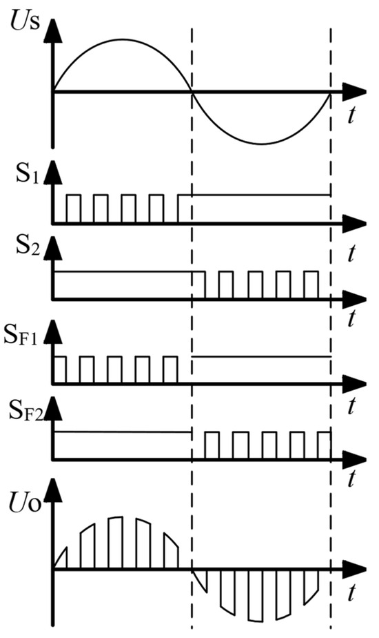
Figure 6.
Control timing diagram of the AC–AC chopper converter.
In complementary control mode, switches in different branches must alternate conduction while maintaining an interlock state. However, due to the inherent delay in the turn-on and turn-off times of switching devices, there is a risk of simultaneous conduction (common-state conduction), which can compromise system safety. Proper dead-time configuration is critical in complementary control. However, an overly long dead time reduces voltage regulation efficiency, while an overly short dead time cannot effectively prevent short-circuit risks.
When = 0, turns off, causing the load current to drop to zero, which also reduces the output voltage to zero. A similar principle can be applied to derive the output voltage waveform during the negative half-cycle. In the negative half-cycle, remains off, while and remain continuously on. Switch acts as the chopping switch and operates according to the duty cycle signal, with its operation logic being symmetric to that of the positive half-cycle.
5. Experimental Results and Analysis
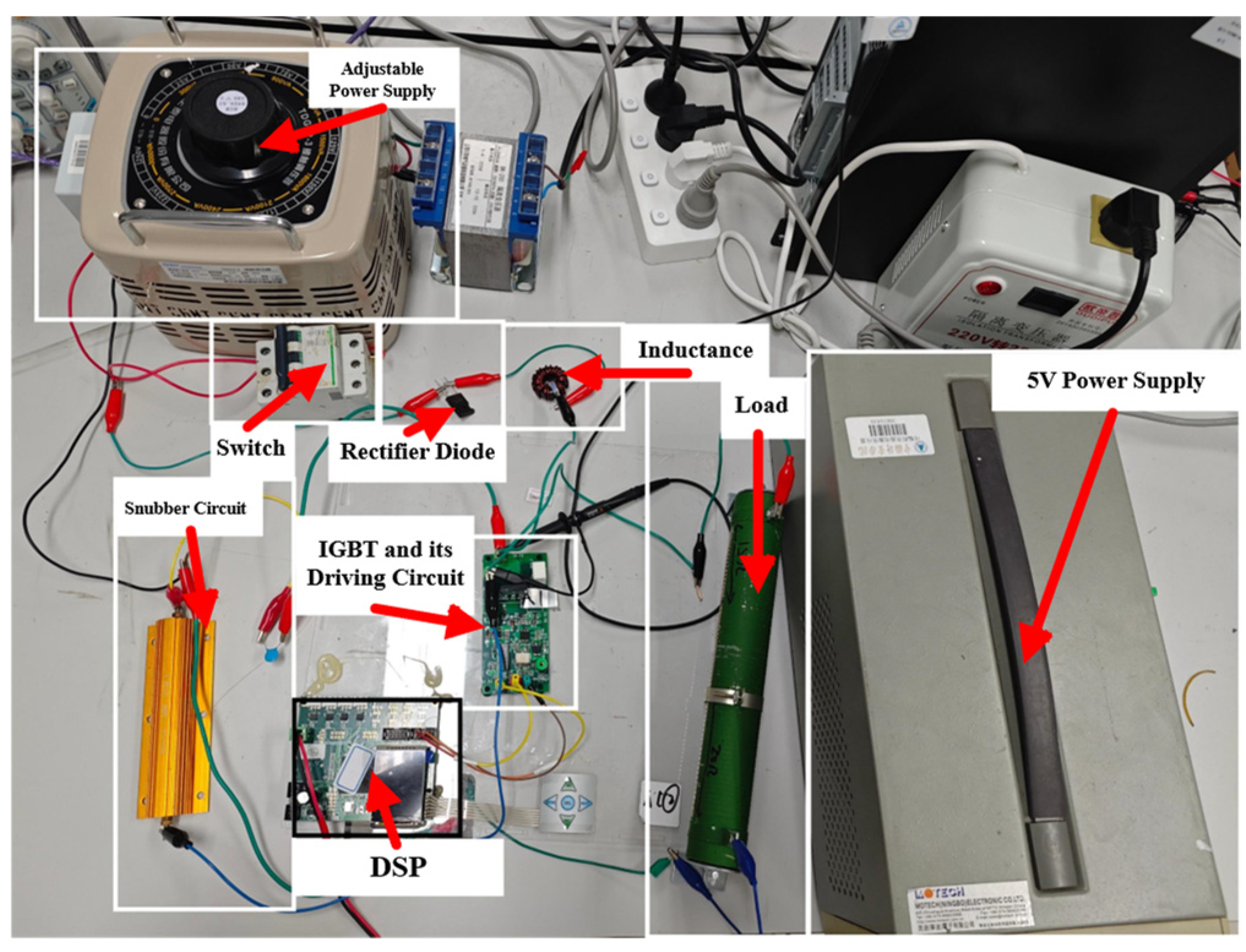
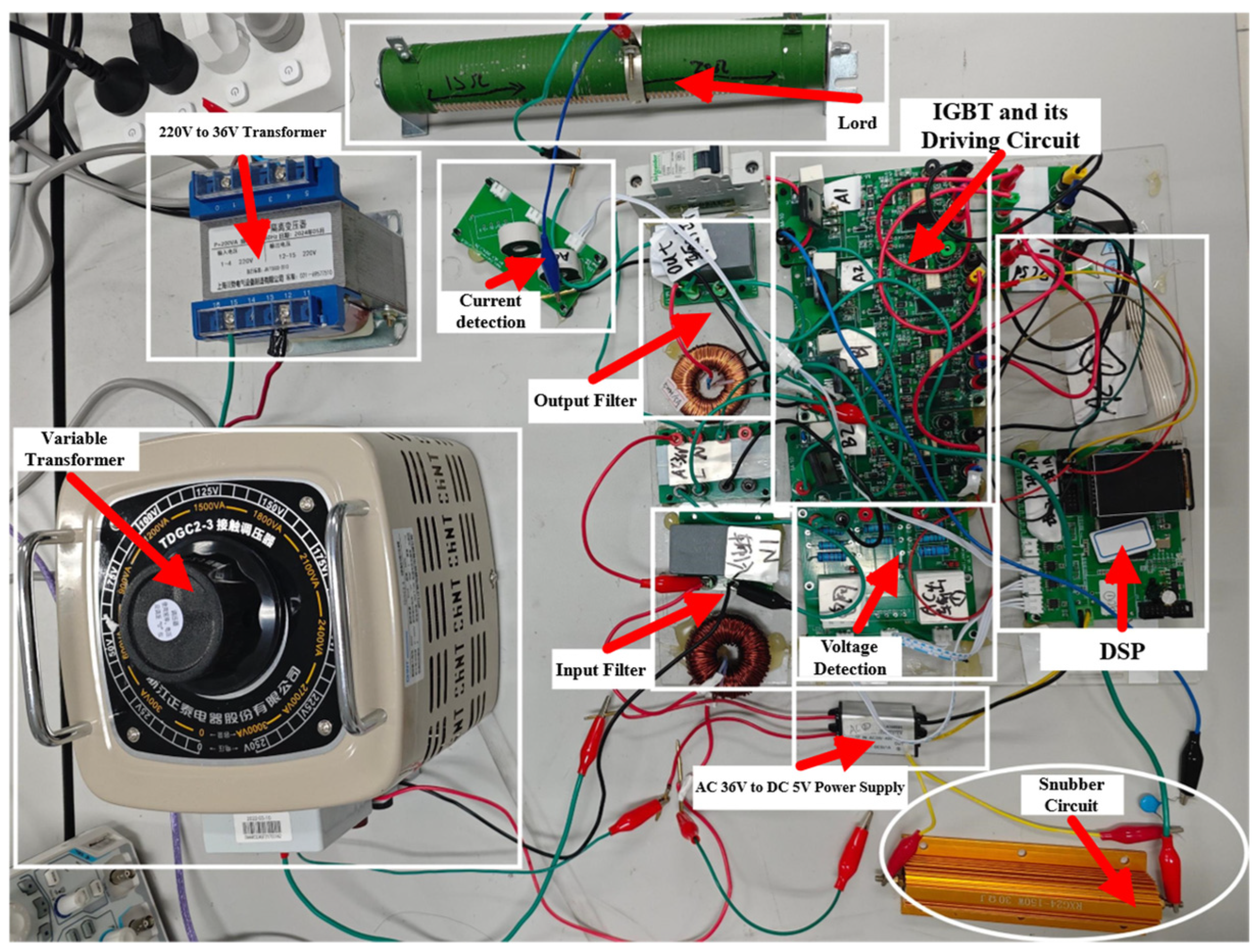
To test the optimized solution for the snubber circuit parameters, we constructed the circuit according to the topology in Figure 3. The experimental prototype, shown in Figure 7, includes the following components: an IGBT drive circuit, an IGBT power supply, an RC snubber circuit, a load resistor, a rectifier diode, and an inductance.
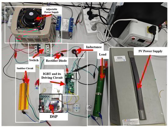
Figure 7.
Experimental prototype for verifying the optimization scheme of snubber circuit parameters.
Experiments were conducted using the following parameters: L = 400 μH, R = 20 Ω, input AC power with an effective value of 50 V, a fixed chopper duty cycle of 50%, and a switching frequency of 20 kHz. The IGBT model used is GT60M303, with a drop time of .
In reference [30], the empirical formula for the RC snubber circuit in AC–AC chopper converters is given as follows:
Substituting the circuit component parameters into Equation (24) for calculation gives the following parameter values for the RC snubber circuit:
The circuit component parameters are substituted into Equation (19) to derive the parameters of the AC–AC chopper converter RC snubber circuit according to the parameter optimization method of the AC–AC chopper converter proposed in this paper:
The experimental waveform diagram is shown in Figure 8, Figure 9, Figure 10, Figure 11, Figure 12, Figure 13, Figure 14, Figure 15 and Figure 16.
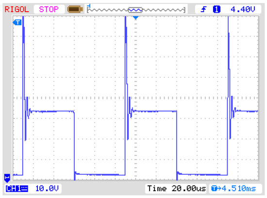
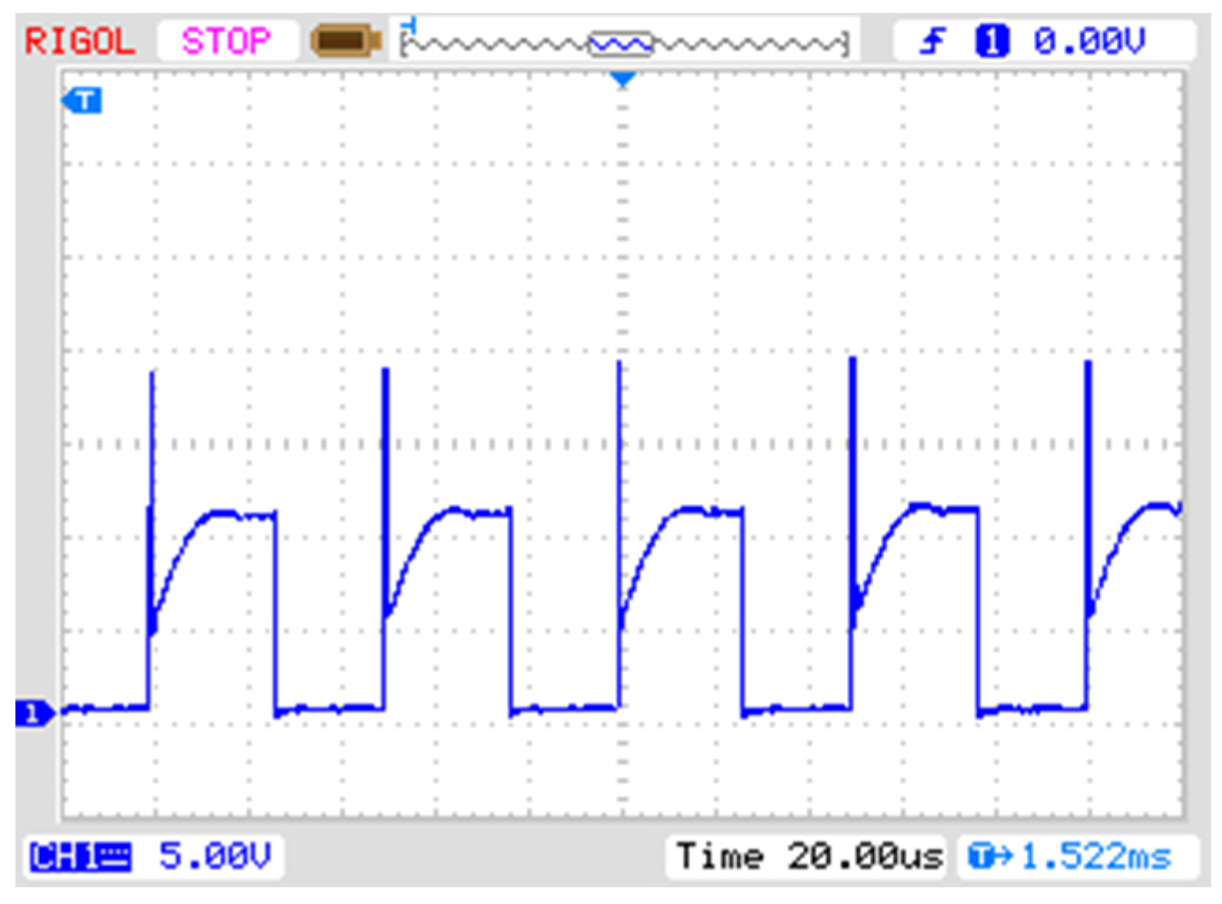
Figure 8.
with no snubber circuit.

Figure 9.
with , .

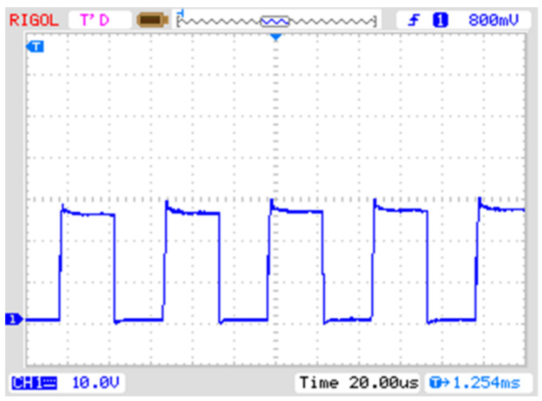
Figure 10.
with , .
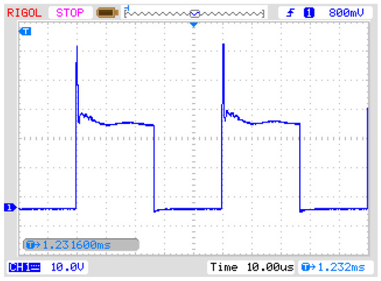
Figure 11.
with .

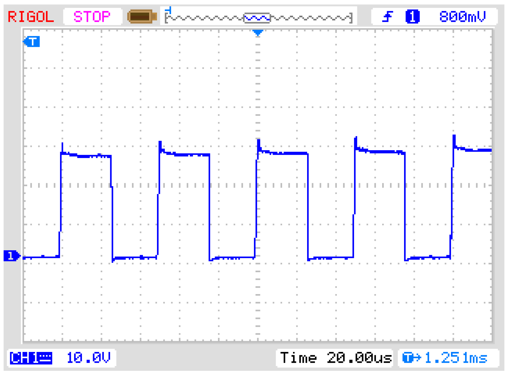
Figure 12.
with , .
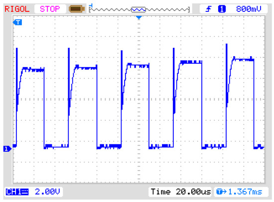
Figure 13.
with , .
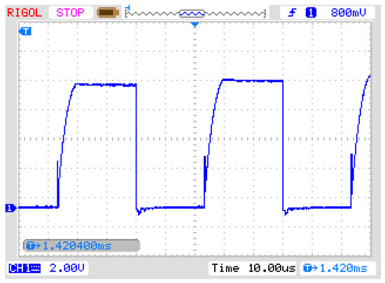
Figure 14.
with , .
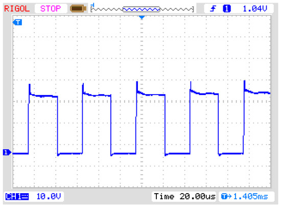
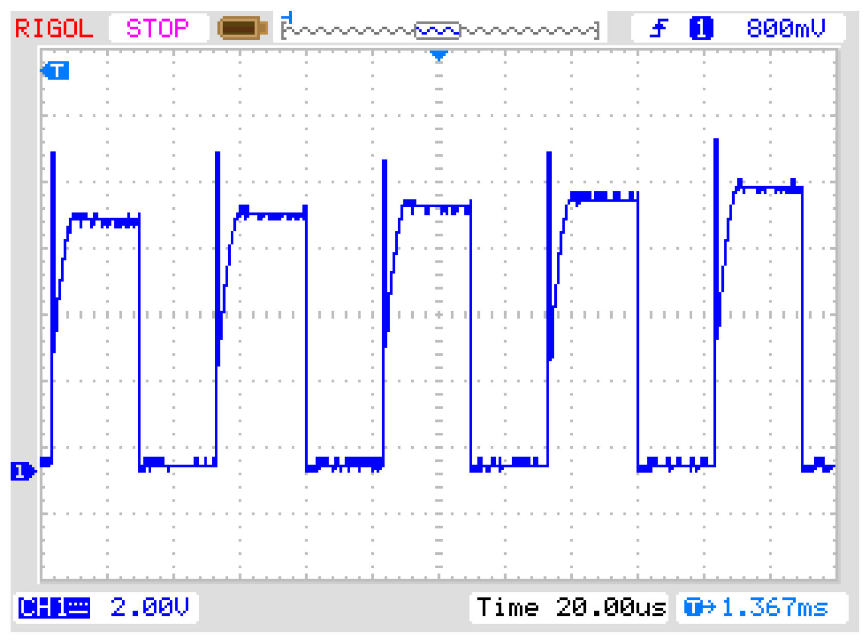
Figure 15.
with , .
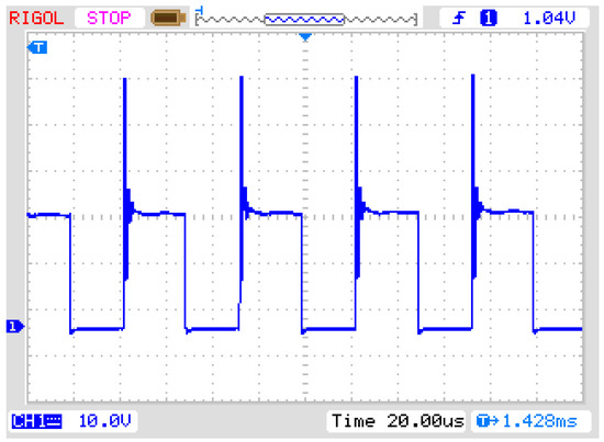
Figure 16.
with , .
In the initial experiment without a snubber circuit, significant voltage spikes were observed, with their waveform characteristics depicted in Figure 8. At this point the amplitude of the voltage spike reaches 243% of the reference voltage. Subsequently, experiments were conducted using parameters derived from the empirical formula for RC snubber circuits (Equation (25)), and the corresponding results are shown in Figure 9. The experimental waveforms indicate that, compared to the case without a snubber circuit, the spike amplitude decreased to 168% of the reference voltage. However, remained at a relatively high level, demonstrating that the conventional empirical formula-based parameter selection method for RC snubber circuits fails to effectively suppress voltage spikes.
When applying the RC parameter optimization method proposed in this paper to design the snubber circuit for the AC–AC chopper converter, the experimental results shown in Figure 10 reveal that, compared to Figure 8 and Figure 9, the waveform stabilized and the peak voltage was reduced to approximately the reference voltage level. This validates the effectiveness of Equation (23) in suppressing turn-off transient voltage spikes and demonstrates that the design achieves energy dissipation through proper matching of snubber resistor and capacitor parameters.
In order to study the influence of the snubber resistor value on the snubber circuit spike suppression, the snubber capacitance = 1 nF is kept unchanged in the experiment, and the snubber resistor is gradually increased to 200 Ω for the comparative test, and the corresponding results are shown in Figure 11.
The data show that when the value of is larger, the spike amplitude increases to 178% of the reference voltage, and the suppression effect of the snubber circuit is obviously weakened. This phenomenon is fully consistent with the theoretical prediction of Equation (12): when the snubber resistor exceeds the load resistor R, the impedance of the snubber circuit is too high, resulting in a delayed energy return. During circuit operation, the energy transfer between the snubber circuit and the load will be hindered, thus preventing the circuit from distributing and regulating the energy in a timely and efficient manner.
When maintaining = 1 nF constant and reducing to 5 Ω, the experimental waveform is shown in Figure 12. It can be observed from the figure that under this parameter selection, the peak voltage exhibits minimal variation, slightly exceeding the reference voltage. This is because reducing the resistance simultaneously decreases the time constant τ and shortens the discharge time. However, since the original τ was already sufficiently small and the discharge speed was adequately fast, further lowering the snubber resistor value does not enhance its performance. Conversely, this leads to severe issues, including power surges and overheating, capacitor breakdown due to excessive current, and high-frequency oscillations.
Subsequent investigations examined the impact of snubber capacitor selection on voltage spike suppression. When maintaining = 20 Ω constant and increasing to 22 nF, the experimental waveform shown in Figure 13 reveals that the peak voltage is reduced to 128% of the baseline voltage. Simultaneously, the waveform exhibits an overdamped response: following the switching action, the voltage experiences a brief undershoot, then gradually returns to the steady-state value through slow energy release from the capacitor, exhibiting a monotonic recovery characteristic without oscillations. This waveform behavior aligns with the theoretical mechanism described by Equation (18); increasing enhances the circuit’s energy storage capacity and prolongs the discharge process.
To further explore parameter synergy effects, the experiment tests the combined condition of = 22 nF and = 5 Ω, with waveforms shown in Figure 14. The results indicate that, due to the smaller τ value in this configuration, the system discharge rate accelerates, nearly eliminating the voltage spike . However, the larger snubber capacitance still induces overdamped behavior in the waveform.
Next, the discussion focuses on the case where the time constant :
When the snubber capacitance is extremely small, the experimental results shown in Figure 15 demonstrate that is significantly smaller than the value calculated using Equation (26). However, the experimental waveforms reveal no prominent voltage spikes or waveform distortion at , with the spike voltage controlled within 120% of the baseline voltage, which aligns with theoretical predictions.
However, when the snubber resistor is excessively large and fails to satisfy the condition in Equation (12), a distinct voltage spike at reaches 239% of the baseline voltage, as shown in Figure 16.
In order to quantify the impact of RC buffer circuit parameter matching on the system performance, the efficiency characteristics and overvoltage suppression effects under different − combinations are systematically compared, and the results are shown in Table 1. In this case, the device efficiency is obtained by Simulink numerical simulation (simulation step size 100 ns), while the overvoltage amplitude and percentage are derived from experimental waveform data.

Table 1.
Comparison table of the effect of RC buffer circuit parameter combinations on system efficiency and overvoltage rejection characteristics.
According to the experimental data in Table 1, the voltage spike amplitude exhibits a negative correlation with system efficiency. When the peak voltage is suppressed within 10% of the reference voltage, the system conversion efficiency can exceed 92%. Conversely, if the RC snubber circuit parameters are mismatched, it not only induces transient overvoltage across the power switching devices but also results in efficiency losses up to 55%. This is attributed to exacerbated Ohmic losses in the snubber resistor and insufficient energy feedback during the switching process.
The experimental prototype is illustrated in Figure 17. It employs the digital signal processing (DSP) chip of TMS320F28335 as the control core to generate an experimental prototype of the alternating current-alternating current converter. Input is AC voltage with a valid value of 50V.

Figure 17.
Experimental prototype of the AC–AC chopper converter.
The experimental prototype utilizes a sampling module to determine the polarity of the input voltage and load current. The conduction and turn-off states of the IGBTs are managed based on the control timing diagram shown in Figure 6 and the duty cycle signals provided by the control chip. The input AC voltage is chopped, filtered, and then delivered to the load, with closed-loop control implemented through voltage sampling for load voltage monitoring.
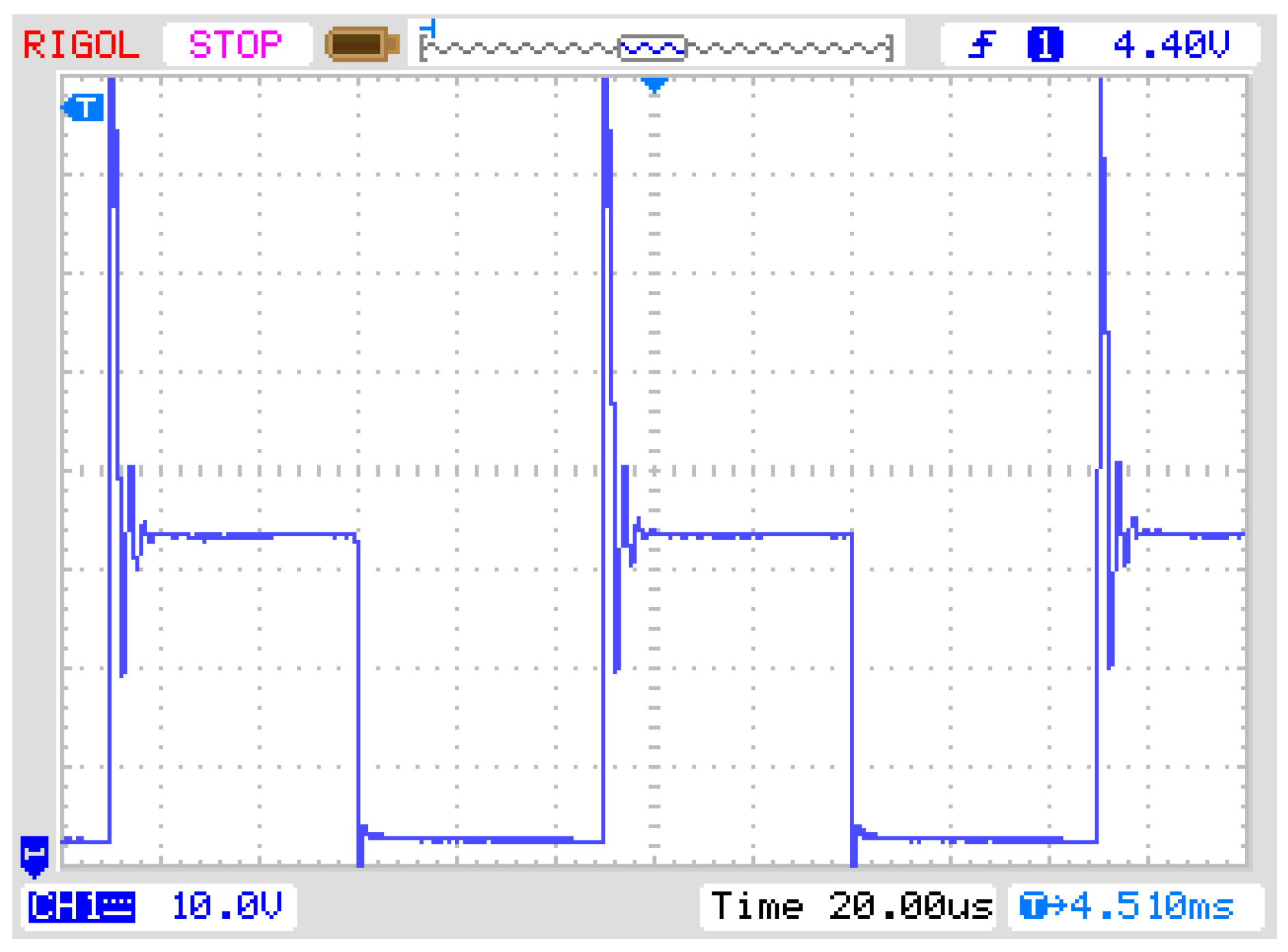
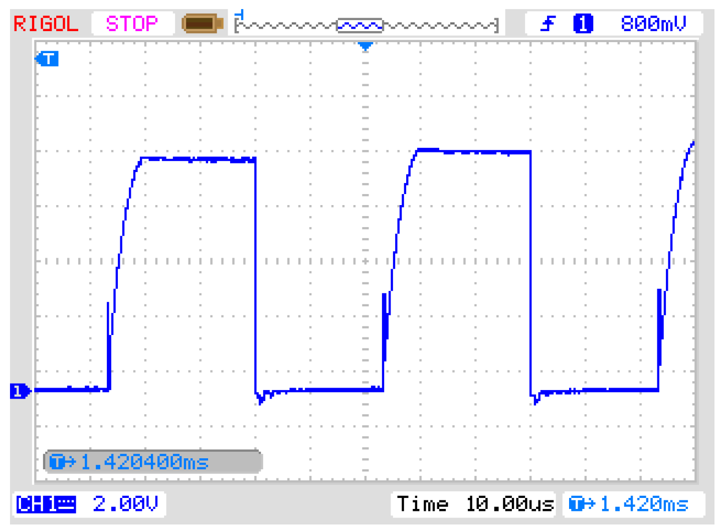
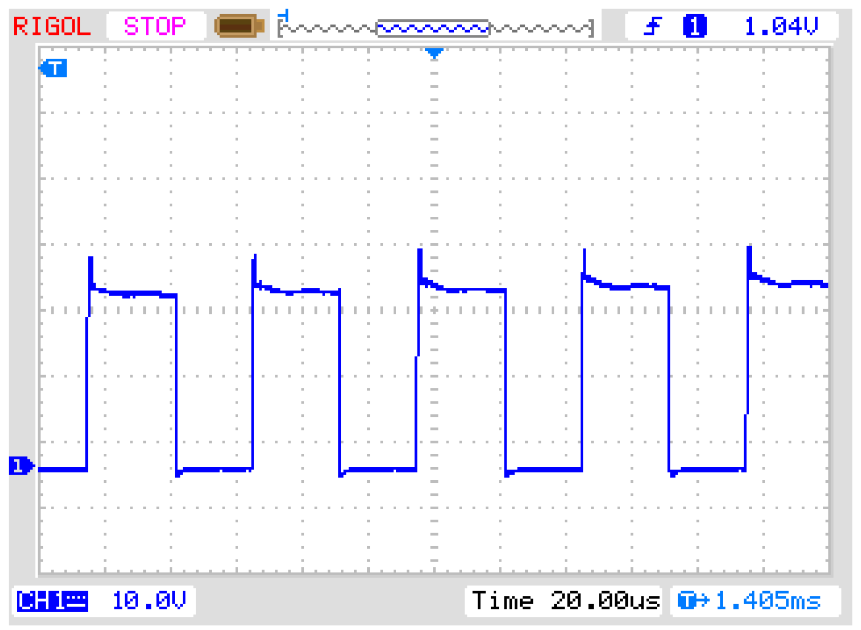
When the reference voltage RMS value is set to 50 V, the prototype achieves voltage control within the 0 to 48 V RMS range. The waveform at a target output voltage amplitude of 36 V is shown in Figure 18. Simultaneously, when the load resistance decreases from 20 Ω to 12 Ω, the load current transient waveform is illustrated in Figure 19.
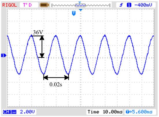
Figure 18.
The reference voltage is 36 V.
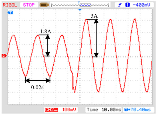
Figure 19.
The current when the reference voltage is 36 V and the load jumps from 20 Ω to 12 Ω.
6. Conclusions
The application significance and current research status of AC–AC chopper converters are first introduced in this paper, and their detailed working principles are analyzed. It then explains the causes of voltage spikes in the circuit and their suppression methods, presenting parameter calculation formulas for the RC snubber circuit in AC–AC chopper converters. Subsequently, the system control timing is analyzed under different load conditions, and a small-signal model of the AC–AC chopper converter with a snubber circuit is proposed. A control diagram for the system is presented, along with a stability analysis. Based on the derived theory, experiments demonstrate the feasibility of the new calculation formula for the improved RC snubber circuit. The experimental prototype achieves voltage regulation functionality for the AC–AC chopper converter.
Author Contributions
Conceptualization, L.W.; Methodology, J.H.; Software, G.L.; Theoretical guidance, C.S.; Writing—original draft, Z.S.; Writing—review & editing, Z.S. All authors have read and agreed to the published version of the manuscript.
Funding
This work was supported by the Natural Science Foundation of Zhejiang Province under Grant LY22E070008, Zhejiang colleges and universities leading talent training plan, and Yiwu City Natural Science Research Project.
Data Availability Statement
The original contributions presented in this study are included in the article. Further inquiries can be directed to the corresponding author.
Conflicts of Interest
Author declares no conflict of interest.
References
- ReferencesPatin, N. 4-AC/AC Converters. In Power Electronics Applied to Industrial Systems and Transports, Volume 2; Patin, N., Ed.; Elsevier: Amsterdam, The Netherlands, 2015; pp. 161–191. [Google Scholar]
- Szcześniak, P.; Kaniewski, J.; Jarnut, M. AC–AC power electronic converters without DC energy storage: A review. Energy Convers. Manag. 2015, 92, 483–497. [Google Scholar] [CrossRef]
- Gambôa, P.; Silva, J.F.; Pinto, S.F.; Margato, E. Input–Output Linearization and PI controllers for AC–AC matrix converter based Dynamic Voltage Restorers with Flywheel Energy Storage: A comparison. Electr. Power Syst. Res. 2019, 169, 214–228. [Google Scholar] [CrossRef]
- Bulut, E.B.; Gulbahce, M.O.; Kocabas, D.A. Analysis of a GaN based PWM AC-AC chopper converter with an improved switch loss model. AEU-Int. J. Electron. Commun. 2021, 131, 153578. [Google Scholar] [CrossRef]
- Munoz-Hernandez, G.E.A. Evaluating a Scheduling Fractional-Order Controller in an AC/AC Matrix Converter Driving a PMSM Model. IFAC-Pap. 2024, 58, 344–349. [Google Scholar] [CrossRef]
- Jamna, A.; Pradeep, J.; Jamuna, V. Comparative analysis of voltage controllers for a single stage AC-AC chopper converter for Aircraft Ground power unit application. Mater. Today Proc. 2021, 45, 2381–2390. [Google Scholar]
- Hovorov, P.; Khvorost, M.; Kindinova, A.; Abdelrhim, O. Voltage regulation in electrical networks using booster transformers with thyristor control. In Proceedings of the 2023 IEEE 4th KhPI Week on Advanced Technology (KhPIWeek), Kharkiv, Ukraine, 2–6 October 2023; pp. 1–5. [Google Scholar]
- ESosnina; Anatoliy, A.; Bedretdinov, R.; Kryukov, E.; Gusev, D. The Claimed Functions of A Thyristor Voltage and Power Regulator Research. In Proceedings of the 2023 IEEE International Smart Cities Conference (ISC2), Bucharest, Romania, 24–27 September 2023; pp. 1–4. [Google Scholar]
- Chen, X.Y.; Luo, H.Y.; Li, L.Y.; Qian, H.H.; Yang, Y.Y.; Ran, X.Y.; Guo, C. Design and Digital Control of a Cryogenic Boost-Buck Chopper. In Proceedings of the 2015 IEEE International Conference on Applied Superconductivity and Electromagnetic Devices (ASEMD), Proceedings Paper, Shanghai, China, 20–23 November 2015; pp. 15–16. [Google Scholar]
- Xu, B.; Gao, C.; Zhang, J.; Yang, J.; Xia, B.; He, Z. A Novel DC Chopper Topology for VSC-Based Offshore Wind Farm Connection. IEEE Trans. Power Electron. 2021, 36, 3017–3027. [Google Scholar] [CrossRef]
- Li, P.; Zhang, L.; Ouyang, B.; Zhai, X. Research on Ground Current of High-Power Series Chopper Circuit. In Proceedings of the 2018 4th International Conference on Environmental Science and Material Application, Proceedings Paper, Xi’an, China, 15–16 December 2019; Volume 252. [Google Scholar]
- Zhang, Z. Research on the Development Prospect of DC Chopper Convertor. In Advances in Materials, Machinery, Electronics Iii; Proceedings Paper; AIP Publishing: Melville, NY, USA, 2019; Volume 2073. [Google Scholar]
- Yu, J.; Xia, C. Operation and control schemes of a novel direct AC-AC modular multilevel converter. Int. J. Electr. Power Energy Syst. 2022, 139, 108037. [Google Scholar] [CrossRef]
- Liu, C.; Guo, D.; Shan, R.; Cai, G.; Ge, W.; Huang, Z.; Wang, Y.; Zhang, H.; Wang, P. Novel Bipolar-Type Direct AC-AC chopper converter Topology Based on Non-Differential AC Choppers. IEEE Trans. Power Electron. 2019, 34, 9585–9599. [Google Scholar] [CrossRef]
- Hu, Y.; Jiang, L.; Wen, W.; Yan, W.; Ding, R. A New Adaptive Drive Voltage Approach for LED Driver. In Proceedings of the 2019 IEEE Applied Power Electronics Conference and Exposition (APEC), Anaheim, CA, USA, 17–21 March 2019. [Google Scholar]
- Bhardwaj, S.R.; Rahi, O.P.; Sharma, V. Comparative Analysis of Induction Motor Drive with Chopper Controlled SPRS Employing Various Inverter Configurations. IETE J. Res. 2019, 65, 329–341. [Google Scholar] [CrossRef]
- Summatta, C.; Sanmuang, S.; Prainatr, S. Improvement of Asymmetrical Pulse Width Modulation Switching Function for AC Chopper. In Proceedings of the 2018 15th International Conference on Electrical Engineering/Electronics, Computer, Telecommunications and Information Technology (Ecti-Con), Proceedings Paper, Chiang Rai, Thailand, 18–21 July 2018; pp. 441–444. [Google Scholar]
- Zhao, F.; Li, Y.; Tang, Q.; Wang, L. Analysis of oscillation in bridge structure based on GaN devices and ferrite bead suppression method. In Proceedings of the 2017 IEEE Energy Conversion Congress and Exposition (ECCE), Cincinnati, OH, USA, 1–5 October 2017; pp. 391–398. [Google Scholar]
- Yang, X.; Xu, M.; Li, Q.; Wang, Z.; He, M. Analytical Method for RC Snubber Optimization Design to Eliminate Switching Oscillations of SiC MOSFET. IEEE Trans. Power Electron. 2022, 37, 4672–4684. [Google Scholar] [CrossRef]
- Che, L.; Dong, Y.; Lei, G. Design Optimization of RC Snubber Circuit for A SiC Power Module. In Proceedings of the 2022 23rd International Conference on Electronic Packaging Technology (ICEPT), Dalian, China, 10–13 August 2022; pp. 1–6. [Google Scholar]
- Ahmad, H.J.; Hagiwara, M. Interleaved Bidirectional Chopper with Auxiliary Converters for DC Electric Railways. IEEE Trans. Power Electron. 2021, 36, 5336–5347. [Google Scholar] [CrossRef]
- Ding, Y.; Mao, S.; Liu, H.; Tan, Q.; Yang, S.; Liu, P. Modeling of SiC MOSFETs Switching Oscillation for Dynamic Optimization with RC Snubber in the Half-bridge Circuit. In Proceedings of the 2023 IEEE Energy Conversion Congress and Exposition (ECCE), Nashville, Tennessee, 29 October–2 November 2023; pp. 5970–5975. [Google Scholar]
- Du, H.; Wu, J.; Meng, F. Research on the Formation Principle and Suppression Method of Switch Spike Voltage in Reverse LLC Resonant Converter. In Proceedings of the 2022 Asia Power and Electrical Technology Conference (APET), Shanghai, China, 11–13 November 2022; pp. 127–131. [Google Scholar]
- Feng, Y.; Chen, X.; Song, M.X.; Zhang, T. High-power IGBT Overvoltage Spike SuppressionBased on Gate Voltage Modulation. Appl. Sci. 2021, 55, 137–140. [Google Scholar]
- Yang, J.; Shan, R.; Huang, S. A Novel Bipolar Direct PWM Controlled Buck-Type AC/AC Converter. In Proceedings of the 2023 5th International Conference on Electronic Engineering and Informatics (EEI), Wuhan, China, 23–25 June 2023; pp. 93–98. [Google Scholar]
- Elias, N.; Azmi, S.A.; Zaidi, A.F.A.; Tajuddin, M.F.N.; Rahim, S.R.A. Performance Evaluation of DC-DC Buck Converter with RC Snubber Circuit Under Ideal and Non-Ideal Conditions. In Proceedings of the 2024 4th International Conference on Electronic and Electrical Engineering and Intelligent System (ICE3IS), Yogyakarta, Indonesia, 4–5 November 2024; pp. 225–230. [Google Scholar]
- Pradipta, D.; Hasanah, R.N.; Nurwati, T. Active Gate Driver with RC Snubber and Proportional-Integral (PI) Controller for Voltage Balancing of Series Connected SiC MOSFETs. In Proceedings of the 2024 4th International Conference of Science and Information Technology in Smart Administration (ICSINTESA), Balikpapan, Indonesia, 12–13 July 2024; pp. 622–627. [Google Scholar]
- Tuncay, S.; Zeng, G.; Si, G.; Basler, T. SiC Trench MOSFETs in Avalanche Mode with RC Snubber Circuit. In Proceedings of the PCIM Europe 2024; International Exhibition and Conference for Power Electronics, Intelligent Motion, Renewable Energy and Energy Management, Nuremberg, Germany, 11–13 June 2024; pp. 1853–1859. [Google Scholar]
- Zhang, B.; Han, W.; Cao, B.; Hu, W.; Hu, Y. Optimum Design of Wireless Power Transfer-Based Snubbers for SiC MOSFET Switching Oscillations. IEEE Trans. Power Electron. 2024, 39, 10710–10715. [Google Scholar] [CrossRef]
- Ahmed, H.F.; Chung, C.H.; Khan, A.A.; Aleem, Z.; Akbar, F.; Alzaabi, O. Nondifferential AC Choppers Based Identical Bipolar Buck–Boost AC–AC Converter Without Commutation Issue. IEEE Trans. Power Electron. 2023, 38, 4988–4999. [Google Scholar] [CrossRef]


Disclaimer/Publisher’s Note: The statements, opinions and data contained in all publications are solely those of the individual author(s) and contributor(s) and not of MDPI and/or the editor(s). MDPI and/or the editor(s) disclaim responsibility for any injury to people or property resulting from any ideas, methods, instructions or products referred to in the content. |
© 2025 by the authors. Licensee MDPI, Basel, Switzerland. This article is an open access article distributed under the terms and conditions of the Creative Commons Attribution (CC BY) license (https://creativecommons.org/licenses/by/4.0/).