Article

Application of Highly Spatially Resolved Area Array Velocity Measurement in the Cracking Behavior of Materials

Key Laboratory of Shock Wave and Detonation Physics, Institute of Fluid Physics, China Academy of Engineering Physics, Mianyang 621900, China
*
Author to whom correspondence should be addressed.
Electronics 2025, 14(9), 1732; https://doi.org/10.3390/electronics14091732
Submission received: 27 February 2025 / Revised: 21 April 2025 / Accepted: 22 April 2025 / Published: 24 April 2025
(This article belongs to the Special Issue Advanced Optoelectronic Sensing Technology)

Abstract

:
Understanding microscale dynamic behavior in heterogeneous materials (e.g., polycrystalline or semiconductor systems) under impact loading requires diagnostics capable of resolving ~100 μm features. This study introduces a 19-core fiber-optic array probe with 100 μm spatial resolution, integrated with DISAR velocimetry on a light gas gun platform, enabling two-dimensional continuous measurement of free-surface velocity. The system overcomes limitations of conventional single-point methods (e.g., VISAR’s millimeter-scale resolution and reflectivity constraints) by achieving nanosecond temporal resolution and sub-nanometer displacement sensitivity. Under ~8 GPa impact loading, the probe captures spatiotemporal velocity heterogeneity in polycrystalline materials, including localized pull-back signals and periodic oscillations caused by shock wave reflections at microstructural interfaces. These observations reveal dynamic processes such as damage initiation and evolution, directly linking velocity profiles to microscale material response. The results provide experimental evidence of how grain-scale defects influence shock propagation and energy dissipation, advancing predictive models for extreme-condition material performance. This high-resolution, multi-channel approach offers a paradigm shift in diagnosing heterogeneous material behavior under high-strain-rate loading.

1. Introduction

Given their role as core materials of modern electronic devices and solar cells, the study of semiconductor materials under shock loading is of great significance to improve their reliability and performance. As a typical semiconductor material, the dynamic deformation and fracture behavior of monocrystalline silicon under impact loading have been widely studied [1]. The results show that there are significant differences in the volume stress history and fracture mode of monocrystalline silicon when it is loaded in different directions relative to its crystal structure. For example, in the split Hopkinson pressure bar experiment, with in-situ X-ray imaging and diffraction systems, the volume stress history can be measured and the Lowe diffraction pattern can be observed, revealing microstructural changes in the material under impact loading [2]. Semiconductor materials are susceptible to cracks and voids under impact loading, especially under thermal shock conditions [3]. In laminar cracking experiments on copper, PDV (Photonic Doppler Velocimetry) identified the critical strain threshold of hole nucleation through μs velocity fluctuations (Δv ~10 m/s), which was consistent with the damage distribution shown on SEM (Scanning Electron Microscopy) images [4].
Due to the average effect of single-point velocity measurement in the spatio-temporal domain, the two-dimensional shock wave velocity field cannot be truly and comprehensively reflected [5]. Research progress into high spatially resolved area array velocity measurement technology in the field of shock waves mainly focuses on the use of area array CCD and CMOS image sensors for high-precision velocity measurement [6,7,8]. These technologies combine narrow-band filters, spatial filtering techniques, and differential detection techniques to accurately measure the velocity and displacement of moving targets [9]. The application of area array CCD and CMOS image sensors in velocity measurement has been widely studied [10]. For example, spatial filtering velocimetry technology of an area array CCD has been used to measure the velocity field distribution of particle flow, and the spatial filtering characteristics of multi-slit systems are simulated by interlaced sampling, so as to realize the optical non-contact measurement of particle velocity in obstacle flow. In addition, spatial filter velocimetry (SFV) of the area array CCD does not need to track tracer particles, and only requires an ordinary LED light source, showing strong environmental adaptability and ease of operation [11,12,13].
In addition to area array CCD spatial filtering technology, laser interferometric velocimetry is also an important tool in shock wave physics research. Laser interferometers use the Doppler effect to measure the velocity of shock waves, which is characterized by high accuracy. For example, velocity interferometers (VISARs) on arbitrary reflective surfaces are commonly used to measure free-surface velocities, interface velocities, and particle velocities, among other things [14,15,16]. These measurements are of great significance for deriving the stress–strain state of materials and establishing a theoretical model of the state of matter. VISAR (Velocity Interferometer System for Any Reflector) requires highly reflective surfaces with high requirements for surface flatness and normal incidence, which is susceptible to noise interference, and requires complex optical setups and synchronized streak cameras [17]. DISAR (Displacement interferometer system for any reflector) is prone to introduce noise because it uses two signals to calculate the displacement and then differentially derive the velocity [5].
The study of the behavior of semiconductor materials under impact loading is a complex and diverse field, involving many aspects such as dynamic deformation, plastic behavior, damage modes, and anisotropic responses [18,19,20]. Through experiments and numerical simulation methods, the response mechanism of these materials under extreme conditions can be deeply understood, so as to provide a scientific basis for the design and optimization of semiconductor devices. Future research will further reveal the microscopic mechanisms of semiconductor materials under impact loading [21,22,23]. Area array probes capture the difference in shock wave velocity in different regions, revealing the preferred onset location of material damage in the spatial dimension. In the time dimension, the nanosecond dynamic process of shock wave propagation can be resolved. Shock-induced velocity heterogeneity, surface roughening, and micro-ejection in heterogeneous materials present critical challenges for optical free-surface velocity measurements.
In this paper, a highly spatially resolved velocity measurement technique is used to obtain the dynamic response behavior of materials under impact loading (~8 GPa). Firstly, the spatial area measurement point distribution is realized by using the area array fiber close-row method and the coupling of optical lens groups. Secondly, combined with the high-precision and continuous measurement characteristics of laser interferometry velocimetry, a highly spatially resolved area array velocity measurement technology is formed. Last, the mechanism of material inhomogeneity or anisotropy under impact loading is experimentally studied.

2. Materials and Methods

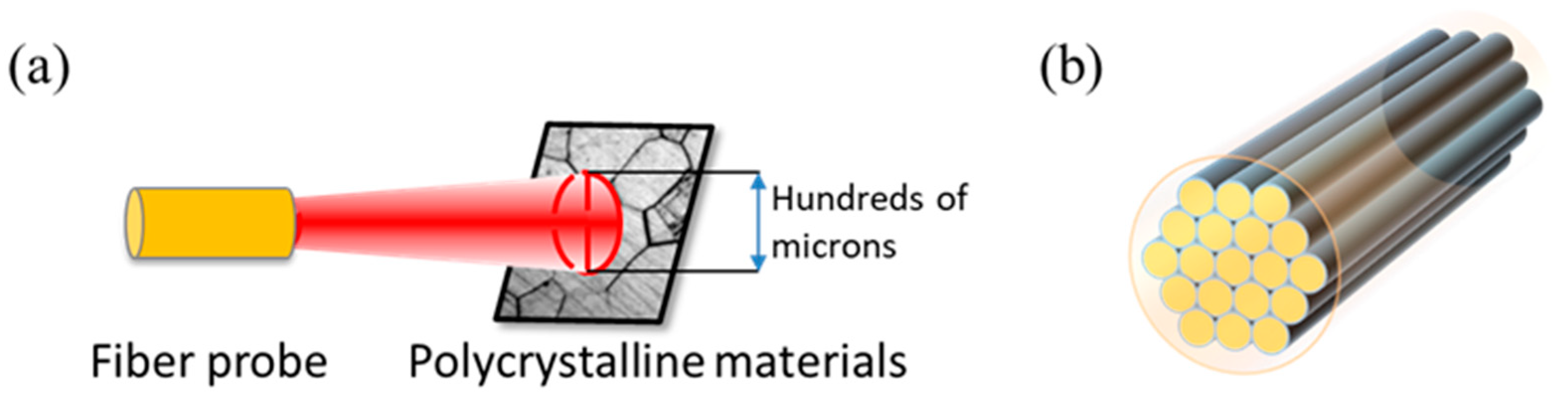
2.1. Area Array Fiber Optic Probes

The spatial resolution of traditional velocimetry techniques (e.g., single-point VISAR or electric probe) is often in the millimeter range (e.g., millimeter-level spacing of early and mid-to-middle VISARs), making it difficult to resolve the dynamic response of grain boundaries, holes, or phase interfaces. Technology with 100 μm resolution captures the following details: (1) Microporous nucleation and expansion: In the explosive impact initiation experiment, the velocity fluctuation and micropore distribution corresponding to the critical strain of hole nucleation can be identified with a resolution of 100 μm. (2) Grain boundary slip and shear band formation: The impact experiment on the high-entropy alloy CoCrNi shows that the velocity gradient in the grain boundary region (Δv/Δx ≈ 200 m/s/mm) can only be quantitatively analyzed at 100 μm resolution, revealing the preferential damage mechanism of grain boundaries [24].
DISAR (the manufacturer is Institute of Fluid Physics, China) and VISAR (the manufacturer is Sandia National Laboratories, America) are the two dominant velocity measurement techniques in impact dynamics, with DISAR offering superior stability (30% + improvement) and precision (50 ps response time) by eliminating free-space optical errors through fiber-based Doppler demodulation, as shown in Table 1.
Based on a fiber close-row array and optical lens, a laser transmitting and receiving integrated probe with spatial resolution is designed. The goal is a multi-point measurement system with a large stroke, and to improve the depth of field of the optical system, it is necessary to design a telecentric optical path structure with a small object numerical aperture. Single-mode fiber close-row array and optical lens group coupling technology is adopted. As shown in Figure 1a, the emitted spot of a single fiber probe is typically around 200 μm. When a material exhibits inhomogeneities such as polycrystallinity or cracks, the entire spot area covers the differences caused by these inhomogeneities. This averages out these differences, and the final measured speed is an average. To improve the spatial resolution to measure the differences due to non-uniformity, multiple fibers were geometrically closely arranged to obtain an area array bundle, as shown in Figure 1b.
According to the principle of geometrical optics and measurement requirements, an optical lens is designed to be coupled with the fiber bundle, as shown in Figure 2b. A 19-core fiber bundle was selected, with a total of two turns except for one fiber in the center. To obtain a long working distance and a large depth of field, the selected optical lenses were parametrically optimized using ZEMAX software version 2024 R2.02. Figure 2a shows, from left to right, the fiber bundle, the lens, and the surface being measured. After optimization, the lens has a thickness of 2.05 mm and a diameter of 0.636 mm. It is an aspherical lens with a focal length of 5 mm. The actual probe obtained is shown in Figure 2c.
The imaging effect can be seen from the point spread function (PSF) diagram; that is, the spot of the central fiber is optimal, and the spot far from the optical axis is distorted, as shown in Figure 3a. The “OBJ” and “IMA” in the point diffusion diagram represent the object plane and the image plane, respectively. In addition, it is possible to see the image quality of the imaging system in different fields of view, such as the difference in imaging between the off-axis field of view and the defocus plane. As shown in Figure 3b, the spot is more rounded in the focal plane and on the optical axis. Off-axis spot aberrations are the largest, which also limits the number of area array fibers. The out-of-focus spot appears to be smaller and smaller in the direction of the light source, and conversely the spot becomes larger with increasing distance from the light source. This means that when measuring, the user must not move away from the length of the focal point.
The design balances spatial resolution (120 µm) and field of view (1.5 mm diameter) through a 19-core fiber array, maintaining telecentricity without complex multi-lens corrections. Pre-experiment point-spread-function (PSF) mapping (Figure 3 and Figure 4) quantifies residual optical aberrations, enabling software-based intensity normalization and positional corrections. Real-time pulse delay adjustments, guided by ZEMAX-predicted optical path differences, synchronize all 19 channels to <50 ps timing jitter. Together, these measures ensure <5% velocity error at peripheral measurement points despite off-axis distortion, resolving critical 100 µm-scale material heterogeneities (grain–boundary slip, microvoid nucleation) under shock loading. This systematic approach guarantees fidelity across the measurement field while addressing inherent tradeoffs in high-resolution dynamic diagnostics.
The focal spot size and spacing of the 19-core area array fiber optic probe were measured under an optical microscope as shown in Figure 4a. The focal spot diameter is approximately 20 μm, and the distance between adjacent spots is about 120 μm. This also illustrates that the spatial resolution of the measurement point is about 120 μm. The spot size and energy distribution were observed under a spot analyzer, as shown in Figure 4b. The overall spot size is relatively uniform, and the energy difference between the channels is small.

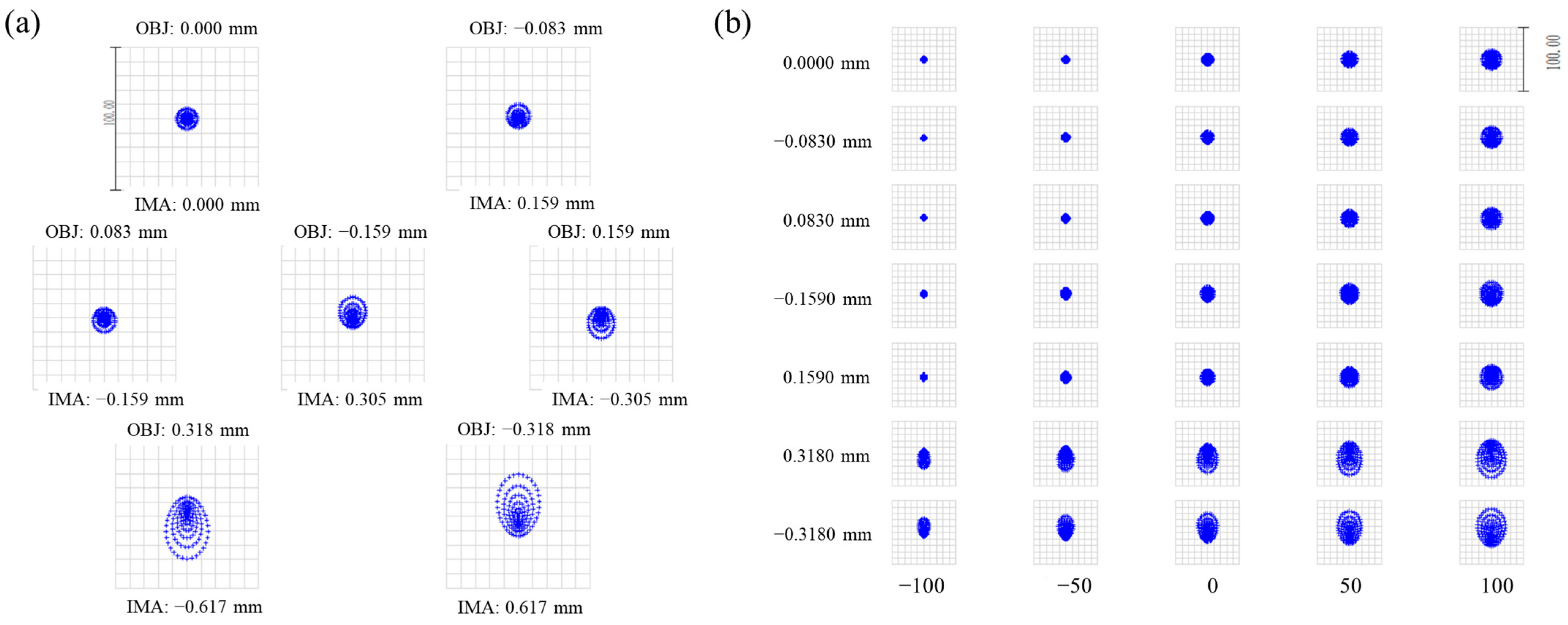
2.2. Experimental System

Free surface velocity is a key parameter in impact dynamics, reflecting multi-physics coupling processes like stress wave propagation, damage evolution, and phase transitions. Grain boundaries critically influence its spatiotemporal evolution—lower grain boundary density in large-grained materials reduces rebound amplitude, indicating a higher damage initiation threshold, while grain orientation differences cause local stress wave velocity non-uniformity.
The light gas gun is a key laboratory tool for studying high-strain-rate dynamic responses, enabling controlled shock wave loading (108–1011 Pa, μs duration) with precise pressure and duration adjustment via gas pressure, projectile mass, and target material. Its strain rate range (105–106 s−1) facilitates analysis of critical dynamic processes, including elastoplastic transition, phase transformation, and fracture damage, while high spatiotemporal diagnostics reveal wave–wave and wave–defect interactions. The experimental test system is divided into a DISAR velocimeter, an oscilloscope and an area array fiber optic probe as shown in Figure 5a. The experimental design drives the metal projectile to hit the non-uniform target material at high speed on the light gas gun loading platform, as shown in Figure 5b. The center spot of the area array probe is aligned with the center of the non-uniform target, while the projectile is aligned with the target through the guide pipe. The target material to be tested is a disc with a diameter of 10 mm and a thickness of 2 mm. The velocity of the projectile is 428 m/s, which is determined by the pressure of the compressed helium. Since the area array probe has 19 cores, the DISAR velocimeter corresponds to 19 channels. To avoid crosstalk of adjacent signals, the wavelengths of the four fibers next to each other are set differently. The inhomogeneous target material is polycrystalline, with a grain size of about 100 μm, which is just in line with the spatial resolution of the probe. Because laser velocity measurement requires that the measured surface can reflect enough intensity of signal light into the probe, the single-point exit light power of the probe should not be less than 50 mW, and the roughness of the measured surface should not be less than the laser wavelength (i.e., 1.5 μm).

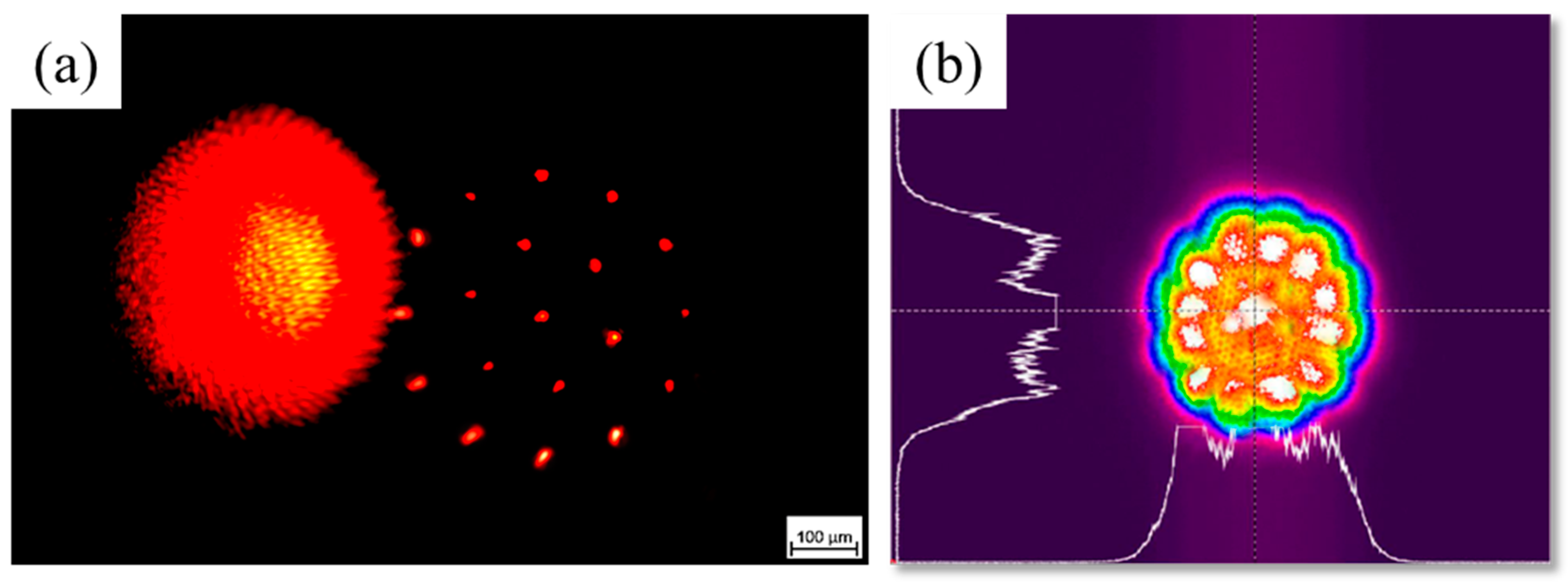
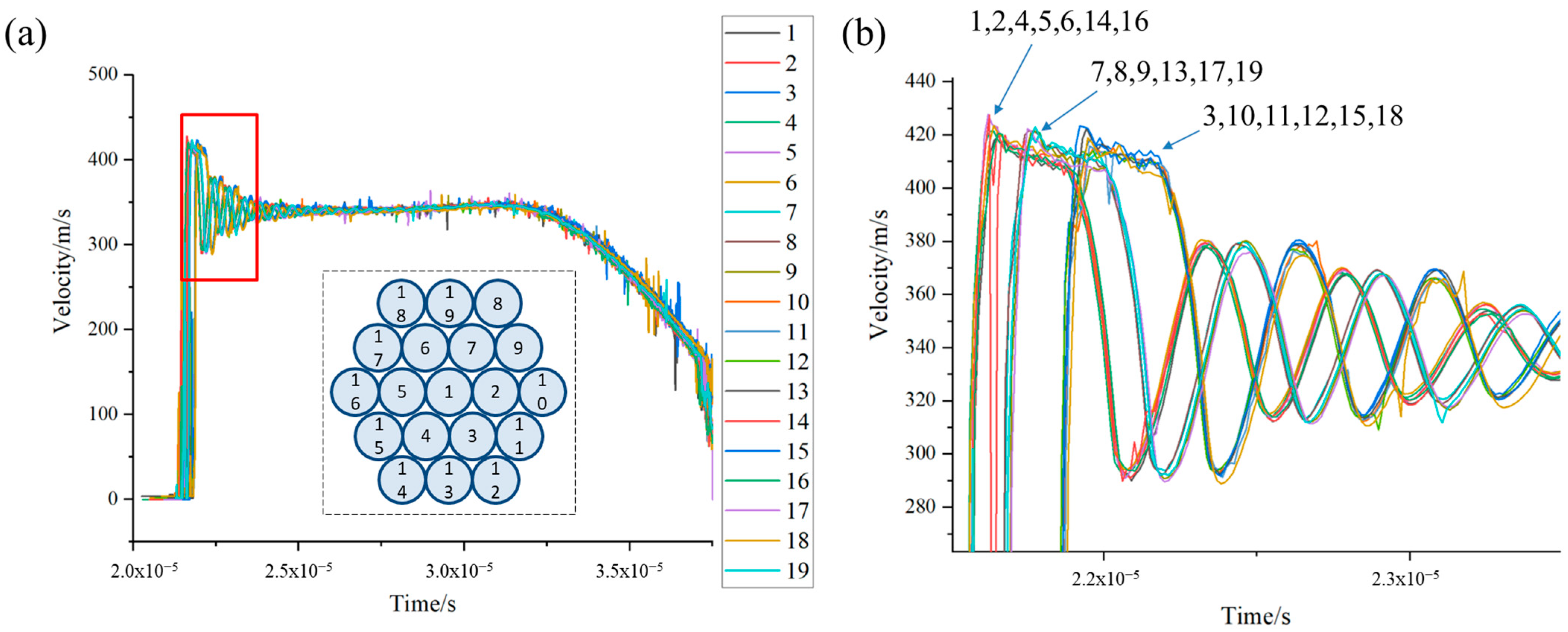
3. Results and Discussion

The free-surface velocity curve obtained by the shock wave was reflected many times in the inhomogeneous material, as shown in Figure 6a. The dotted box in Figure 6a shows the distribution of the measurement points of the 19-core area array fiber probe, which corresponds to the velocity curve of each measurement point. When the shock wave reaches the free surface of the target plate, the free surface velocity suddenly increases and reaches a loading plateau value (~420 m/s), which is due to the direct action of the shock wave. Subsequently, when the right-hand sparse wave head reflected from the free plane behind the flyer crosses the target plate to the free surface of the target plate, the free plane velocity begins to decrease. When the subsequent sparse wave reaches the free surface at the same time as the shock wave reflected at the laminar crack plane reaches the free surface, the free surface velocity jumps back from the lowest point (~290 m/s) to form the so-called pull-back signal. This bounce phenomenon indicates that the free-surface velocity reaches its lowest point and then rises rapidly, forming a significant peak as shown in Figure 6b. In the free-plane velocity profile, periodic oscillations are formed due to the reciprocating reflection of laminar fissure pulses in the laminar lobes. This oscillation reflects the multiple reflection and energy dissipation processes of the laminar pulse within the laminar lobe. Shock waves are reflected from the free surface to produce complex wave systems, including shock waves and sparse waves that are reflected multiple times. These wave systems form multiple incidences and reflections on the free plane, resulting in multiple jumps and bounces in the free plane velocity profile. The change of the velocity curve of the free surface can indirectly reflect the evolution dynamics of micro-damage in the material. For example, the occurrence of pull-back signals is closely related to the damage nucleation and propagation of inhomogeneous damage within the material [25]. The effect of the non-uniformity of the material can be seen from the difference in the velocity curve of each measurement point—for example, in the difference in the arrival time of different measurement points.
The observed velocity curve phenomena—such as pull-back signals (e.g., rebound from 290 m/s to 420 m/s), periodic oscillations, and velocity plateau jumps—are mechanistically tied to microstructural dynamics: pull-back signals correlate with crack nucleation and stress wave reflections at newly formed voids, oscillations arise from shock wave reverberations between cracks or grain boundaries (frequency-dependent on spacing), and velocity jumps reflect stress superposition at interfaces or phase transitions. Signal processing methods like wavelet denoising, cross-correlation alignment, FFT/Hilbert-Huang transforms, and principal component analysis (PCA) distinguish valid data by isolating material-response features (e.g., crack-related 10–50 MHz oscillations) from noise (e.g., EMI, scattering), while multi-wavelength isolation and coherence detection suppress crosstalk (<1%) and validate signals via temporal coherence (>0.9).
The spatial position of the area array fiber is added to the velocity curve in Figure 6a to represent the spatial relative position of the area array velocity curve, that is, by extending the coordinate system to include spatial position, as shown in Figure 7. Since the area matrix measurement points are distributed in two-dimensional space, the velocity coordinate axis only represents the relative value, that is, one grid represents 500 m/s. As a result, a continuous measurement of two-dimensional velocity was obtained, which was expanded from a single point to a surface velocity result.
The experimental system achieves high reproducibility (±3% velocity variation) under controlled alignment (±0.1 mm lateral, ±1 mm axial) via a telecentric lens design (5 mm depth of field) and pre-shot PSF mapping to correct geometric distortions, with real-time pulse delays (<50 ps jitter) ensuring synchronization across 19 channels. However, surface roughness >5 µm degrades SNR (>10% velocity error) by scattering-induced signal loss, necessitating laser power amplification (up to 100 mW/channel) for rough surfaces (Ra = 2–5 µm), though excessive roughness (>5 µm) obscures critical features like pull-back oscillations (290→420 m/s). Laser power of ≥50 mW/channel is essential for <1% velocity error at 100 µm scales, as reduced power (e.g., 30 mW) increases errors (3~4%) and risks edge-channel dropout, mitigated by spectral filtering (+3–5 dB SNR) or dynamic gain adjustment (trade-off: <2% crosstalk), balancing resolution and robustness in heterogeneous material diagnostics.

4. Conclusions

The inhomogeneity of materials requires the use of highly spatially resolved two-dimensional velocity measurements. This study presents significant advancements in dynamic diagnostics through the development of a highly spatially resolved 19-core fiber-optic array probe (100 μm resolution), which overcomes the millimeter-scale spatial limitations of conventional single-point velocimetry methods such as VISAR or electric probes. By integrating the array with DISAR velocimetry, the system achieves unprecedented nanosecond temporal resolution and sub-nanometer axial displacement sensitivity, enabling simultaneous multi-channel measurements of free-surface velocity gradients and localized damage initiation while circumventing VISAR’s strict surface reflectivity constraints. The technology successfully captures microscale dynamic behaviors in polycrystalline materials under ~8 GPa impact loading, including spatiotemporal velocity heterogeneity, pull-back signals, and periodic oscillations arising from shock wave reflections at microstructural interfaces. These observations provide direct experimental evidence of damage evolution dynamics, offering critical insights into material response under extreme conditions.
High-spatial-resolution velocimetry (nanometer to micron scale) enables groundbreaking studies in materials science by linking microscopic dynamics to macroscopic behavior. For instance, fiber-array PDV (Photonic Doppler Velocimetry) at 100 μm resolution reveals grain-boundary velocity gradients (Δv/Δx ≈ 200 m/s/mm) in polycrystalline aluminum, refining damage nucleation models with 15% improved accuracy [26]. At 5 μm resolution, cryogenic boundary-layer flows (−196 °C) are measured at 3 cm/s with <1% error. Large-scale applications include real-time monitoring of shockwave propagation in composites over 2 km ranges (0.1 m resolution, <5% pressure error), advancing understanding of explosion dynamics.

Author Contributions

Conceptualization, C.L. (Cangli Liu) and J.W. (Jidong Weng); methodology, X.W.; software, J.W. (Jian Wu); validation, L.C. and H.M.; formal analysis, T.T.; investigation, S.L.; resources, X.J.; data curation, Y.C.; writing—original draft preparation, L.C.; writing—review and editing, L.T.; visualization, C.L. (Chengjun Li) and W.G.; supervision, H.M.; project administration, C.L. (Cangli Liu); funding acquisition, J.W. (Jidong Weng). All authors have read and agreed to the published version of the manuscript.

Funding

This research was funded by the National Natural Science Foundation of China, grant numbers 62101518, 52105195 and U2241276, and the Foundation of National Key Laboratory of Shock Wave and Detonation Physics, grant number JCKYS2022212001.

Data Availability Statement

Data are contained within the article.

Conflicts of Interest

The authors declare no conflict of interest.

References

  1. Huang, J.Y.; E, J.C.; Huang, J.W.; Sun, T.; Fezzaa, K.; Xu, S.L.; Luo, S.N. Dynamic deformation and fracture of single crystal silicon: Fracture modes, damage laws, and anisotropy. Acta Mater. 2016, 114, 136–145. [Google Scholar] [CrossRef]
  2. Williams, C.L.; Kale, C.; Turnage, S.A.; Shannahan, L.S.; Solanki, K.N.; Becker, R.; Hufnagel, T.C.; Ramesh, K.T. Real-time observation of twinning-detwinning in shock-compressed magnesium via time-resolved in situ synchrotron XRD experiments. Phys. Rev. Mater. 2020, 4, 083603. [Google Scholar] [CrossRef]
  3. Menshykov, O.V.; Menshykova, M.V.; Guz, I.A. Effects of crack closure and friction for linear crack under normal impact. Eng. Anal. Bound. Elem. 2020, 115, 1–9. [Google Scholar] [CrossRef]
  4. Nissim, N.; Greenberg, E.; Werdiger, M.; Horowitz, Y.; Bakshi, L.; Ferber, Y.; Glam, B.; Fedotov-Gefen, A.; Perelmutter, L.; Eliezer, S. Free-surface velocity measurements of opaque materials in laser-driven shock-wave experiments using photonic Doppler velocimetry. Matter Radiat. Extrem. 2021, 6, 046902. [Google Scholar] [CrossRef]
  5. Weng, J.D.; Tan, H.; Wang, X.; Ma, Y.; Hu, S.L.; Wang, X.S. Optical-fiber interferometer for velocity measurements with picosecond resolution. Appl. Phys. Lett. 2006, 89, 111101. [Google Scholar] [CrossRef]
  6. Whiteman, G.; Owen, G.D.; De, J.; Chapman, D.; Eakins, D.; Turner, J.; Millett, J. Spatially resolved measurements of grain size effects on the shock and spall response of quasi-Taylor wave loaded pure copper. J. Appl. Phys. 2017, 122, 035106. [Google Scholar] [CrossRef]
  7. Vogler, T.J.; Trott, W.M.; Reinhart, W.D.; Alexander, C.S.; Furnish, M.D.; Furnish, M.D.; Chhabildas, L.C. Using the line-VISAR to study multi-dimensional and mesoscale impact phenomena. Int. J. Impact Eng. 2008, 35, 1844–1852. [Google Scholar] [CrossRef]
  8. Mikhaylyuk, A.V.; Koshkin, D.S.; Gubskii, K.L.; Kuznetsov, A.P. Line-imaging VISAR for laser-driven equations of state experiments. J. Phys. Conf. Ser. 2016, 774, 012057. [Google Scholar] [CrossRef]
  9. Zhou, K.; Huang, Y.P.; Chen, E.; Yuan, R.; Zhang, Z. Real-Time Detection and Spatial Segmentation of Difference Image Motion Changes. IEEE Access 2020, 8, 144931–144944. [Google Scholar] [CrossRef]
  10. Sheng, B.; Huang, J.C.; Ji, H.F.; Huang, Z.Y. A New Contactless Cross-Correlation Velocity Measurement System for Gas—Liquid Two-Phase Flow. Sensors 2023, 23, 4886. [Google Scholar] [CrossRef]
  11. Rocha, D.M.; Kanizawa, F.T.; Hayashi, K.; Hosokawa, K.; Tomiyama, A.; Ribatski, G. Velocity field characterization of single-phase flows across a tube bundle through spatial filter velocimetry. Exp. Therm. Fluid Sci. 2023, 147, 110947. [Google Scholar] [CrossRef]
  12. Chi, Z.P.; Yang, H.; Li, R.; Sun, Q.C. Measurements of unconfined fresh concrete flow on a slope using spatial filtering velocimetry. Powder Technol. 2021, 393, 349–356. [Google Scholar] [CrossRef]
  13. Schaeper, M.; Damaschke, N. Fourier-based layout for grating function structure in spatial filtering velocimetry. Meas. Sci. Technol. 2017, 28, 055008. [Google Scholar] [CrossRef]
  14. Celliers, P.M.; Bradley, D.K.; Collins, G.W.; Hicks, D.G.; Boehly, T.R.; Armstrong, W.J. Line-imaging velocimeter for shock diagnostics at the OMEGA laser facility. Rev. Sci. Instrum. 2004, 75, 4916. [Google Scholar] [CrossRef]
  15. Fratanduono, D.E.; Eggert, J.H.; Boehly, T.R.; Barrios, M.A.; Collins, G.W. Internal target reflections and line-imaging velocimetry. High Energy Density Phys. 2014, 11, 26–29. [Google Scholar] [CrossRef]
  16. Glinsky, M.E.; Weis, M.R.; Pollock, B.; Moody, J.; Strozzi, D.J.; Beckwith, K.; Thompson, A.J. Line VISAR measurements of energy deposition for next generation MagLIF laser preheat at NIF. In Proceedings of the IEEE International Conference on Plasma Science (ICOPS), Lake Tahoe, NV, USA, 12–16 September 2021. [Google Scholar]
  17. Darbon, S.; Duval, A.; Masclet-Gobin, I.; Marchet, B.; Brygoo, S.; Courtois, C.; Debras, G.; Patissou, L.; Parreault, R.; Lobios, O.; et al. VISAR diagnostic at LIL facility. EPJ Web Conf. 2013, 59, 13001. [Google Scholar] [CrossRef]
  18. Pawlicki, J.; Stanik, Z.; Płachta, A.; Kubik, A. A New Method of Testing the Dynamic Deformation of Metals. Materials 2021, 14, 3317. [Google Scholar] [CrossRef]
  19. Eksergian, C.L. The Plastic Behavior of Metal in Drawing. J. Fluids Eng. 2023, 48, 609. [Google Scholar] [CrossRef]
  20. Deluigi, O.; Amigo, N.; Valencia, F.J.; Aquistapace, F.; Tramontina, D.R.; Tramontina, R.I.; Tramontina, E.M. Plastic behavior of a nanoporous high-entropy alloy under compression. Comput. Mater. Sci. 2023, 226, 112241. [Google Scholar] [CrossRef]
  21. Chatterjee, K.; Arumuru, V.; Patil, D.; Jha, R. Multipoint monitoring of amplitude, frequency, and phase of vibrations using concatenated modal interferometers. Sci. Rep. 2022, 12, 3798. [Google Scholar] [CrossRef]
  22. Van Acoleyen, K.; Rogier, H.; Baets, R. Two-dimensional optical phased array antenna on silicon-on-insulator. Opt. Express 2010, 18, 13655–13660. [Google Scholar] [CrossRef] [PubMed]
  23. Das, U.; Mishra, H.; Mallick, Z.; Gupta, V.; Dehingia, A.; Roy, A.; Manda, D. Insight of the high switching window and data retention in lead-free 2D layered double perovskite resistive memory device. Appl. Phys. Lett. 2023, 123, 203505. [Google Scholar] [CrossRef]
  24. Liu, X.S.; Li, R.Z.; Chen, G.H.; Liu, J.; Tian, J.H.; Meng, J.H.; Peng, Q.X.; Yuan, S.Y. Demonstration of High Resolution Line-Imaging VISAR Application in Detonation Physics. Chin. J. High Press. Phys. 2014, 28, 307–312. [Google Scholar]
  25. Park, S.J.; Heogh, W.; Yang, J.; Kang, S.; Jeong, W.; Lee, H.; Jang, T.S.; Jung, H.D.; Jahazi, M.; Han, S.C.; et al. Meta-structure of amorphous-inspired 65.1Co28.2Cr5.3Mo lattices augmented by artificial intelligence. Adv. Compos. Hybrid Mater. 2024, 7, 224. [Google Scholar] [CrossRef]
  26. Hintsala, E.D.; Hangen, U.; Stauffer, D.D. High-Throughput Nanoindentation for Statistical and Spatial Property Determination. J. Miner. Met. Mater. Soc. 2018, 70, 494–503. [Google Scholar] [CrossRef]
Figure 1. (a) Average effect measured with a single probe; (b) geometric close-packed area array bundles.
Electronics 14 01732 g001
Figure 2. (a) Diagram of the 3D optical system of an area array fiber optic probe; (b) ray-tracing diagram of the optical system (the black frame line indicates the lens); (c) photograph of the fiber optic probe.
Electronics 14 01732 g002
Figure 3. (a) Point spread function (PSF) diagram at the focal point; (b) PSF diagram at different defocus distances.
Electronics 14 01732 g003
Figure 4. (a) Microscope photograph of an area array spot; (b) photograph of the light intensity of the area array spot.
Electronics 14 01732 g004
Figure 5. (a) The experimental test system; (b) experimental setup and loading platform.
Electronics 14 01732 g005
Figure 6. (a) Nineteen free-surface velocity curves (the red box indicates the velocity fluctuation of the lamination); (b) partial enlarged view of the red box in (a).
Electronics 14 01732 g006
Figure 7. Nineteen area array velocity curves.
Electronics 14 01732 g007
Table 1. Key performance parameter comparison between DISAR and VISAR.
ParameterDISARVISARComparative Analysis
temporal resolution50 ps (single-channel)20 ps (streak camera recording)DISAR achieves picosecond-level resolution via fiber dispersion compensation; VISAR relies on hardware limits of high-speed cameras.
spatial resolution80 nm (axial)4 μm (lateral)DISAR’s axial resolution reaches nanometer scale, ideal for micro-zone damage analysis; VISAR excels in lateral resolution for full-field observation.
velocity range0.1 m/s–10 km/s4–50 km/s (high-energy laser loading)VISAR is mature for ultra-high velocities (>20 km/s), while DISAR offers higher accuracy at low velocities (<1 km/s).
relative velocity error<1% (full range)1–3% (depends on fringe contrast)DISAR’s error stems from photodetector noise (<0.5%); VISAR’s error arises from fringe-counting ambiguity.
multi-channel capability1–16 channels (synchronous)Single-point or line array (requires multiple cameras)DISAR’s fiber arrays enable distributed damage monitoring; VISAR’s scalability is limited by optical system complexity.
Disclaimer/Publisher’s Note: The statements, opinions and data contained in all publications are solely those of the individual author(s) and contributor(s) and not of MDPI and/or the editor(s). MDPI and/or the editor(s) disclaim responsibility for any injury to people or property resulting from any ideas, methods, instructions or products referred to in the content.

