Abstract
This study proposes a power switch combining a vacuum field emission transistor (VFET) as a controlled transistor with a power bipolar Darlington transistor (DT) as an output transistor, termed the VFET–DT structure. Compared to the MOS–bipolar Darlington power switch, the VFET–DT structure achieves an extremely low off-state leakage current and high-voltage withstanding capability due to the field emission mechanism of the VFET. It can also avoid the Miller effect that results from incorporating the load resistance into the feedback loop. The high gain and high-power capacity can be achieved due to the cascade of DT. The device’s typical electrical characteristics were theoretically investigated by simulation. The VFET–DT structure exhibited a high-power capacity of 20 A and 400 V with a minimum conduction voltage drop of 1.316 V and a switching frequency of 100 kHz. The results demonstrated that the combination of a vacuum transistor and a solid-state transistor combines the advantages of both and benefits the performance of the power switch.
1. Introduction
The advent of microfabrication techniques and field emission devices has led to the development of the vacuum field emission transistor (VFET). This device has been miniaturized on chips while having the advantages of high voltage, high frequency, and excellent temperature tolerance. The device was regarded as a possible application for electronic technology in power switches and amplifiers. In recent years, high-voltage and high-frequency VFETs have been extensively studied [1]. The excellent insulating properties of the vacuum medium result in a high critical electric field, enabling the VFET to operate safely at high voltages of up to ~40 kV [2]. Since electrons in a vacuum move by ballistic transport, unaffected by lattice scattering in solid materials, the saturation drift velocity of electrons is extremely high, and the cutoff frequency of VFET can reach up to gigahertz [3]. However, the low emission current and large forward voltage drop of VFET hinder its application in power switches requiring high output currents and low on-state voltage drops. To overcome this drawback, we developed a new Darlington structure to exploit the superior performance of VFET.
The Darlington structure is a compound configuration that employs the cascading of multiple transistors to achieve a current gain far exceeding that of a single transistor. The proposal of this structure was originally made by combining multiple bipolar junction transistors (BJTs) in order to address the issue of inadequate gain in individual BJTs. The Darlington structure facilitates the reduction in size and cost of the base drive circuitry, thereby enabling higher output power. In the course of time, a variety of Darlington structures have been developed by means of cascading different types of transistors. These structures have found wide application in fields such as power amplification, power switching, and integrated circuit design [4,5].
The MOS–bipolar Darlington structure [6,7] is widely regarded as a seminal development in the field of Darlington structures. The device uses a power MOSFET as the driver and a power BJT as the output element. This integration enables the convergence of the MOSFET’s voltage-driven operation, high-speed switching, and low drive power consumption with the BJT’s high-power handling and low conduction voltage drop. The MOS–bipolar Darlington structure underwent a rapid transition from discrete connections to the integrated insulated gate bipolar transistor (IGBT) [8,9], which has subsequently emerged as a pivotal high-speed, high-power switch in industrial applications [10,11].
Subsequently, research was conducted on replacing the transistors’ materials and types at the input and output ends of the Darlington structure in order to obtain better performance. Recently, Wakui et al. employed a Darlington structure integrating a SiC MOSFET and a Si superjunction BJT as a switching device, realizing a power switch with a rating of 600 V and 7 A, accompanied by a forward voltage drop of 0.84 V [12]. The utilization of a Darlington structure for the interconnection of a heterojunction bipolar transistor (HBT) and a high electron-mobility transistor (HEMT) has been demonstrated to be a viable method for achieving an enlarged power-bandwidth device, based on wide-bandgap semiconductor materials such as GaN and GaAs [13,14,15].
However, the switching and power amplification functions of the Darlington structure are inevitably affected by the Miller effect. The Miller effect is the phenomenon by which the effective capacitance at the input terminal is amplified to a level that exceeds the actual capacitance, due to feedback in the circuit. The manifestation of this phenomenon is evident in the delay times observed in the switching processes of turning the system on and off, as well as increased drive losses and reduced switching speeds and bandwidth [16]. This effect is common in MOSFET [17] and IGBT devices [18].
In order to address this issue, a novel Darlington structure for power switches was proposed, which involves cascading a VFET with a bipolar Darlington transistor (DT). The vacuum field emission transistor–bipolar Darlington transistor (VFET–DT) structure is distinct from the MOS–bipolar structure. The device is distinguished by a distinct current-emitting mechanism and a unique connection method, which enables the avoidance of feedback. Consequently, the Miller effect is virtually negligible in this structure, for which the trade-off relation between increasing current gain (β) and increasing switching speed does not need to be considered. As the switching frequency of a commercial MOS–bipolar structure is approximately several tens of kHz [11], the VFET–DT structure has the capacity to achieve a higher switching frequency. In addition, the VFET–DT structure exhibits enhanced robustness, attributable to the fact that the MOS section is susceptible to catastrophic failure, including gate oxide breakdown [19] and electromagnetic interference (EMI) [20].
In this paper, a discrete VFET–DT structure circuit is presented. This has been designed to achieve a blocking voltage of 400 V, a minimum on-state voltage drop (VCE(sat)) of 1.316 V, and maximum output currents of 10 A under DC conditions and 20 A under pulse conditions. At a switching frequency of 100 kHz, the power loss of the VFET–DT structure is 75.125 W, which is lower than the maximum dissipation of a single BJT at 25 °C. The VFET–DT structure integrates vacuum and solid-state devices, combining the advantages of VFETs (e.g., voltage control, high frequency, and low drive loss) with those of BJTs (e.g., high power and low on-state voltage drop). This combination demonstrates great potential for high-frequency, high-voltage, and power capacity switching applications.
2. Principles and Methods
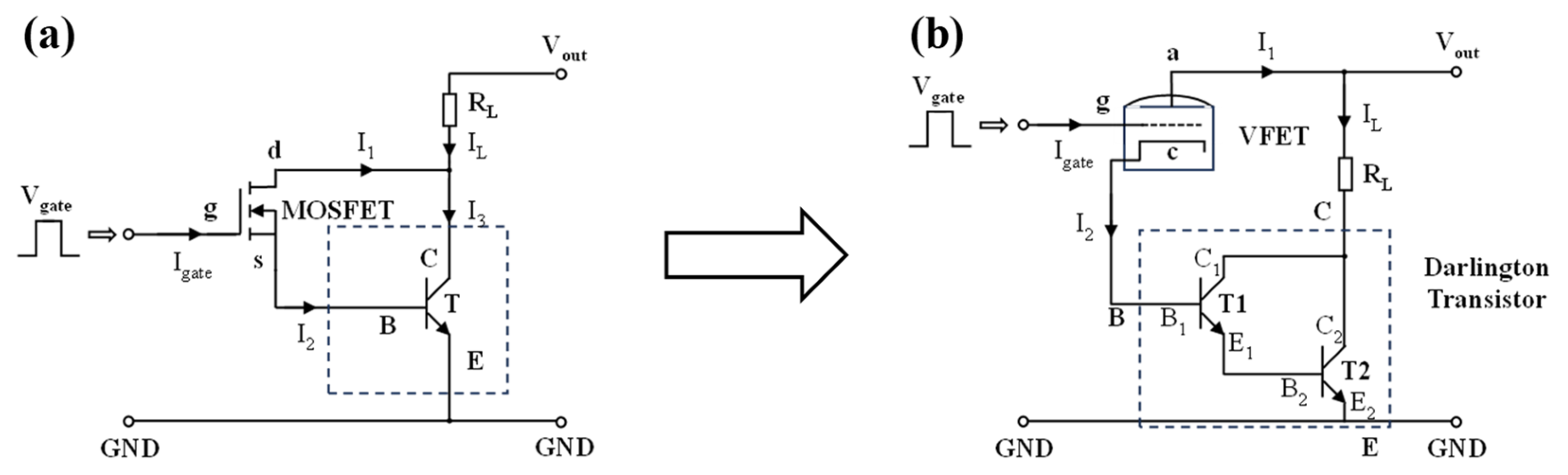
Firstly, the theoretical origin of the Miller effect is deduced. As demonstrated in Figure 1a,b, the well-known MOS–bipolar Darlington structure and the improved VFET–DT structure proposed in this paper are illustrated, respectively. In the VFET–DT structure, the load resistor (RL) is connected in parallel with the VFET device at the input terminal, rather than in series as in the traditional MOS–bipolar structure. This modification is predicated on the principle that the anode–cathode voltage Vac of the VFET remains essentially unaltered during both the on and off states.
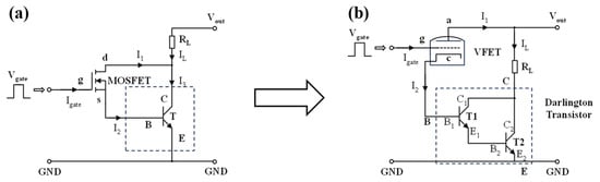
Figure 1.
Discrete Darlington switch of (a) MOS-bipolar structure and (b) VFET–DT structure.
The turn-on and turn-off behavior of both VFETs and MOSFETs is controlled by the gate voltage. The application of a drive voltage signal, designated as Vgate, to the gate g results in the emission of electrons from the cathode c of the VFET. These electrons accelerate across the vacuum beneath the high voltage at the anode and are subsequently collected by the anode a to form a field emission current. This process enables the VFET to conduct. The distinction between these two states is that, in the off state, the source–drain of a power MOSFET can withstand almost the entire forward voltage, while the conducting channel formed in the on state exhibits extremely low resistivity, with the forward voltage primarily acting on the load RL. The voltage drop between the cathode and anode of the VFET is not contingent upon the device’s on or off state. It can thus be concluded that, within the VFET–DT structure, anode a of the VFET is directly connected to the DC voltage source Vout, thus ensuring a high voltage is maintained for the purpose of efficient electron collection.
The output section employs a DT formed by cascading transistors T1 and T2 (within the dashed box), with the following output characteristics:
Here, β′ represents the equivalent current gain of the composite DT. The employment of multiple cascaded transistors at the output results in a higher gain than that achieved by a single transistor. The subsequent section will theoretically demonstrate the advantages of the improved VFET–DT structure.
The arrival of the gate signal Vgate voltage pulse results in the generation of currents I1 and I2 across the gate–anode and gate–cathode capacitances, Cga and Cgc, respectively, of the VFET. This process gives rise to the following set of equations:
Since VBE can be considered a constant, we have
Thus, the gate current Igate of VFET–DT is
In the MOS–bipolar structure illustrated in Figure 1a, the gate–source voltage Vgs exerts a negative feedback effect on the drain–source voltage Vds. The BJT amplifies the base input current signal, which is then fed back to the drain–source voltage Vds through the feedback loop involving RL:
The magnitude of AV is contingent on the load resistance RL and the feedback effect represented by the current gain β of the transistor T. It has been demonstrated that an increase in RL and β results in a more pronounced effect of Vgs on Vds through feedback, thereby increasing AV. It can thus be concluded that the gate current, Igate, of the MOS–bipolar structure is as follows:
Equation (8) illustrates the impact of the Miller effect on the input capacitance in the MOS–bipolar structure. The input capacitance Ciss measured with the source and drain shorted is equivalent to (Cgd + Cgs). However, due to the gate–drain capacitance Cgd bridging the input and output ends, it is amplified by a factor of (1 + AV) under feedback, thereby increasing the effective input capacitance when the circuit is turned on and turned off. The Miller effect extends the charging and discharging time of the input capacitance in the MOS–bipolar structures, resulting in a delay in the propagation of the gate voltage waveform during switching. This delay is known as the Miller plateau [21], and its presence can be observed in the rising and falling edges of gate voltage. In order to mitigate the impact of the Miller effect on the switching performance of the MOS–bipolar structure, it is imperative that the values of RL and β are not excessively high, thus avoiding the occurrence of excessive feedback.
A comparison of Equations (6) and (8) shows that under ideal conditions, the VFET–DT structure is free from the Miller effect, which indicates that the VFET–DT structure can achieve higher switching speed than the MOS–bipolar structure. In practice, the parasitic resistance of the transmission line and the BJT’s emitter junction resistance rbe will cause a certain voltage drop when the VFET is conducting. This will lead to fluctuations in the anode–cathode voltage Vac. However, given that Vac is high (typically over several hundred volts), the approximation of the ideal case remains valid. The VFET–DT’s inherent immunity to the Miller effect renders it well suited for high-power applications, enabling the design of high current gain β′ and high load resistance RL. Furthermore, the VFET, operating on the basis of field emission principles, exhibits a complete absence of leakage current in the off state. This configuration enables higher gain in the cascaded Darlington structure without the concern of amplifying both leakage and output currents, as seen in the MOS–bipolar structure. This feature suggests that the VFET–DT structure exhibits considerable potential for utilization in high-power applications.
3. Results and Discussion
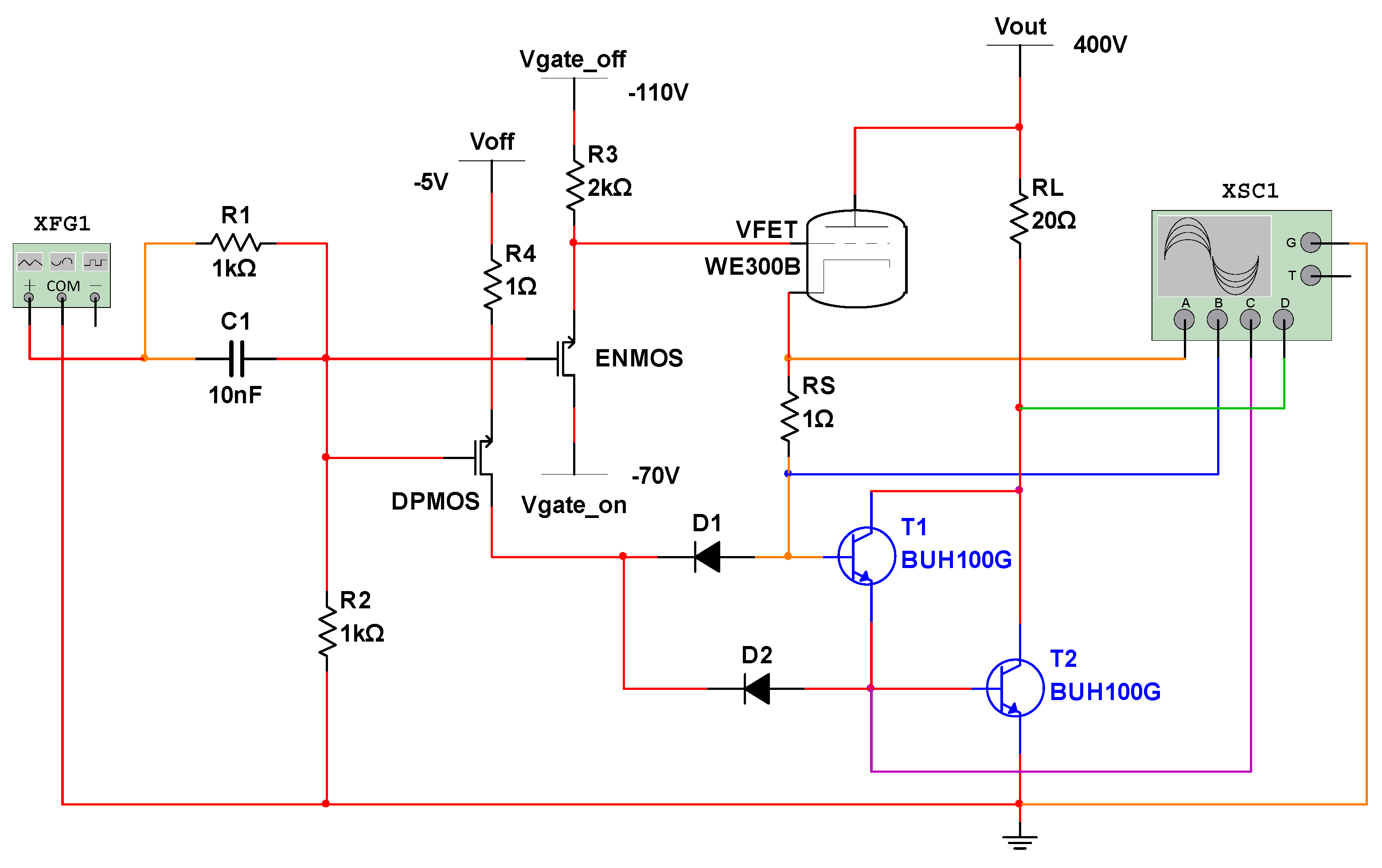
The construction of a power switch circuit based on the VFET–DT structure was undertaken using the Multisim software (Application version: 14.0.1 (14.0.1081), Database version: 14.0.b), as illustrated in Figure 2. The VFET and BJT components utilized in this study are derived from the Multisim database and are based on real electronic components that exist physically, rather than being purely modeled. A WE300B-type VFET is used on the input side (specific parameters are provided in Appendix A). A maximum cathode emission current of 200 mA can be achieved at the rated anode voltage of 650 V. The gate voltage is set to negative in order to prevent the electrons from being intercepted by the gate and forming a leakage gate current. Consequently, the input power consumption of the gate is essentially zero. A similar vacuum transistor planar structure using a carbon nanotube cold cathode was fabricated in our previous work [22]. The output end incorporates a bipolar Darlington transistor, which is arranged in a cascading configuration with transistors designated as T1 and T2 (transistor type: BUH100G; see Appendix A). A sampling resistor, designated as RS, is inserted between the VFET and transistor T1 with the objective of measuring the base drive current IB supplied by the VFET. BJTs exhibit a charge storage effect, which affects the overall turn-off speed of the device. By connecting external diodes D1 and D2 to provide a reverse drive current to the bases of T1 and T2, the removal of stored charges is accelerated, thereby improving the overall turn-off speed of the device.
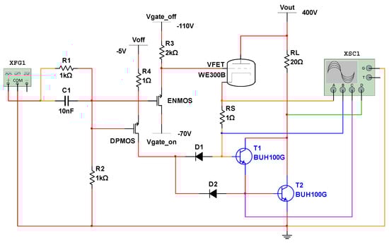
Figure 2.
Simulation circuit of a discrete VFET–DT switch.
The drive circuit can be subdivided into two sections. The gate voltage of the VFET (Vgate) is controlled by a branch containing an n-channel enhancement-type MOSFET, which switches levels under the signal from the function signal generator XFG1. Diodes D1 and D2 are connected to a p-channel depletion-type MOSFET, which in turn is connected to the negative voltage source Voff. The function of the MOSFET is to provide the reverse current required to turn off the drive transistors. The power consumption of the drive circuit is the source of power consumption at the input end, which is 0.85 W under DC conditions and 0.425 W under pulse conditions (with a duty cycle D = 50%). The simulation is based on the assumption that a default case temperature of 27 °C applies, on the premise that high-power BJTs are characterized by effective heat dissipation conditions. It is imperative to note that all parameters are set below the rated values to ensure that all components operate safely.
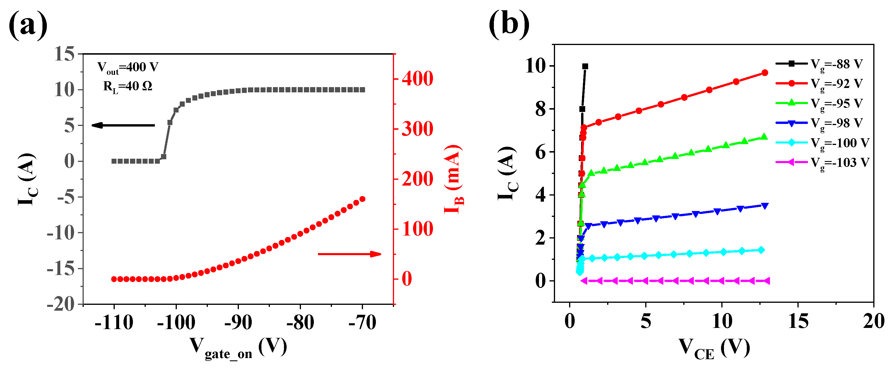
By replacing the XFG1 with a fixed 10 V DC voltage source, the static characteristics of the VFET–DT can be measured. Figure 3a illustrates the effect of varying the gate voltage Vgate_on on the output current IB of the VFET and the equivalent output current IC of the DT (the sum of the collector currents of T1 and T2). When Vgate_on is below −103 V, both IB and IC are essentially zero, indicating that the VFET–DT is turned off. As Vgate_on increases, IB exhibits an upward trend, reaching a maximum of 160 mA at Vgate_on = −70 V. Meanwhile, IC grows rapidly over the range of Vgate_on from −103 V to −88 V, then saturates at 10 A and remains constant regardless of any subsequent increase in Vgate_on. The VFET–DT is fully turned on at this point. It demonstrates that the VFET–DT exhibits excellent switching characteristics, with the capacity to switch between a narrow gate voltage range.
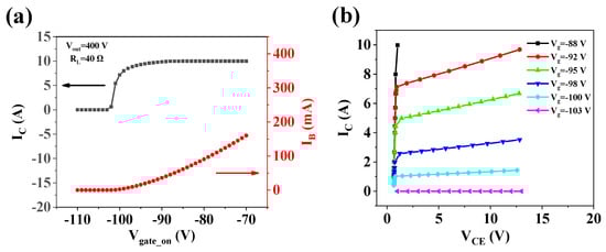
Figure 3.
I-V characteristics of VFET–DT: (a) transfer characteristic curve: plot of output current IC and base current IB of DT vs. driven gate voltages Vgate_on when Vout = 400 V and RL = 40 Ω; (b) output characteristic curve: plot of output current IC vs. forward voltage drop VCE.
Figure 3b illustrates the output characteristic of the VFET–DT, showing the relationship between the output current IC and the forward voltage drop VCE. For different gate voltages Vgate_on, the IC–VCE curves exhibit different operating modes of the DT. In the event of Vgate_on being set to −103 V, the DT operates in the cutoff region with IC fixed at 0. This indicates that the VFET–DT is in the off state. In the event of Vgate_on being set to −88 V, the DT operates in the saturation region, with VCE falling below 1 V. In this case, IC rises sharply with increasing VCE, and the IC–VCE curve is not controlled by Vgate_on. This indicates that the VFET–DT is in the on state. When Vgate_on is between −103 V and −88 V, IC gradually reaches a steady value as VCE increases. The maximum current that IC can reach is mainly determined by Vgate_on. During this phase, DT enters the active region, corresponding to the switching process of the VFET–DT. At this stage, both VCE and IC are relatively high, and the switching losses generated are the main source of power consumption for the VFET–DT.
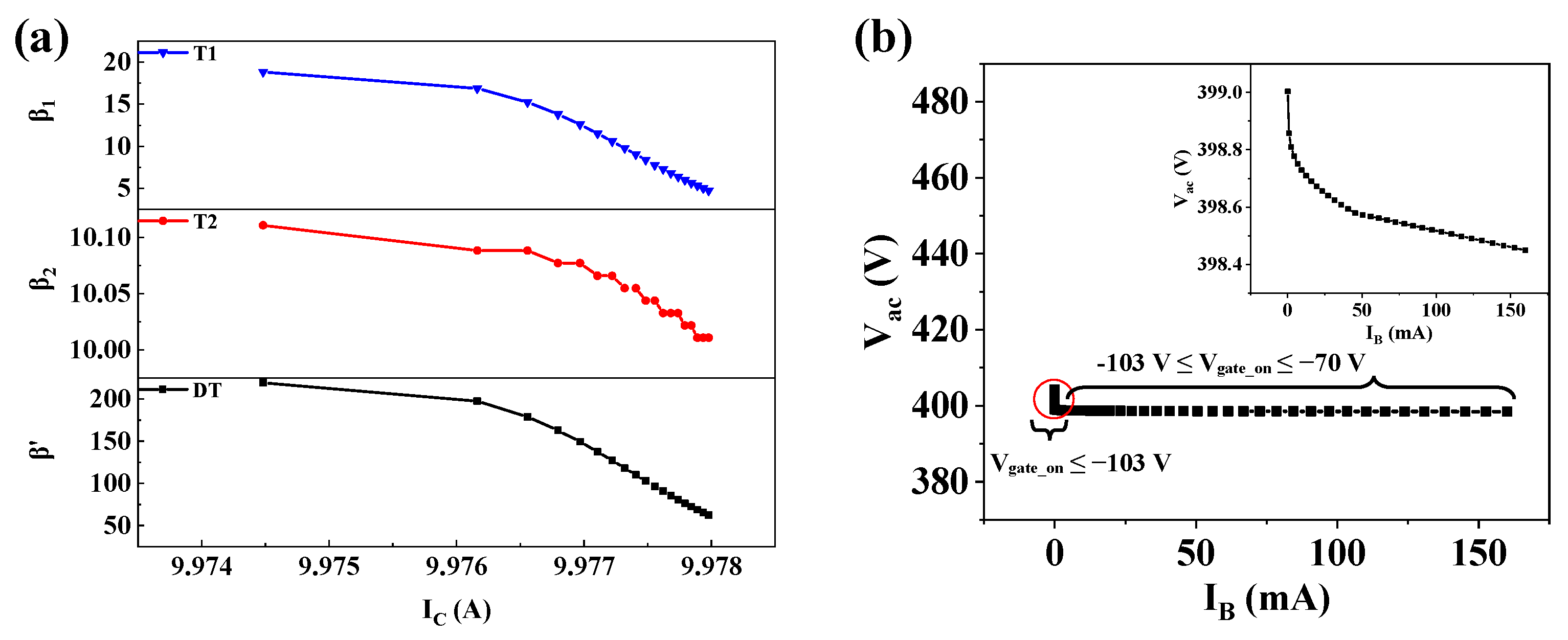
The operating characteristics of the internal components of the VFET–DT were measured at Vout = 400 V and RL = 40 Ω (see Figure 4). The relationship between the current gains β1 and β2 of transistors T1 and T2 and the output current IC of the VFET–DT is shown in Figure 4a. The current gain β′ of the DT is determined by β1 and β2 according to Equation (1). As IC decreases from 9.978 A to 9.974 A, β1 increases rapidly from 4.76 to 18.84, while β2 remains stable at around 10. This phenomenon can be attributed to the decrease in IB, which causes a transition from the saturation region to the active region for T1. Consequently, this transition leads to a significant rise in β1. In the Darlington structure, the collector–base voltage of T2 is equivalent to the collector–emitter voltage of T1, so the collector junction of T2 remains reverse-biased. Therefore, it can be concluded that T2 always operates within the active region. The reduction in IB is compensated by the gain of T1, resulting in a relatively stable β2. It is evident that the cascaded amplification of T1 and T2 gives the DT a maximum current gain of β′ = 220 under steady-state conduction conditions at IC = 9.97 A.
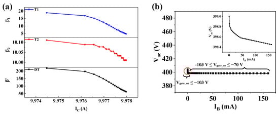
Figure 4.
Operating characteristics of the components of VFET–DT: (a) current gain of T1, T2, and DT at different collector current levels when Vout = 400 V and RL = 40 Ω; (b) output characteristic curve of VFET: plot of anode–cathode voltage Vac vs. output current IB at different driven gate voltages Vgate_on.
The output characteristic of the VFET is shown in Figure 4b. The influence of the parasitic resistance of the transmission line can be estimated by setting a sampling resistor RS (assuming RS = 1 Ω). When Vgate_on is below −103 V, there is no output current IB of the VFET. The induced potential at the cathode decreases slightly with the reduction in Vgate_on, and the anode–cathode voltage Vac reaches a maximum of 404.3 V (indicated by the red circle). As Vgate_on exceeds −103 V and continues to increase, the VFET turns on, IB gradually increases, and the voltage across RS rises, causing Vac to decrease. The inset in Figure 4b shows the Vac–IB curve under the on-state conditions (a local enlargement excluding the red circle), where the drop in Vac becomes progressively smaller as IB increases. The results have demonstrated that Vac remains essentially around 400 V in both the on and off states of the VFET. Therefore, Equation (5) is still approximately valid when the transmission line parasitic resistance is less than 1 Ω.
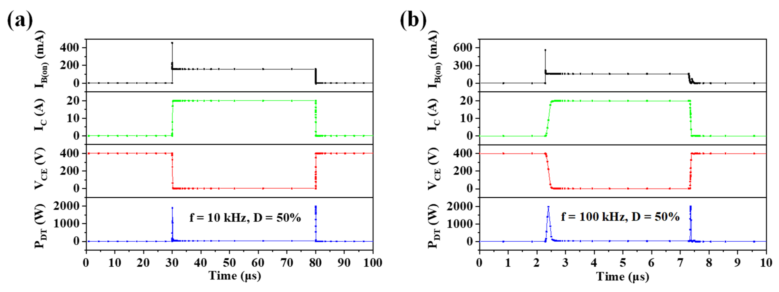
The dynamic characteristics of the VFET–DT were measured at a duty cycle of D = 50% and a frequency of f = 10 kHz and 100 kHz. The load resistance RL was set to 20 Ω in order to achieve higher output power under the pulse-driven conditions, and the gate voltages Vgate_on and Vgate_off were set to −70 V and −110 V, respectively. The waveform of the VFET output current IB(on) was measured via the voltage across RS (as shown by the black line in Figure 5), which describes the on-state drive current at the base of the DT. The base current IB is 0.158 A during the steady on state of the VFET. The overshoot and oscillations on the rising and falling edges of the IB(on) waveform are due to the cathode–gate capacitance, Cgc, of the VFET. The average power dissipation of VFET is 31.6 W at D = 50%, with the majority of this dissipation occurring during the on state and being irrelevant to the switching process. As a trade-off for eliminating the Miller effect, the output current of the VFET is not fully utilized by the load resistance RL, which reduces the energy conversion efficiency of Vout. However, the drive loss of the gate input terminal remains low at 0.425 W at D = 50% due to the absence of the Miller effect, ensuring the reliability of the small-signal drive circuit even under high-speed switching conditions.
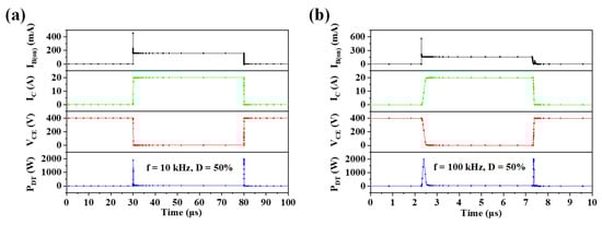
Figure 5.
Dynamic characteristics of VFET–DT at (a) f = 10 kHz and D = 50% and (b) f = 100 kHz and D = 50%.
During the on state of the VFET–DT, a maximum output current of ICM = 19.93 A and a minimum forward voltage drop of VCE(sat) = 1.316 V can be achieved in the IC and VCE waveforms (green and red lines in Figure 5). In the off state of the VFET–DT, IC turns to zero, and all of Vout is applied to the VFET–DT. This phenomenon results in a maximum VCE = 400 V. The rising and falling edges of the IC and VCE waveforms become smoother as f increases from 10 kHz to 100 kHz. This observation means that the delay time of the switching process increases. The widths of the rising and falling edges of the VCE waveform in Figure 5 were measured, and the corresponding delay times in the turn-on and turn-off processes are shown in Table 1. The power dissipation waveform of the DT (PDT, blue line in Figure 5) can be obtained by multiplying the IC and VCE waveforms, and the average power loss of DT is obtained by integrating the PDT waveform over a single period and dividing by the period duration. The average power loss of the DT is 16.2 W at f = 10 kHz and 43.1 W at f = 100 kHz, which is less than the total dissipation (PD = 100 W) of a single BJT.

Table 1.
Dynamic characteristics of VFET–DT.
The base–emitter voltage waveforms VBE1 and VBE2 of transistors T1 and T2 are illustrated in Figure 6. The waveform VBE1 is modulated by the waveform IB(on), as illustrated in Figure 5, for which they exhibit a comparable morphology. The overshoot spikes in the rising edge of waveform VBE1 and IB(on) are caused by the charging behavior of the parasitic capacitance of VFET (see Appendix A). The base and emitter of T1 are connected to Voff through diodes D1 and D2, respectively. During the turn-off period, the potentials of the base and emitter of T1 are identical, resulting in the value of VBE1 being zero. However, during the turn-off period, VBE2 is −4.3 V (with a diode D2 voltage drop of 0.7 V), for which in the T2, the emitter is grounded while the base is connected to Voff. Consequently, both transistors T1 and T2 are in the cutoff region when VFET–DT is in the off state. When the VFET–DT is in the on state, both VBE1 and VBE2 are 0.16 V, indicating that the emitter junctions of T1 and T2 are forward-biased. As was discussed in the preceding paragraph, transistors T1 and T2 function in the saturation region and the active region, respectively.
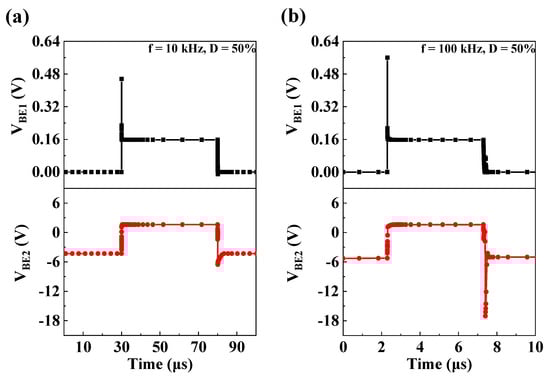
Figure 6.
Base-emitter voltage VBE waveforms of T1 and T2 at (a) f = 10 kHz and D = 50% and (b) f = 100 kHz and D = 50%.
4. Conclusions
A novel VFET–DT structure, which integrates a VFET and a DT with the advantages of gate voltage control, large power capacity, and high frequency, was introduced. The configuration, theory, and simulation results of the static/dynamic characteristics of the VFET–DT were reported. Through mathematical derivation, it was proven that the immunity to the Miller effect of VFET–DT is superior to the traditional MOS–bipolar structure in high-frequency applications. Taking advantage of this, the VFET–DT was able to operate over a wide frequency range from DC to 100 kHz while maintaining a high-power capability of 20 A and 400 V. The low forward voltage drop VCE(sat) and short delay time allow the VFET–DT device to have a low power dissipation of 75.125 W at a high switching frequency of 100 kHz. The results demonstrated that the combination of vacuum and solid-state transistors enhances the performance of the power switch. This would make it suitable for applications requiring high-voltage transformation and high-frequency conversion, such as industrial control, automotive electronics, and home appliances. Further experimental verification of the performance of the VFET–DT structure will be carried out in the near future.
Author Contributions
Conceptualization, Y.D. and Y.Z.; methodology, Y.D. and Y.Z.; software, Y.D.; validation, Y.D.; formal analysis, Y.Z.; investigation, Y.D.; resources, Y.Z.; data curation, Y.Z.; writing—original draft preparation, Y.D.; writing—review and editing, Y.Z.; visualization, Y.D.; supervision, Y.Z.; project administration, Y.Z.; funding acquisition, Y.Z., S.D., J.S. and Y.K. All authors have read and agreed to the published version of the manuscript.
Funding
This work was funded by the National Natural Science Foundation of China (grant Nos. 62274188 and U22A2020), the National Key Basic Research Program of China (grant No. 2019YFA0210201), the Guangdong Basic and Applied Basic Research Foundation (grant No. 2023A1515011876), the Science and Technology Department of Guangdong Province, and the Fundamental Research Funds for the Central Universities.
Data Availability Statement
All relevant data are available from the corresponding author on reasonable request.
Conflicts of Interest
All authors declare that they have no conflicts of interest.
Appendix A
The electrical data of the VFET and BJT used for the discrete Darlington in simulation circuits are below.
| VFET | WE300B and STC4300B | |
| Anode–Cathode Voltage Vac | 0–650 V | |
| Gate–Cathode Voltage Vgc | 0–−160 V | |
| Cathode Current Ic | 0–200 mA | |
| Gate–Cathode Capacitance Cgc | 9.0 pF | |
| Gate–Anode Capacitance Cga | 15 pF | |
| Anode–Cathode Capacitance Cac | 4.3 pF | |
| BJT | BUH100G and TO-220-3 | |
| Collector–Emitter Sustaining Voltage VCEO | 400 V | |
| Continuous Collector Current IC | 10 A | |
| Peak Collector Current IC | 20 A | |
| Current Gain β (typ) at IC = 10 A and VCE = 5 V | 9.5 | |
| Total Dissipation PD at TC = 25 °C | 100 W |
References
- Tao, H.; Wang, Q. Study on Ballistic Transport Electronics—A Vacuum Field Emission Transistor with Carbon Nanotube Cold Cathode. In Proceedings of the 2023 24th International Vacuum Electronics Conference (IVEC), Chengdu, China, 25–28 April 2023; pp. 1–2. [Google Scholar]
- Chern, W.; Rughoobur, G.; Zubair, A.; Karaulac, N.; Cramer, A.; Gupta, R.; Palacios, T.; Akinwande, A. Demonstration of a ~40 kV Si Vacuum Transistor as a Practical High Frequency and Power Device. In Proceedings of the 2020 IEEE International Electron Devices Meeting (IEDM), San Francisco, CA, USA, 12–18 December 2020; pp. 5.2.1–5.2.4. [Google Scholar]
- Ulisse, G.; Brunetti, F.; Ciceroni, C.; Gemma, F.; Dispenza, M.; Fiorello, A.M.; Ricci, F.; Di Carlo, A. A Multifinger Microtriode with Carbon Nanotubes Field Emission Cathode Operating at GHz Frequency. Nanotechnology 2015, 26, 215204. [Google Scholar] [CrossRef] [PubMed]
- Luo, Y.; Zhang, J.; Alexandrov, P.; Fursin, L.; Zhao, J.H. Fabrication and Characterization of High Current Gain (β = 430)and High Power (23 A–500 V) 4H-SiC Hybrid Darlington Bipolar Transistor. IEEE Trans. Electron Devices 2004, 51, 2211–2216. [Google Scholar] [CrossRef]
- Ma, S.; Wang, K.; Zhang, M.; Ma, K. Design of a 2.4-GHz MEMS-Based Oscillator With Dynamic Self-Body-Biasing Scheme and Darlington Cell. IEEE Trans. Microw. Theory Tech. 2024, 72, 618–627. [Google Scholar] [CrossRef]
- Biswas, S.K.; Basak, B. Some Aspects in the Design of Discrete MOS-Bipolar Darlington Power Switches. IEEE Trans. Ind. Appl. 1991, 27, 340–345. [Google Scholar] [CrossRef]
- Luo, P.; Madathil, S.N.E.; Nishizawa, S.-I.; Saito, W. Turn-OFF dV/Dt Controllability in 1.2-kV MOS-Bipolar Devices. IEEE Trans. Power Electron. 2021, 36, 3304–3311. [Google Scholar] [CrossRef]
- Deng, X.; Cheng, Z.; Chen, Z.; Wu, H.; Bai, S.; Li, X.; Li, X.; Chen, W.; Zhang, B. A Hybrid-Channel Injection Enhanced Modulation 4H-SiC IGBT Transistors With Improved Performance. IEEE Trans. Electron Devices 2022, 69, 4421–4426. [Google Scholar] [CrossRef]
- Wu, W.; Li, Y.; Yu, M.; Gao, C.; Shu, Y.; Chen, Y. Low Switching Loss Built-In Diode of High-Voltage RC-IGBT with Shortened P+ Emitter. Micromachines 2023, 14, 873. [Google Scholar] [CrossRef] [PubMed]
- Abdalgader, I.A.S.; Kivrak, S.; Özer, T. Power Performance Comparison of SiC-IGBT and Si-IGBT Switches in a Three-Phase Inverter for Aircraft Applications. Micromachines 2022, 13, 313. [Google Scholar] [CrossRef] [PubMed]
- Yeon, J.; Ul Ain Akbar, S.Q. A Reverse-Conducting IGBT Enabling High Switching Frequency up to 60 kHz for PFCs in Home Appliances. In Proceedings of the 2021 23rd European Conference on Power Electronics and Applications (EPE’21 ECCE Europe), Ghent, Belgium, 6–10 September 2021; pp. 1–9. [Google Scholar]
- Wakui, S.; Yano, K. Darlington Power Switches Using Si-SJBJT and SiC-MOSFET. IEEJ J. Ind. Appl. 2025, 14, 293–300. [Google Scholar] [CrossRef]
- Kobayashi, K.W. Linearized Darlington Cascode Amplifier Employing GaAs PHEMT and GaN HEMT Technologies. IEEE J. Solid-State Circuits 2007, 42, 2116–2122. [Google Scholar] [CrossRef]
- Weng, S.-H.; Chang, H.-Y.; Chiong, C.-C.; Wang, Y.-C. Gain-Bandwidth Analysis of Broadband Darlington Amplifiers in HBT-HEMT Process. IEEE Trans. Microw. Theory Tech. 2012, 60, 3458–3473. [Google Scholar] [CrossRef]
- Yang, Y.M.; Lin, X.Q.; Dong, J.S.; Hao, P.; Mei, P. A Fully Integrated Darlington-Cascode Distributed Amplifier With m-Derived Matching Sections. IEEE Microw. Wirel. Technol. Lett. 2024, 34, 524–527. [Google Scholar] [CrossRef]
- Zhang, J.; Wang, Z.; Ma, C. A CMOS Transimpedance Amplifier with Broad-Band and High Gain Based on Negative Miller Capacitance. Integration 2023, 91, 60–66. [Google Scholar] [CrossRef]
- Zhang, B.; Wang, S. Miller Capacitance Cancellation to Improve SiC MOSFET’s Performance in a Phase-Leg Configuration. IEEE Trans. Power Electron. 2021, 36, 14195–14206. [Google Scholar] [CrossRef]
- Tan, J.; Zhu, Y.; Lu, S.; Yu, Q. Modeling of Input Capacitance of IGBTs under Dynamic Conditions. Int. J. Circuits Syst. Signal Process. 2017, 11, 157–161. [Google Scholar]
- Wu, R.; Blaabjerg, F.; Wang, H.; Liserre, M.; Iannuzzo, F. Catastrophic Failure and Fault-Tolerant Design of IGBT Power Electronic Converters—An Overview. In Proceedings of the IECON 2013-39th Annual Conference of the IEEE Industrial Electronics Society, Vienna, Austria, 10–13 November 2013; pp. 507–513. [Google Scholar]
- Huang, H.; Wu, J.; Xu, W.; Lu, T. The Influence of Driving Parameters on Conducted EMI for an IGBT Module. IEEE Trans. Electromagn. Compat. 2020, 62, 2285–2293. [Google Scholar] [CrossRef]
- Liu, S.; Song, S.; Xie, N.; Chen, H.; Wu, X.; Zhao, M. Miller Plateau Corrected with Displacement Currents and Its Use in Analyzing the Switching Process and Switching Loss. Electronics 2021, 10, 2013. [Google Scholar] [CrossRef]
- Jiang, J.; Gao, J.; Liang, J.; Ding, Y.; Ou, H.; Ke, Y.; She, J.; Zhang, Y.; Deng, S. An On-Chip Carbon-Nanotube Field Emission Array with Self-Focusing on Wafer. Carbon 2025, 238, 120206. [Google Scholar] [CrossRef]

Disclaimer/Publisher’s Note: The statements, opinions and data contained in all publications are solely those of the individual author(s) and contributor(s) and not of MDPI and/or the editor(s). MDPI and/or the editor(s) disclaim responsibility for any injury to people or property resulting from any ideas, methods, instructions or products referred to in the content. |
© 2025 by the authors. Licensee MDPI, Basel, Switzerland. This article is an open access article distributed under the terms and conditions of the Creative Commons Attribution (CC BY) license (https://creativecommons.org/licenses/by/4.0/).