Article

Two-Dimensional Fin-Shaped Carbon Nanotube Field Emission Structure with High Current Density Capability

State Key Laboratory of Optoelectronic Materials and Technologies, Guangdong Province Key Laboratory of Display Material and Technology, School of Electronics and Information Technology, Sun Yat-sen University, Guangzhou 510275, China
*
Authors to whom correspondence should be addressed.
Electronics 2025, 14(7), 1268; https://doi.org/10.3390/electronics14071268
Submission received: 26 February 2025 / Revised: 17 March 2025 / Accepted: 20 March 2025 / Published: 24 March 2025
(This article belongs to the Special Issue Vacuum Electronics: From Micro to Nano)

Abstract

:
A vacuum electron device requires a high-performance electron source that provides high current and current density. A carbon nanotube (CNT) field emission cold cathode is the optimal choice. To achieve its higher emission current capacity, its macroscale and microscale structures should be combined. Here, a two-dimensional fin-shaped CNT field emission structure is proposed, integrating a macroscale CNT fin with billions of nanoscale nanotubes. The fin contributes two-dimensional heat dissipation paths, and the nanotubes provide a high field enhancement factor, both of which enhance the high-current field emission characteristics. A model combining macro- and microstructures was simulated to optimize the structure and fin-shaped array parameters. The calculation of the field enhancement factor of the compound structure is proposed. It was also determined that the fin-shaped array configuration can be densely arranged without field screen effects, thereby enhancing the emission area efficiency. The fin-shaped CNT emitter and array emitters with different parameters were fabricated by laser ablation, which demonstrated superior field emission characteristics. A 16.55 mA pulsing emission current, 1103.33 A/cm2 current density, and 6.13% current fluctuation were achieved in a single fin-shaped CNT emitter. An 87.29 mA pulsing emission current, 0.349 A/cm2 current density, and 1.9% current fluctuation were achieved in a fin-shaped CNT array. The results demonstrate that the high-current field emission electron source can be realized in a well-designed emission structure that bridges the nanoscale emitter and macroscale structure.

1. Introduction

Carbon nanotubes (CNTs) have been proven to be excellent field emission materials, and CNT cold cathodes have been applied in several kinds of vacuum electronic device (VED) prototypes such as X-ray tubes [1,2], gyrotrons [3], and back-wave oscillators [4,5], etc., demonstrating significant advantages, including room temperature operation, fast turn-on time, small size, and narrow energy distribution [6]. Such types of VEDs all require high current and high current density to boost their power performance based on the power law P = IV. At a fixed voltage, the current and current density are proportional to power. Regarding device application, the primary target is to increase the emission current and current density of the CNT cathode.
As a one-dimensional nano-emitter, the CNT cathode predominantly fails due to Joule heating-induced vacuum breakdown in high current density working situations [7,8,9,10]. The heat generated from its emission tip and body has to be transported along the axis of the tube to the substrate, which is not sufficient and causes a temperature ramping that burns out the CNT. As a thin-film emitter, densely arranged CNTs experience a serious electric field screening effect, which reduces the field enhancement at their tips [11,12]. To avoid this, the CNT pattern array has been regularly designed to separate the CNTs one by one [13,14,15]. The best ratio of CNT length to spacing was deemed to be 1:2 to avoid the screening effect [16,17]. In addition, the emitters are designed with a large height-to-diameter ratio (>10) to achieve a high field enhancement factor [18,19]. The combination of these two strategies raises another problem: the large spacing occupies a large area that does not contribute to field emission. Although CNT arrays can emit a uniform field emission current at low electric fields, their relatively small effective emission area limits their ability to achieve higher current and current density.
In macroscale device applications, the cathode has a large area on the order of mm2 or cm2. Meanwhile, the one-dimensional emitter has a nanoscale structure and morphology. To take advantage of the nanotip field enhancement factor and fully utilize the whole surface area, it is necessary to design a field emission structure that combines macroscale and nanoscale features, thereby maximizing the advantages of each and avoiding their drawbacks.
Here, a two-dimensional fin-shaped CNT field emission structure is proposed. The vertically aligned CNTs are densely arranged in a straight line to form a fin shape. The whole fin-shaped CNT acts as a two-dimensional emitter that combines a macrostructure fin and nanostructure CNTs. The first advantage is that the top of the CNT fin forms a two-dimensional continuous line shape that arranges more emission sites without gaps, fully using the line area. At the same time, the screening effect is minimal because the sharp fin inherently possesses a field enhancement factor. The second advantage is that the sidewall of the CNT fin is a two-dimensional surface, which provides a large area for heat dissipation. The heat generated at the top of the fin can dissipate through two-dimensional pathways, reducing the temperature rise in the CNT body. Therefore, the fin can effectively prevent the destruction of the CNT and maintain a large emission current capacity. In addition, the fin shape is also an ideal cathode structure for specified device applications [20,21]. For example, the sheet electron beam is popular for the terahertz traveling wave tube and back-wave tube [22,23,24].
In this paper, the fabrication of the fin-shaped CNT structure is introduced. The field emission characteristics were measured to achieve high current and current density. The fin-shaped CNT array was also designed. The relationships among the structural parameters, field enhancement factors, electrostatic field distribution, and thermal transport ability were simulated. An optimal structure parameter for the fin-shaped CNT array, including fin height and spacing between fins, was achieved. It was found that the spacing of the macro-emitter could be reduced to match that of the nanostructures, which means that macro-emitters with a high height–diameter ratio could be distributed as densely as the tiny emitters. In addition, a simulation method combining macrostructure and nanostructure was introduced to improve simulation accuracy over multiple scales.

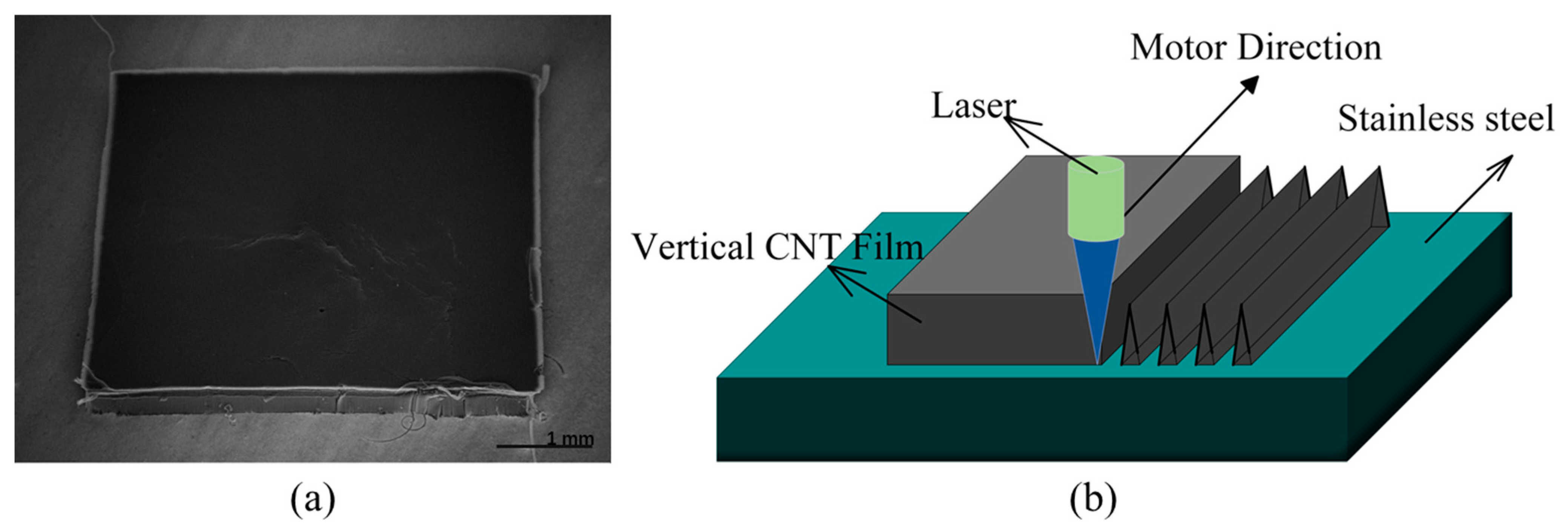
2. Materials and Methods
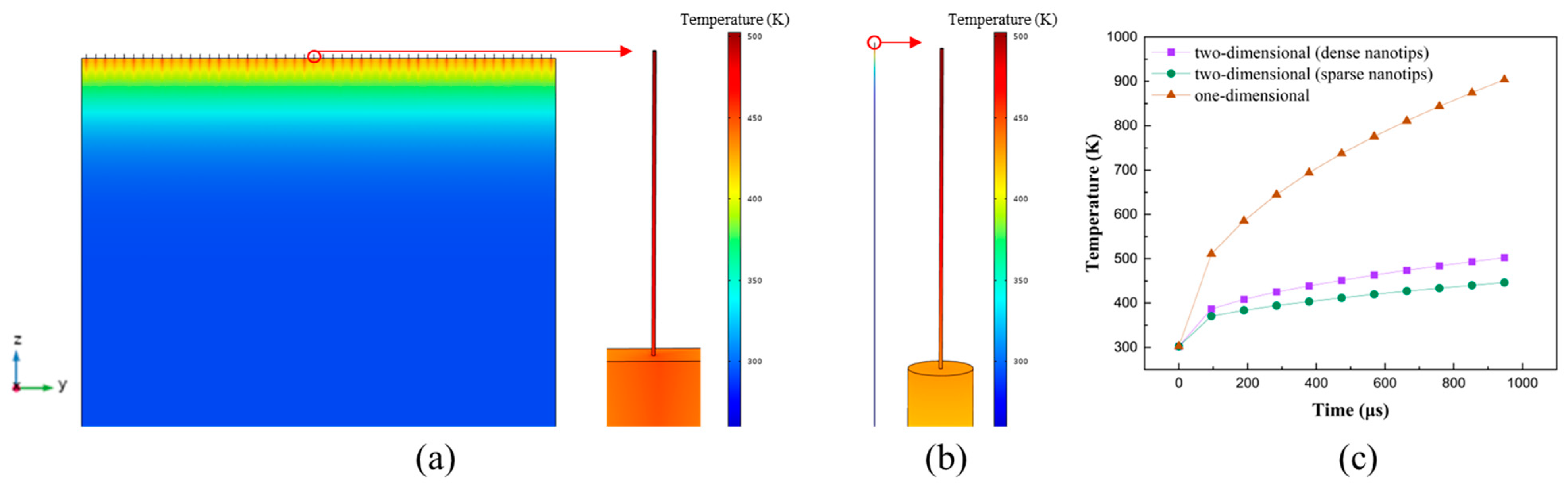
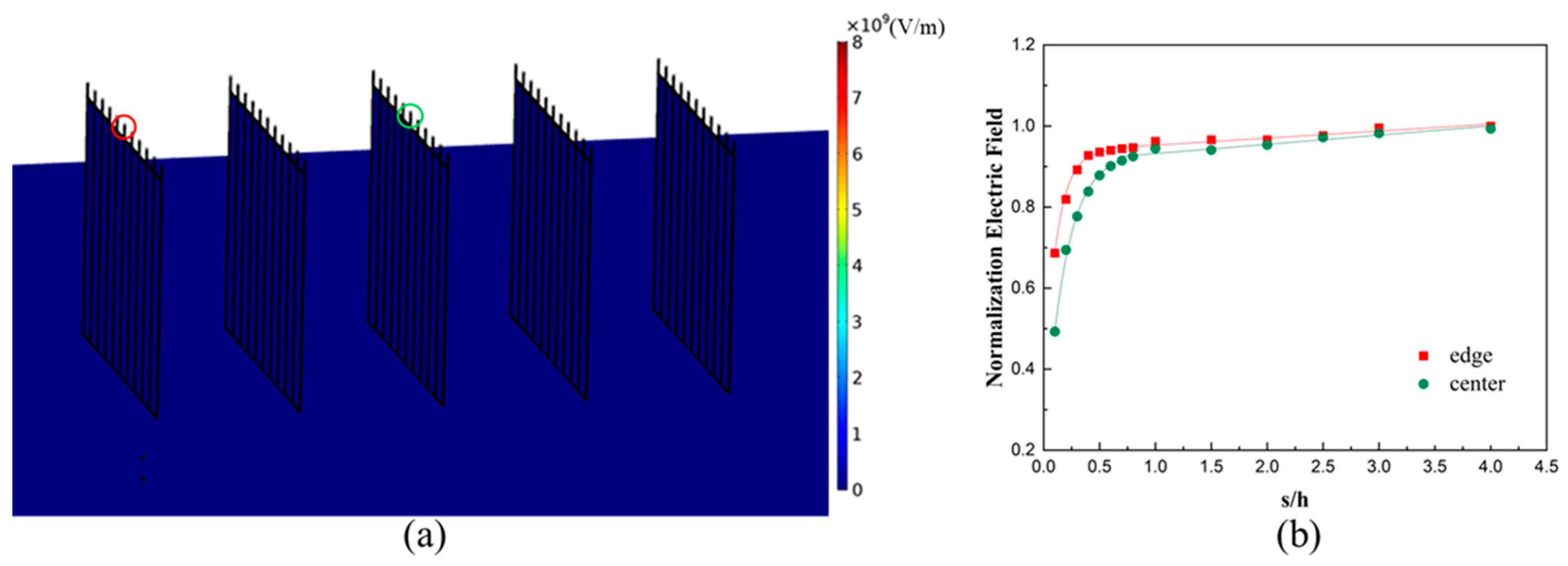
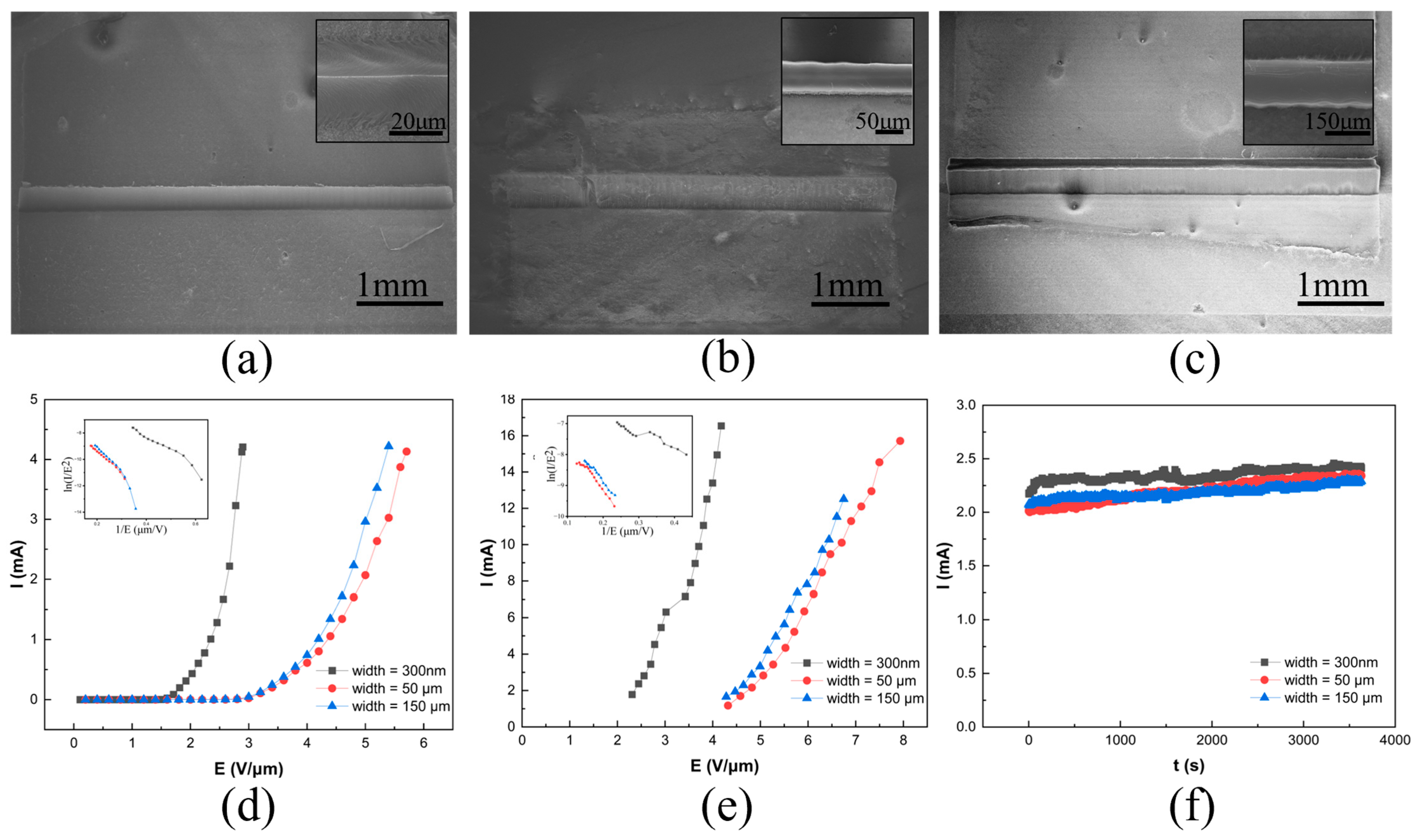
The fabrication methods for a fin-shaped CNT emitter can vary. In this work, a laser ablation method was introduced. Firstly, a macroscale 5 mm × 5 mm in area, 500 μm in height, vertically aligned multi-walled CNT thick film was synthesized on a planar quartz substrate by thermal chemical vapor deposition, as shown in Figure 1a. Secondly, the CNT thick film was transferred to a conductive stainless-steel substrate using conductive silver paste. Then, a power pulsing laser illuminated the interface of the CNT and quartz substrate to detach the CNT film from the quartz. Thirdly, a focused laser with focal spots of approximately 160 μm was employed to ablate the CNT films along a predetermined motion trajectory, as shown in Figure 1b. Consequently, the designed pattern on the CNT film can be obtained. In this work, a fin-shaped CNT was ablated. By modifying the laser motion path, the fin-shaped CNT with widths of 0.3 μm, 50 μm, and 150 μm, and fin-shaped CNT arrays with spacings of 160 μm, 360 μm, and 600 μm were fabricated.
The morphologies of the fin-shaped CNT emitters and fin-shaped CNT array emitters were observed using scanning electron microscopy (SEM, ZEISS Supra 55, Oberkochen, Germany). Field emission characteristics were measured in an ultra-high vacuum chamber at a pressure of 9 × 10⁻⁶ Pa. A diode test structure was adopted with a gap of 200 μm between the cathode and anode. Both the DC and pulsing field emission characteristics were measured to determine the maximum current and current density. To avoid heat-induced outgassing of the silver paste due to electron bombardment at the anode, a water-cooling heatsink was installed at the back of the anode plate to facilitate heat dissipation. The three-dimensional electrostatic field distributions of various parameters and heat transfer capacities were calculated using COMSOL Multiphysics software(Version 5.4).

3. Results

A fin-shaped CNT was ablated by a laser, and its morphology is shown in Figure 2a. The fin has a length of 5000 μm, a height of 280 μm, and a width of 300 nm. At the top of the fin, many nanotube tips protrude upwards, with a typical height of several micrometers and a diameter of 10 nm, as shown in Figure 2b. It is a compound structure with macro fins and nanotubes, spanning five orders of magnitude in dimensions. The fin acts as a base for heat dissipation and electron transport, while the nanotubes act as emission tips with a high field enhancement factor. Based on its morphological characteristics, a model was built to simulate the intensity and distribution of the electrostatic field at the top of the structure.
The simulation model consists of two parts, as shown in Figure 2c–e. One is a macro fin (the blue part in Figure 2c,d) with a length of 400 μm, a height of 280 μm, and a width that varies. The second component is a nanocylinder (the red part in Figure 2c,d) with a height of 20 μm and a diameter of 10 nm, representing the nanotube. Along the top of the fin, the nanotubes are densely arranged with 2 μm spacing in the width direction and 40 μm spacing in the length direction. The gap between the cathode and anode in the model was 200 μm. In simulations, the three-dimensional finite element method faces significant challenges in establishing grids when the size of macrostructures exceeds three orders of magnitude compared to microstructures. Considering the accuracy of the calculated results, the grids in the nanostructures are designed to be quite small, and the grids at the interface of macro- and nanostructures are similarly small to maintain the grids’ continuity. The large inner grids in the macrostructure are difficult to be compatible with these grids at the interface. To solve this problem, the methodology employed involved the construction of several dense one-dimensional segments at the interface. Then these segments were isometrically mapped to the nanostructure and continuously mapped to the macroscopic structure with proportional increases to create two-dimensional grids on a fin, nanocylinders, and computational domains. Ultimately, the two-dimensional grids were scanned to three dimensions at a specific size. It is noted that the cross-sectional shape of the fin was set as a rectangle in the simulation, while its actual shape was a triangular prism. The reason was that the bottom shape of the fin had less effect on its field enhancement factor. This simplification does not change the simulation results.
The number of nanocylinders in the width direction increased with the width of the fin. To explore the influence of the two structures on the field enhancement factor, they were calculated separately as a fin and as a long nanotube and then as a whole. The field enhancement factor β is defined as the ratio of the simulated electric field at the top of the nanotube to the macro electric field at the cathode–anode gap, which is equal to the voltage divided by the cathode–anode distance. The results are shown in Figure 2d. By comparing the products of the field enhancement factors of two independent structures with the field enhancement factor of their compound, the field enhancement factor of the compound βc can be expressed as follows:
β c α β a β i ,
where α is an effective coefficient ranging from 0.85 to 0.95, βa is the field enhancement factor of the macrostructure, and βi is the field enhancement factor of nanostructures. The dominant influence of βc on the compound structure originates from the nanotips. All three β values exhibit a rapid decline as the width of the fin increases from 1 μm to 50 μm, after which they stabilize near a constant value as the width increases from 50 μm to 500 μm. The decline in βa is attributed to the fin becoming a cube as its width increases. The decline in βi is attributed to the enhancement of electric field screening produced between the nanostructures with an increase in their numbers.
Heat transport in the CNT cathode is mainly caused by heat conduction because heat radiation in the vacuum is negligible. In a fin-type CNT film, the two-dimensional heat transport path possesses more efficient heat transport properties than the one-dimensional path in a single CNT. A heat transport simulation of a fin-shaped CNT emitter was also carried out using a compound fin model, as shown in Figure 3a. The fin had a length of 400 μm, a height of 298 μm and a width of 200 nm, which simulated the fin-shaped CNT film, while inside the fin, the nanostructures had a height of 300 μm, a radius of 10 nm, and spacings of 4 μm and 8 μm, simulating the CNT emitting tip in a vertical CNT film. For comparison, a one-dimensional model (Figure 3b) was established. The one-dimensional model had a macro cylinder with a height of 298 μm, a radius of 100 nm, and the same nanostructure as that in the fin. The heat conductivity coefficients of the nanostructure and the fin were set to different values because the heat conductivity along the CNT and between the CNTs is different. The heat conductivity coefficient in the nanostructure was set to 3000 W/(m·K) as the ideal CNT due to its ballistic heat transport along the tube [25]. In the fin, it was set to 3 (W/m·K) because the heat transport from tube to tube was weak due to the effect of phonon scattering caused by defects and carbon pollution [26]. The top surface of the nanostructure was set as the heat source to simulate the Joule heat generated during field emission from protruding CNTs. The heating power was calculated using the equation P = I2R. The current I was set to 100 μA, and the resistance R was set to 200 Ω for each CNT to simulate the temperature runaway under high-current conditions. The specific heat capacity was set to 710 J/(Kg·K). The nanostructure density was set to 1500 Kg/m3, which equals the density of a single CNT, and the fin density was set to 400 Kg/m3, reflecting the lower density of a CNT film due to the presence of gaps between CNTs. All parameters were based on reported studies [25,26,27,28,29].
The calculated results are shown in Figure 3. When the temperature at the top of the nanotube increases to 502 K, the fin-shaped CNT emitter with dense nanotips needs 948 μs, while the one-dimensional emitter needs 94.8 μs. Prolonging the time to 948 μs increases the temperature of the one-dimensional emitter to 903.79 K. Obviously, the two-dimensional fin structure helps dissipate heat in an efficient way, allowing the CNTs in the fin to achieve a higher emission current. The temperature difference between the two-dimensional fin emitter with dense nanotips (4 μm spacing, purple line in Figure 3c) and sparse nanotips (8 μm spacing, green line in Figure 3c) is due to the heat generation capacity. In the dense tips, the heat generation rate exceeds the heat dissipation rate; thus, the temperature increases faster. In the sparse tips, the heat generation rate is slightly higher than the heat dissipation rate; thus, the temperature varies mildly. Therefore, maintaining the heat transport balance is key to achieving high current and current density. In the two-dimensional fin-type CNT emitter, the macro fin offers additional heat transport pathways to enhance Joule heat dissipation and maintain the balance at higher current levels, while the nanotube structure has a high field enhancement factor to emit a large current and generate significant heat. By managing heat dissipation, a stable field emission stage can be achieved under high-current conditions.
To form a multiple-fin array, the relationship between the spacing of two fin-shaped structures (s) and the height of the fin compound structure (h) on field emission performance was also investigated through simulation. The model consists of five individual fin-shaped CNT structures, as shown in Figure 4a. The parameters are the same as those mentioned above. The electric field intensity at the center fin (indicated by the green circle) and the edge fin (indicated by the red circle), along with the variation in the spacing-to-height ratio (s/h), were calculated, as shown in Figure 4b. The electric fields of the edge and the center emitters show significant differences when s/h is less than 0.6, while they become similar when s/h is greater than 0.6. This means the screening effect is weak and can be ignored when s/h > 0.6. Thus, the fin-shaped CNT array can be arranged more closely to each other to obtain a more effective emission area and achieve a higher current and current density. The conclusion differs from the traditional view that the maximum emission current is reached when the spacing between neighboring emitters is at least twice their height. The reason for this is that the previous simulation models considered only the construction of microstructures. Therefore, their conclusions are not suitable for direct extension to macrostructures. An accurate model should be a combination of microscale and macroscale elements. The emitted electrons come mainly from the nanotips. For CNTs involved in the emission, the screening effect generated by the neighboring macrostructure may be overestimated because its field enhancement factor is much smaller than that of the nanotips. The main screening effect on the CNT tip is generated by the neighboring nanotubes in the local macrostructure.
To verify the point of view, the field emission measurement of the fin-shaped CNT emitter and its array emitter were carried out. Firstly, a single fin-shaped CNT emitter structure with a fixed height of 300 μm, a fixed length of 5000 μm, and different widths of 0.3 μm, 50 μm, and 150 μm was fabricated by laser ablation, as shown in Figure 5a–c. The inset figures show magnified top–down views of the fin widths. Its DC and pulsing field emission current vs. voltage characteristics are shown in Figure 5d,e. The inset Fowler–Nordheim (FN) plots show a linear downward slope, which confirms typical field emission behavior in accordance with the F–N equations, as shown in Formulas (2) and (3). The field enhancement factor β can be estimated from the F–N plot using Formula (4) derived from Formula (2) as follows:
I = A β 2 E 2 S ϕ exp B ϕ 3 2 β E ,
ln ( I E 2 ) = B ϕ 3 2 β 1 E + ln A β 2 S ϕ ,
β = B ϕ 3 2 k s
where I is the emission current, E is the applied electric field, S is the area, and Φ is the work function of CNT, here assumed to be 5 eV. A is equal to 1.54 × 10⁻⁶ (A·eV)/V2, B is equal to 6.83 × 10³ V/(μm·eV3/2), and ks is the slope of the F-N curve.
The emitter with a 0.3 μm width had the lowest turn-on field of 1.49 V/μm (turn-on field is defined as the electric field required to generate a 10 μA emission current) due to the sharper fin having a larger field enhancement factor of 13,858, calculated from a small ks of −5.51. The maximum achieved current was 4.21 mA at an electric field of 2.9 V/µm, with a corresponding current density of 280.67 A/cm2. The other two emitters had a much larger turn-on field while having a similar maximum current. The F-N curve slopes of the fins with 50 µm and 150 µm widths were found to be nearly identical. This means that the field enhancement factor of the protruding CNT on the fin structure with a width of 150 µm is not significantly different from that on the fin structure with a width of 50 µm. The emitter with a width of 150 µm possesses a larger edge and provides a larger emission area, which offers a slight enhancement in field emission current performance. The results aligned well with the simulation findings. The narrow width of the fin makes a notable contribution to the field enhancement factor, which cannot be ignored. In contrast, when the width is as large as several tens of micrometers, its field enhancement effect can be neglected. The achieved maximum currents of all three emitters were similar, which means that a large emission area at the top of the fin cannot guarantee a high current. An effective emission area is key to achieving the emission current. Pulse mode can reduce Joule heat damage to the CNTs and help achieve a higher maximum emission current. The pulse parameters were set to a 10 µs pulse width, 0.2% duty ratio, and 200 Hz frequency. A maximum pulse current of 16.55 mA was recorded at 4.18 V/μm, with a corresponding current density of 1103.33 A/cm2 for the 0.3 μm wide fin-shaped CNT sample. The current stability measurements of these samples were conducted for 1 h, starting with a direct current of 2.2 mA. The current fluctuations for the 0.3 μm, 50 μm, and 150 μm wide fin-shaped CNT emitters were 6.13%, 8.16%, and 5.17%, respectively, as shown in Figure 5f. The fin-shaped CNT with a narrow width exhibits excellent field emission characteristics, showing the feasibility and superiority of the macro–nano compound field emission structure.
Secondly, the fin-shaped CNT arrays with different spacings of about 160 μm, 360 μm, and 600 μm were fabricated, as shown in Figure 6a–c. The three sample areas are the same at 0.25 cm2, which means that the emitter density of the fin-shaped CNT array with smaller spacing is larger. All the fin-shaped CNT emitters were ablated with a length of 5000 μm, a height of 300 μm and a width of 0.3 μm. Thus, the corresponding s/h values were 0.53, 1.2, and 2, respectively. The field emission characteristics of the three array samples and a raw CNT thick film with the same area were measured in DC and pulse modes. All test conditions were the same as mentioned above. Figure 6d,e show the current vs. electric field curves in DC and pulse modes, respectively. The maximum DC emission current was 29.56 mA, measured from the array with an s/h ratio of 0.53, and its turn-on field was 0.81 V/μm. The corresponding current density was 0.118 A/cm2. The maximum pulsed current reached 87.29 mA, with a corresponding current density of 0.349 A/cm2. The ks value was calculated to be −6.29, and then the β was determined to be 12,140.
The sample with s/h ratios 1.2 and 2 has a smaller maximum current and a larger turn-on field. The results are consistent with the simulation prediction that the smaller the s/h, the larger the emitter density, resulting in a higher current and current density. The differences between the simulation and measurement can be attributed to the disorganization of the actual nanotips. Because of the limitations of the size of the laser focal spot, more densely arranged arrays cannot be fabricated for testing. The fin-shaped array with 600 μm spacing (s/h = 2) has a much smaller maximum current due to the significant loss of cathode area. Large fin structures with a height of 300 μm, based on a model combining macro- and microelements, can be arranged as densely as tiny structures with a height of 75 μm, based on the traditional model. The waste from the emission area is greatly reduced. The raw, unprocessed CNT film has the smallest maximum current due to a strong field screening effect, as expected. Figure 6f shows the current stability of these samples. The direct current fluctuation rate of fin-shaped CNT arrays with an s/h ratio of 0.53 was only 1.9% at 15 mA over one hour, which demonstrated the reliability of the fin-shaped arrays and their suitability for device applications. The direct current fluctuations of the 1.2 and 2 s/h fin-shaped CNT arrays are 1.1% and 9.91% at 10.5 mA and 6 mA, respectively. In contrast, the unprocessed CNT film recorded the worst current stability, with a fluctuation of 23.04% at 4 mA.
To comprehend the performance of CNT emitters, comparisons of current, current density, field enhancement factor, and turn-on field between this work and other 1D/2D field emission structures are shown in Table 1. The combination of the macrostructure and the microstructure in the fin-shaped CNT array results in both a significantly high field enhancement factor and a comparatively reduced turn-on field. The uniform emission sites of the single fin-shaped CNT emitter can provide a large current within a small area. The optimized, densely arranged CNT array can maintain high current density over a large area. A slight reduction in the field enhancement factor of the fin-shaped CNT array confirms the simulation result that the macrostructure has little effect on the shielding of the nanotips. This work demonstrates that the fin-shaped CNT structure can effectively improve the performance of CNT-based electron sources.

4. Conclusions

A two-dimensional fin-shaped CNT field emission structure was proposed to improve its maximum emission current and current density performance. This compound structure, with a macroscale fin and nanoscale nanotubes, possesses both the advantages of two-dimensional heat dissipation through the fin and a high field enhancement factor provided by the nanotubes. A model combining the macro- and microstructures was simulated to optimize the structural parameters and fin-shaped array parameters. The calculation method for the field enhancement factor of the compound structure was proposed. It was also found that the fin-shaped array can be densely arranged without a field screening effect, thereby improving emission area efficiency. A fin-shaped CNT emitter and array emitter with different parameters were fabricated using laser ablation. The fin-shaped CNT emitter demonstrated superior field emission characteristics. A 16.55 mA emission current, a 1103.33 A/cm2 current density, and a 6.13% current fluctuation were achieved in a single fin-shaped CNT emitter. An 87.29 mA emission current, a 0.349 A/cm2 current density, and a 1.9% current fluctuation were achieved in a 0.25 cm2 fin-shaped CNT array. These results demonstrated that the fin-shaped CNT structure has great potential as an electron source for VEDs requiring high current and current density.

Author Contributions

Conceptualization, X.Q. and Y.Z.; methodology, X.Q., Y.D. and Y.Z.; software, X.Q.; validation, X.Q., Y.D., J.L. and J.J.; formal analysis, Y.Z.; investigation, X.Q.; resources, Y.Z.; data curation, Y.Z.; writing—original draft preparation, X.Q.; writing—review and editing, Y.Z.; visualization, X.Q.; supervision, Y.Z.; project administration, Y.Z.; funding acquisition, Y.Z., S.D., J.S. and Y.K., All authors have read and agreed to the published version of the manuscript.

Funding

This research was funded by the National Natural Science Foundation of China, grant number (grant no. 62274188, U22A2020), the National Key Basic Research Program of China (grant no. 2019YFA0210201), the Guangdong Basic and Applied Basic Research Foundation (grant no. 2023A1515011876), the Science and Technology Department of Guangdong Province and the Fundamental Research Funds for the Central Universities.

Data Availability Statement

All relevant data are available from the corresponding author on reasonable request.

Conflicts of Interest

All authors declare that they have no conflicts of interest.

References

  1. Han, J.S.; Lee, S.H.; Go, H.; Kim, S.J.; Noh, J.H.; Lee, C.J. High-performance cold cathode X-ray tubes using a carbon nanotube field electron emitter. ACS Nano 2022, 16, 10231–10241. [Google Scholar] [CrossRef] [PubMed]
  2. Puett, C.; Inscoe, C.; Hartman, A.; Calliste, J.; Franceschi, D.K.; Lu, J.; Zhou, O.; Lee, Y.Z. An update on carbon nanotube-enabled X-ray sources for biomedical imaging. Wiley Interdiscip. Rev. Nanomed. Nanobiotechnol. 2017, 10, e1475. [Google Scholar] [CrossRef]
  3. Yuan, X.; Zhu, W.; Zhang, Y.; Xu, N.; Yan, Y.; Wu, J.; Shen, Y.; Chen, J.; She, J.; Deng, S. A fully-sealed carbon-nanotube cold-cathode terahertz gyrotron. Sci. Rep. 2016, 6, 32936. [Google Scholar] [CrossRef] [PubMed]
  4. Ren, J.; Zhang, Y.; Ke, Y.; Jiang, J.; She, J.; Deng, S. A W-Band backward wave oscillator based on carbon nanotube cold cathode. IEEE Trans. Electron Devices 2024, 72, 859–865. [Google Scholar] [CrossRef]
  5. Yuan, X.; Chen, Q.; Xu, X.; Cole, M.T.; Zhang, Y.; Chen, Z.; Yan, Y. A carbon nanotube-based hundred watt-level Ka-band backward wave oscillator. IEEE Trans. Electron Devices 2021, 68, 2467–2472. [Google Scholar] [CrossRef]
  6. Xu, N.S.; Huq, S.E. Novel cold cathode materials and applications. Mat. Sci. Eng. R Rep. 2005, 48, 47–189. [Google Scholar] [CrossRef]
  7. Verma, P.; Gautam, S.; Kumar, P.; Chaturvedi, P.; Rawat, J.S.; Pal, S.; Chaubey, R.; Harsh; Vyas, H.P.; Bhatnagar, P.K. Carbon nanotube tip melting with vacuum breakdown in cold cathode. J. Vac. Sci. Technol. B 2007, 25, 1584–1587. [Google Scholar] [CrossRef]
  8. Huang, N.Y.; She, J.C.; Chen, J.; Deng, S.Z.; Xu, N.S.; Bishop, H.; Huq, S.E.; Wang, L.; Zhong, D.Y.; Wang, F.E.; et al. Mechanism responsible for initiating carbon nanotube vacuum breakdown. Phys. Rev. Lett. 2004, 93, 075501. [Google Scholar] [CrossRef]
  9. Chen, J.; Chang, X.; Ma, G.; Zhu, Y.; Yang, B.; Zhao, Y.; Chen, J.; Li, Y. Boosting field electron emission of carbon nanotubes through small-hole-patterning design of the substrate. J. Phys. D Appl. Phys. 2023, 57, 095302. [Google Scholar] [CrossRef]
  10. Chen, J.; Chang, X.; Wu, S.; Ren, H.; Zhu, Y.; Yang, B.; Zhao, Y.; Chen, J.; Li, Y. “Double-high” field electron emission of screen-printed carbon nanotube cathodes. Vacuum 2023, 217, 112517. [Google Scholar] [CrossRef]
  11. Liu, J.A.; Wang, J.; Cheraghi, E.; Chen, S.; Sun, Y.; Yeow, J.T. Improvement of field emission performances by DMSO and PEDOT: PSS treated freestanding CNT clusters. Nanoscale 2022, 14, 15364–15372. [Google Scholar] [CrossRef] [PubMed]
  12. Kumar, G.; Gupta, H.; Ghosh, S.; Srivastava, P. Highly enhanced field emission from vertically aligned carbon nanotubes grown on a patterned substrate via non-lithographic method. Phys. E Low-Dimens. Syst. Nanostruct. 2022, 135, 114946. [Google Scholar] [CrossRef]
  13. Neupane, S.; Lastres, M.; Chiarella, M.; Li, W.; Su, Q.; Du, G. Synthesis and field emission properties of vertically aligned carbon nanotube arrays on copper. Carbon 2012, 50, 2641–2650. [Google Scholar] [CrossRef]
  14. Li, M.; Wang, Q.; Xu, J.; Zhang, J.; Qi, Z.; Zhang, X. Optically induced field-emission source based on aligned vertical carbon nanotube arrays. Nanomaterials 2021, 11, 1810. [Google Scholar] [CrossRef] [PubMed]
  15. Fairchild, S.B.; Zhang, P.; Park, J.; Back, T.C.; Marincel, D.; Huang, Z.; Pasquali, M. Carbon nanotube fiber field emission array cathodes. IEEE Trans. Plasma Sci. 2019, 47, 2032–2038. [Google Scholar] [CrossRef]
  16. Cai, D.; Liu, L. The screening effects of carbon nanotube arrays and its field emission optimum density. AIP Adv. 2013, 3, 122103. [Google Scholar] [CrossRef]
  17. Suh, J.S.; Jeong, K.S.; Lee, J.S.; Han, I. Study of the field-screening effect of highly ordered carbon nanotube arrays. Appl. Phys. Lett. 2002, 80, 2392–2394. [Google Scholar] [CrossRef]
  18. Tang, X.; Yue, H.; Liu, L.; Luo, J.; Wu, X.; Zheng, R.; Cheng, G. Vertically aligned carbon nanotube microbundle arrays for field-emission applications. ACS Appl. Nano Mater. 2020, 3, 7659–7667. [Google Scholar] [CrossRef]
  19. Zhao, J.; Li, Z.; Cole, M.T.; Wang, A.; Guo, X.; Liu, X.; Lyu, W.; Teng, H.; Qv, Y.; Liu, G.; et al. Nanocone-shaped carbon nanotubes field-emitter array fabricated by laser ablation. Nanomaterials 2021, 11, 3244. [Google Scholar] [CrossRef]
  20. Burtsev, A.A. Formation and focusing of converging sheet electron beam based on field emission. Electron. Lett. 2018, 54, 839–840. [Google Scholar] [CrossRef]
  21. Burtsev, A.A.; Pavlov, A.A.; Kitsyuk, E.P.; Grigor’ev, Y.A.; Danilushkin, A.V.; Shumikhin, K.V.E. Studying the field emission cathode–gate structure based on carbon nanotubes for electron-optical systems with a sheet beam. Tech. Phys. Lett. 2017, 43, 542–544. [Google Scholar] [CrossRef]
  22. Wang, S.; Aditya, S.; Miao, J.; Xia, X. Design of a Sheet-Beam Electron-Optical System for a Microfabricated W band traveling-wave tube using a cold cathode. IEEE Trans. Electron Devices 2016, 63, 3725–3732. [Google Scholar] [CrossRef]
  23. Zhang, C.; Pan, P.; Cai, J.; Chen, X.; Tian, H.; Su, S.; Zhou, K.; Meng, W.; Li, Y.; Song, B.; et al. Demonstration of a PCM-focused sheet beam TWT amplifier at G-band. IEEE Trans. Electron Devices 2023, 70, 2798–2803. [Google Scholar] [CrossRef]
  24. Latif, J.; Gong, H.; Wang, Z.; Jameel, A.; Wang, S.; Feng, J.; Gong, Y. Performance Evaluation and Experimental Study of a 0.34-THz Folded Waveguide Sheet Beam BWO. J. Infrared Millim. Terahertz Waves 2024, 45, 504–520. [Google Scholar] [CrossRef]
  25. Pop, E.; Mann, D.; Wang, Q.; Goodson, K.; Dai, H. Thermal conductance of an individual single-wall carbon nanotube above room temperature. Nano Lett. 2006, 6, 96–100. [Google Scholar] [CrossRef]
  26. Gao, Y.; Marconnet, A.M.; Xiang, R.; Maruyama, S.; Goodson, K.E. Heat capacity, thermal conductivity, and interface resistance extraction for single-walled carbon nanotube films using frequency-domain thermoreflectance. IEEE Trans. Compon. Packag. Manuf. Technol. 2013, 3, 1524–1532. [Google Scholar] [CrossRef]
  27. Jakubinek, M.B.; White, M.A.; Li, G.; Jayasinghe, C.; Cho, W.; Schulz, M.J.; Shanov, V. Thermal and electrical conductivity of tall, vertically aligned carbon nanotube arrays. Carbon 2010, 48, 3947–3952. [Google Scholar] [CrossRef]
  28. Sugime, H.; Esconjauregui, S.; D’Arsié, L.; Yang, J.; Robertson, A.W.; Oliver, R.A.; Bhardwaj, S.; Cepek, C.; Robertson, J. Low-temperature growth of carbon nanotube forests consisting of tubes with narrow inner spacing using Co/Al/Mo catalyst on conductive supports. ACS Appl. Mater. Interfaces 2015, 7, 16819–16827. [Google Scholar] [CrossRef]
  29. Laurent, C.; Flahaut, E.; Peigney, A. The weight and density of carbon nanotubes versus the number of walls and diameter. Carbon 2010, 48, 2994–2996. [Google Scholar] [CrossRef]
  30. Xu, Z.; Bai, X.D.; Wang, E.G.; Wang, Z.L. Field emission of individual carbon nanotube with in situ tip image and real work function. Appl. Phys. Lett. 2005, 87, 163106. [Google Scholar] [CrossRef]
  31. Giubileo, F.; Iemmo, L.; Luongo, G.; Martucciello, N.; Raimondo, M.; Guadagno, L.; Passacantando, M.; Lafdi, K.; Di Bartolomeo, A. Transport and field emission properties of buckypapers obtained from aligned carbon nanotubes. J. Mater. Sci. 2017, 52, 6459–6468. [Google Scholar] [CrossRef]
  32. Giubileo, F.; Capista, D.; Faella, E.; Pelella, A.; Kim, W.Y.; Benassi, P.; Passacantando, M.; Di Bartolomeo, A. Local characterization of field emission properties of graphene flowers. Adv. Electron. Mater. 2023, 9, 2200690. [Google Scholar] [CrossRef]
  33. Pelella, A.; Grillo, A.; Urban, F.; Giubileo, F.; Passacantando, M.; Pollmann, E.; Sleziona, S.; Schleberger, M.; Di Bartolomeo, A. Gate-Controlled Field Emission Current from MoS2 Nanosheets. Adv. Electron. Mater. 2021, 7, 2000838. [Google Scholar] [CrossRef]
  34. Thong, J.T.L.; Oon, C.H.; Eng, W.K.; Zhang, W.D.; Gan, L.M. High-current field emission from a vertically aligned carbon nanotube field emitter array. Appl. Phys. Lett. 2001, 79, 2811–2813. [Google Scholar] [CrossRef]
  35. Thapa, A.; Poudel, Y.R.; Guo, R.; Jungjohann, K.L.; Wang, X.; Li, W. Direct synthesis of micropillars of vertically aligned carbon nanotubes on stainless-steel and their excellent field emission properties. Carbon 2021, 171, 188–200. [Google Scholar] [CrossRef]
Figure 1. (a) SEM image of a square CNT thick film (tilt: 45°). (b) Schematic of fabricating a fin-shaped CNT array using scanning laser ablation on a CNT thin film.
Electronics 14 01268 g001
Figure 2. (a) Side-view SEM image of a fin-shaped CNT fabricated by laser ablation and its magnified top view (inset). (b) High-resolution SEM image of the nanotubes at the top of the fin (tilt: 45°). Schematic diagrams of the 10 μm wide simulation model: (c) front view and (d) top view. (e) Electric field intensity distribution of the 10 μm wide micro–macro compound fin structure and the electric field intensity distribution of a nanocylinder (indicated by the red box) shown on the right. (f) Calculation result of the field enhancement factors of both macro- and microstructures and their compound varied with fin width.
Electronics 14 01268 g002
Figure 3. Heat transport simulation of (a) a two-dimensional fin-shaped compound structure with dense nanotips at 948 μs and (b) a one-dimensional compound structure at 94.8 μs. (c) Temperature vs. time curves for one-dimensional structure and two-dimensional structure with dense and sparse nanotips.
Electronics 14 01268 g003
Figure 4. (a) Electric field intensity distribution of the fin-shaped CNT array. (b) Normalized electric field intensity as a function of s/h at the center fin and edge fin.
Electronics 14 01268 g004
Figure 5. SEM images of the morphology of the fin-shaped CNT with different widths (tilt: 45°) and magnified top views showing fin widths (inset): (a) 300 nm, (b) 50 μm, and (c) 150 μm. (d) Field emission current vs. electric field curves of the three emitters and corresponding FN plot (inset) in DC mode and (e) in pulse mode. (f) Current stability curves over 1 h for the three emitters.
Electronics 14 01268 g005
Figure 6. SEM images of the morphology of fin-shaped CNT arrays with different spacing-to-height ratios (tilt: 45°): (a) 0.53:1, (b) 1.2:1, and (c) 2:1. (d) Field emission current vs. electric field curves for the three fin-shaped CNT arrays and a raw CNT film, as well as the corresponding FN plots (inset) in DC mode and (e) in pulse mode. (f) Current stability curves over 1 h for the four samples.
Electronics 14 01268 g006
Table 1. Comparison of the field emission characteristics in this work with other reported 1D/2D nanomaterials.
CathodesAreaMaximum
Emission Current
Current
Density
Field
Enhancement Factor
Turn-On
Field (V/μm)
Single CNT [30]-14.5 μA-1325-
Buckypaper [31]1 μm210 μA 1000 A/cm230140 (0.01 nA)
Vertical graphene [32]1 μm231 nA 3.1 A/cm23270 (1 pA)
Single MoS2 nanosheet [33]-20 nA-17100
Vertical CNT film [34]0.36 mm22 mA0.555 A/cm230001 V (10 μA/cm2)
Vertical CNT array [13]1 cm21 mA0.001 A/cm217604.71 (1 μA/cm2)
Vertical CNT array [35]0.803 cm226.5 mA0.033 A/cm249771.57 (1 μA/cm2)
Cone-shaped CNT array [19]0.04 cm25.78 mA0.145 A/cm2-1.6 (1 μA)
Single fin-shaped CNT emitter (this work)0.0015 mm216.55 mA1103.33 A/cm213,8581.49 (10 μA)
Fin-shaped CNT array (this work)0.25 cm287.29 mA0.349 A/cm212,1400.81 (10 μA)
Disclaimer/Publisher’s Note: The statements, opinions and data contained in all publications are solely those of the individual author(s) and contributor(s) and not of MDPI and/or the editor(s). MDPI and/or the editor(s) disclaim responsibility for any injury to people or property resulting from any ideas, methods, instructions or products referred to in the content.

