Abstract
The use of multi-output look-up tables (LUTs) is a widely adopted approach in contemporary commercial field-programmable gate arrays (FPGAs). Larger LUT configurations (e.g., six-input LUTs) can be partitioned into smaller LUTs (e.g., two five-input LUTs, maintaining a total input count of less than six). This capability of generating a second output from a larger LUT is not only crucial for reducing logic cell count and enhancing the utilization efficiency of logic resources—thus conserving area—but also plays a key role in optimizing system-level delays and energy consumption. In this paper, we propose an efficient multi-output LUT mapping technique, incorporating several highly efficient technology mapping algorithms, which focus on optimizing the mapping from an interconnection perspective as alternatives to directly merging smaller LUTs. These algorithms include a side-fanout insertion algorithm, and a runtime multi-output cut generation algorithm. The proposed methods improve mapping efficiency and enhance performance. The benchmarking results demonstrate that the dual-output mapping algorithms achieve LUT area reductions of up to 35% and 6%, compared to the state-of-the-art ABC six-input, single-output LUT mapping technique and previous work focusing on dual-output LUT mapping techniques that optimize cut generation parameters. Moreover, FPGA system-level simulations also show that area, delay, and energy can all be optimized based on this multi-output mapping technique.
Keywords:
FPGA; technology mapping; dual-output LUT; CLB; VTR tool; ABC tool; Ultrascale+; Versal; benchmark 1. Background
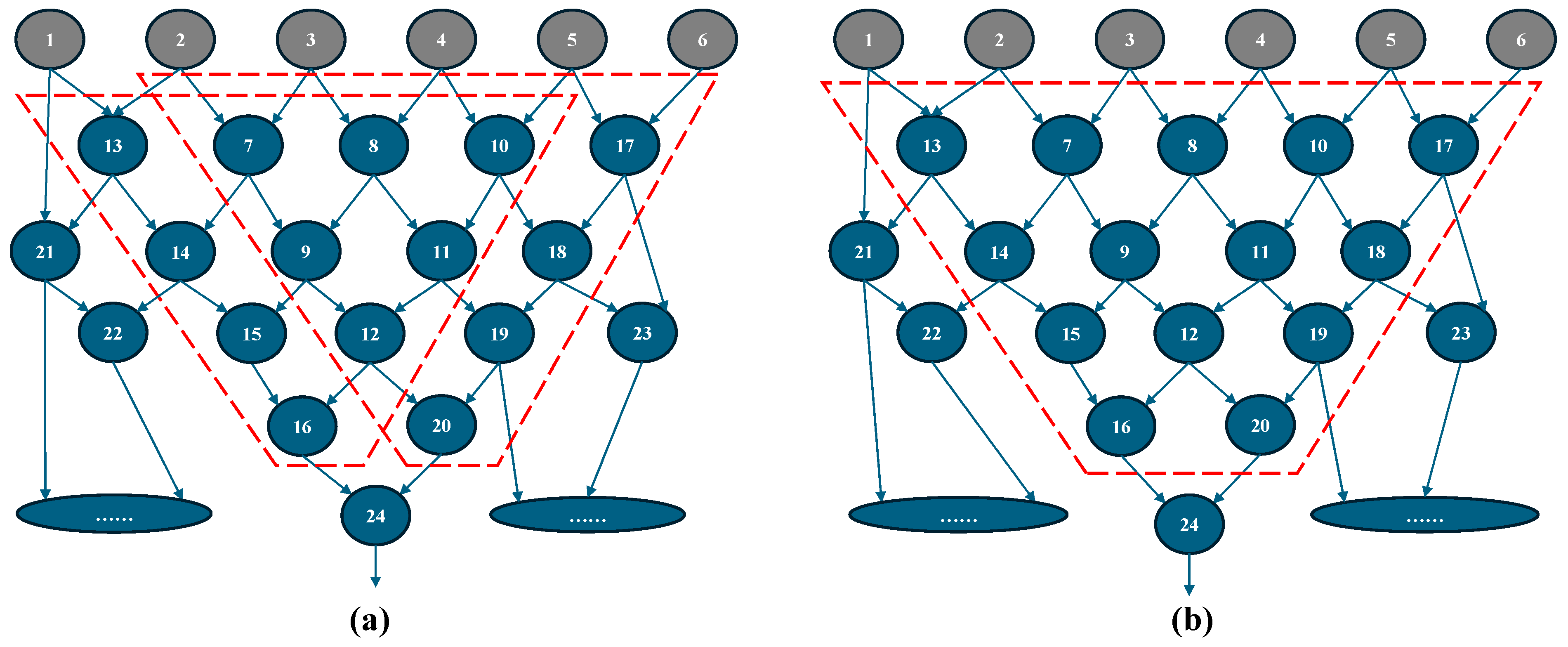
A field-programmable gate array (FPGA) is a reconfigurable circuit system that can implement various circuit functions using an array of configurable logic blocks (CLBs). Compared to application-specific integrated circuits (ASICs), FPGAs reduce initial development costs, and when compared to central processing units (CPUs), they offer better performance, making them widely used in both industry and academia. Traditional FPGAs consist of basic computing units known as single-output look-up tables (LUTs), where the LUT, the output flip-flop (FF), and the multiplexer (MUX) form a basic logic element (BLE), and multiple BLEs constitute a CLB [1,2], as shown in Figure 1 [3]. However, in practice, when a circuit is mapped to a LUT by logic synthesis tools (e.g., ABC), some LUTs may have fewer inputs than expected. For instance, in a six-input LUT system, some mapped LUTs may occupy only three inputs, leading to inefficient resource utilization of physical six-input LUTs. As illustrated by the simplified circuit directed acyclic graph (DAG) in Figure 2, Figure 2a presents the mapping result under a six-input, single-output scheme. Here, the network is an AIG (And-Inverter Graph), where each node in the graph represents an AND gate [4,5,6]. However, if the fanout number and LUT can be extended to a dual-output configuration, as shown in Figure 2b, the two single-output LUTs can be merged into a single dual-output LUT, reducing the area without degrading the delay.
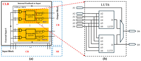
Figure 1.
(a) Generic FPGA architecture with fracturable LUTs and (b) detailed structure of example LUT from Xilinx UltraScale+ series [3].
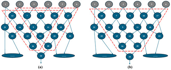
Figure 2.
An example of mapping results under six-input (a) single- and (b) dual-output LUT schemes. Here, the network is an AIG, where each node in the graph represents an AND gate.
To address this issue, both industry and academia have proposed various methods for improvement. For example, Xilinx’s Ultrascale+ series can fracture a six-input LUT into two five-input, single-output LUTs [3], while Intel’s Stratix series can decompose an eight-input LUT into several smaller LUTs with fewer than seven inputs [7]. Similarly, the VTR FPGA simulation platform provides architecture files that allow large LUTs to be split into multiple smaller LUTs [8], which enhances logic resource utilization and reduces the circuit area. Additionally, several studies have pointed out that emerging multi-output reconfigurable logic units may provide potential performance improvements compared to traditional LUTs [9,10,11,12], leading to more application possibilities for multi-output mapping techniques.
In academia, the ABC tool is commonly used to map circuits to LUTs [13], providing an efficient and fast single-output LUT mapping based on graph theory. Based on this platform, some works have attempted to implement multi-output LUT generation at the technology mapping level, replacing the simple merging of smaller-input LUTs. Jang et al. proposed a method called Mapping with Structural Choices (MSCs), combined with WireMap, a heuristic metrics-based approach, to merge small-sized LUTs into a single dual-output LUT [14]. This technique achieves less than 10% LUT number reductions. To enhance LUT area savings, Wang et al. proposed a double-output cut enumeration process based on the ABC single-output cut enumeration process, optimizing parameter selection and achieving significant area savings [15]. However, this method highly relies on the parameters during the dual-output cut generation, and a larger priority cut number is required for certain benchmark circuits, which increases time complexity and computational cost. Similar methods have also proposed to enhance the mapping efficiency of multi-output LUTs [16,17,18,19,20].
In this paper, we propose an efficient multi-output LUT generation method based on the interconnection relationships between LUTs. Specifically, we perform side-fanout insertion on each LUT at each layer based on the ABC single-output mapping result to cover the leaves of the next layer with the minimum number of LUTs, while merging smaller input LUTs within the same layer. Then, we perform LUT expansion on the remaining single-output LUTs layer by layer, transforming them into multi-output LUTs to further reduce the number of LUTs. The proposed mapping technique is universally applicable and can handle larger-scale circuits with better LUT area saving.
The main contributions of this paper are as follows:
- We propose an efficient multi-output LUT generation method, which includes a side-fanout insertion algorithm and a runtime multi-output LUT expansion algorithm.
- We propose a bottom-up layer-based cut merging and reduction method, which can efficiently utilize the features of multi-output cuts without worsening the delay.
- We develop a comprehensive FPGA design framework with the proposed mapping algorithm to demonstrate the potential advantages in terms of area, delay, and energy at the system level.
The rest of the paper is organized as follows: In Section 2, we introduce the proposed multi-output mapping technique, which includes side-fanout insertion, runtime multi-output LUT expansion, and a LUT merging and covering algorithm to improve mapping efficiency. Section 3 describes the experimental setup, including details of the benchmark netlists, FPGA architecture specifications, and simulation environment. Section 4 presents a detailed analysis of the results, with comparisons between our proposed technique and state-of-the-art approaches. Section 5 and Section 6 discuss a comparison of the proposed work with state-of-the-art methods and conclude with suggestions for future research.
2. Proposed Methods
In academic research, ABC is widely used for high-quality and efficient logic synthesis and FPGA LUT technology mapping [13]. In this section, building upon the ABC framework, we first introduce the fundamental concept of the cut-based LUT generation flow, followed by the proposed multi-output LUT mapping flow. This includes the side-fanout insertion and multi-output cut generation methods and algorithms, which emphasize interconnection-level high-quality multi-output cut generation. The overall flow of the proposed approach is depicted in Figure 3, with each step of the process discussed in detail in the following sections.
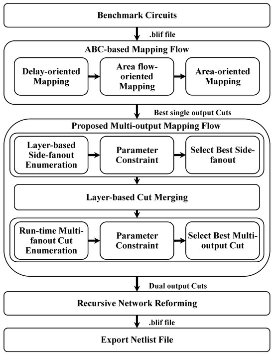
Figure 3.
Overview of the proposed multi-output mapping technique.
2.1. Single-Output Cut Enumeration
The standard approach to computing K-feasible cuts in an AIG follows a systematic pass from Primary Inputs (PIs) to Primary Outputs (POs). The cut set for an AND node is derived by merging the cut sets of its children, incorporating the trivial cut. A cut is considered K-feasible if it contains no more than K leaves and is dominated if another cut at the same root subsumes its coverage [4,5,6]. In a K-bounded subject graph, K-feasible cuts for all nodes are enumerated in an interconnection order to ensure that fanin cuts are available when computing the root’s cut set.
Defining as the K-feasible cut set of the node n, the operator is defined as follows:
Then, the cut set of node n can be computed by combining the cut sets of its fanin nodes as follows:
Here, and are the fanin nodes of node n. Using this formula, we can generate the cut set for all nodes in the AIG network, progressing from PIs to POs. By selecting the optimal cut for each node based on factors, such as delay, area, and power, we can construct a mapped LUT network through a recursive process that reforms the structure from POs back to PIs, following the reverse direction of cut generation.
2.2. Cut Interconnection-Based Multi-Output LUT Generation
As introduced in the background section, multi-output LUTs can merge smaller single-output LUTs to enhance resource utilization efficiency. In this section, we present a methodology for generating multi-output LUTs based on the interconnection of single-output cuts. We propose two algorithms—the side-fanout insertion algorithm and the runtime multi-output cut generation algorithm—designed to effectively reduce the number of LUTs while maintaining delay performance.
2.2.1. Side-Fanout Insertion Algorithm
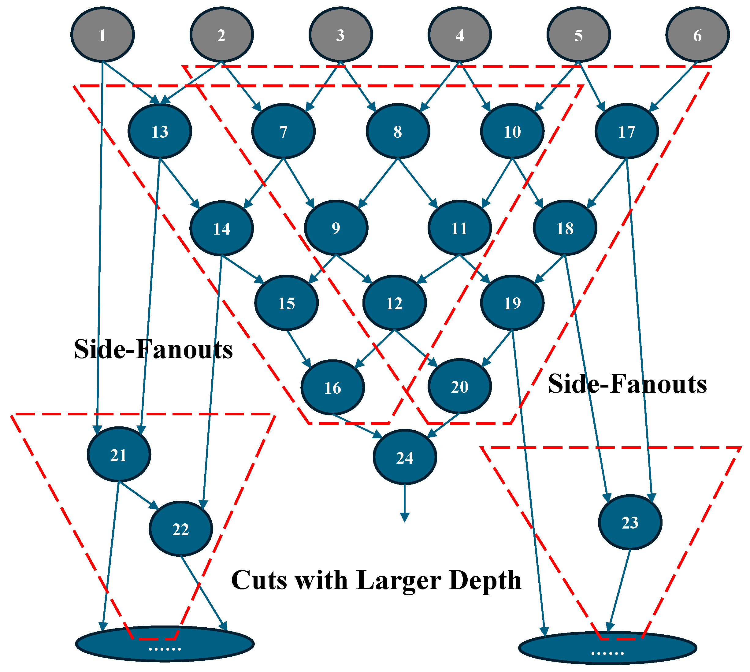
In the traditional single-output cut scheme, the cut structure resembles an inverted triangle, where all signals from the leaves propagate exclusively to the bottom output, which results in repeated nodes across different cuts. While this enumeration method is fast and efficient, it overlooks critical side-node interconnections that could be leveraged by multi-output cuts. As illustrated in Figure 4, side-fanouts of a single-output cut can serve as inputs for cuts in the next layer. By allowing a multi-output cut to designate these side-fanouts as additional outputs, the number of LUTs can be reduced during the recursive network reformation process from POs to PIs.
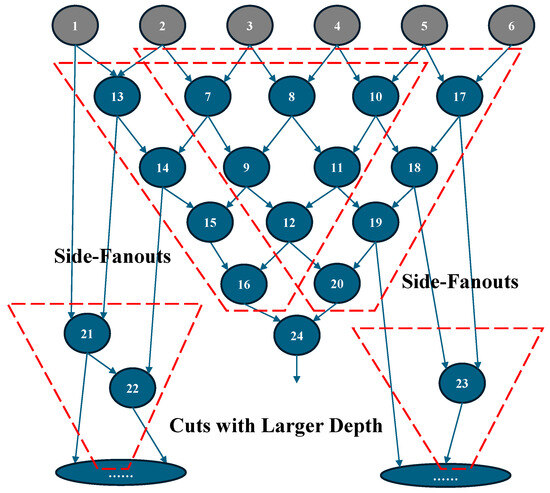
Figure 4.
An example illustrating the potential application of side-fanouts and the generation of multi-output cuts.
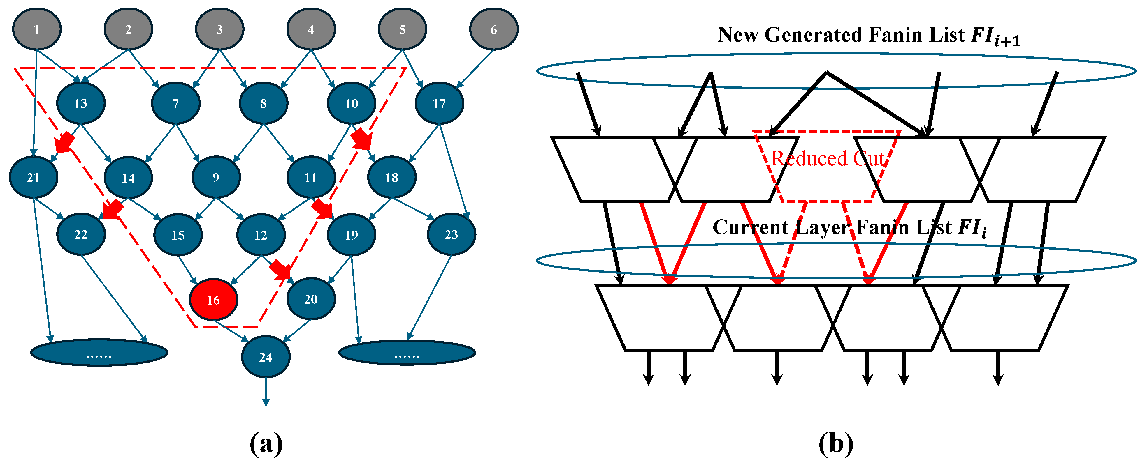
In detail, we define the fanins of cuts at the same level as , as shown in Figure 5b. For each single cut generated by ABC mapping, side-fanouts are considered for inclusion. Specifically, for a given cut that provides signals for , all possible side-fanouts are enumerated. Among these candidates, the side-fanout with the highest coverage of is selected as the second output of the cut. Once selected, is updated by removing the covered fanins, and this process continues iteratively until all nodes in are covered. During the covering process, there is a high probability that the total number of cuts incorporating a second fanout is lower than that of the original single-output cuts, as indicated by the red-dashed block in Figure 5b. This reduction directly contributes to decreasing the overall number of LUTs. Afterward, the next-level fanins, , are generated based on the newly formed cut layer. We implement this process using a recursive loop, ensuring that the iteration continues until contains only PIs. The pseudocode for this process is presented in Algorithm 1.
| Algorithm 1 Side-fanout Insertion Algorithm | ||||
| Require: Layer leaves from POs to PIs | ||||
| Ensure: Insert side-fanout and generation of the next layer’s leaves | ||||
| 1: | function SideFanoutInsertion(layer_leaves) | |||
| 2: | Step 1: Enumerate possible side-fanouts | |||
| 3: | for each node in leaves do | |||
| 4: | cut_fanout_list = FindSideFanouts(current_node_cut) | |||
| 5: | end for | |||
| 6: | Step 2: Leaves coverage and cuts reduction | |||
| 7: | while exist layer_leaves not visited do | |||
| 8: | best_node: cut with most coverage with optimized side-fanout | |||
| 9: | for each fanout_node in best_node cut do | |||
| 10: | mark fanout_node as visited | |||
| 11: | end for | |||
| 12: | end while | |||
| 13: | Step 3: Generate the next layer’s leaves | |||
| 14: | Initialize layer_leaves_next as empty | |||
| 15: | for each selected node in leaves do | |||
| 16: | Add current_cut leaves to layer_leaves_next | |||
| 17: | end for | |||
| 18: | Step 4: Recursive loop | |||
| 19: | if layer_leaves_next is not empty then | |||
| 20: | SideFanoutInsertion(layer_leaves_next) | |||
| 21: | end if | |||
| 22: | end function | |||

Figure 5.
Layer-based side-fanout insertion and LUT reduction. (a) Enumeration of possible side-fanouts of a single-output cut; (b) merging and reduction of same layer cuts.
Meanwhile, within the same layer of cuts, multiple cuts exist with identical input net nodes. These cuts can be merged into a single dual-output LUT if the total number of inputs, , does not exceed . Thus, following the side-fanout insertion and coverage process, a layer-based cut merging procedure is executed to efficiently combine cuts with the same input pins. This approach not only reduces the number of LUTs but also improves system-level placement and routing considerations in FPGA implementation. Since cuts with identical inputs are merged, they tend to remain physically close, thereby enhancing spatial locality. In terms of C language implementation, this process is analogous to side-fanout insertion but is significantly simpler. A nested for loop can be employed to traverse the cuts within the same layer and perform the merging operation effectively.
2.2.2. Runtime Multi-Output LUT Expansion Algorithm
The side-fanout insertion and same-layer cut merging processes reduce the number of cuts based on the single-output cuts initially generated by ABC. In this section, we aim to expand the remaining unchanged single-output cuts after the previous processes. The key concept of this approach is to actively generate multi-output cuts, allowing multiple roots within the same cut. This process consists of two main components. The first component involves generating multi-output cuts using an optimized Breadth-First Search (BFS) recursive algorithm [21], which efficiently explores potential multi-output cuts for a given root. The second component is a layer-based coverage and merging procedure, similar to the side-fanout insertion algorithm.
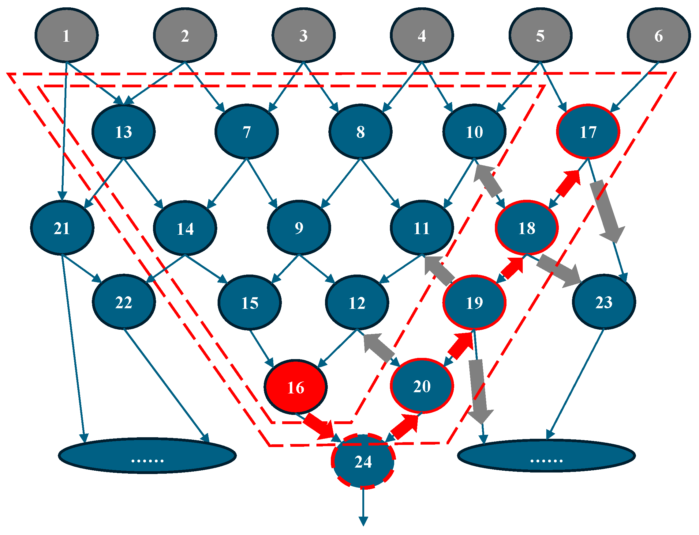
As shown in Figure 6, the target root node is highlighted in red with an index of 16. The search algorithm first explores the fanout nodes of node 16, leading to the exploration of node 24. However, node 24 is not added to the cut because only nodes with a level that is not larger than the current root node’s level are considered, ensuring compatibility with the layer-based analysis scheme.
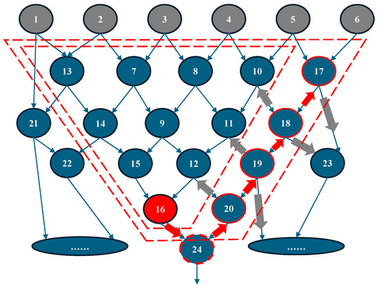
Figure 6.
An example of the BFS-based multi-output cut generation algorithm. The red arrow represents successfully explored nodes, whereas the dark nodes indicate failed attempts—either because the node already exists in the current cut or because adding it would exceed the I/O number limit.
For the explored nodes with a level greater than the root node, only their fanin nodes are further searched. In this case, node 20 is added to the cut because it shares the same level as node 16, and the I/O count of the expanded cut does not exceed the predefined limit (6 inputs, 2 outputs). Next, nodes 12 and 19 are explored. Since node 20 has only one fanout, node 24, which has already been visited, only fanins of node 20 are further explored. For nodes with the same level as the root node, as well as those with a lower level, both their fanins and fanouts are explored. This process continues iteratively until there are no more candidate nodes to explore or the I/O size of the cut exceeds the predefined limit. The pseudocode for multi-output cut generation is presented in Algorithm 2.
| Algorithm 2 Recursive Cut Expansion Algorithm | ||||||
| Require: Logic network represented as a set of nodes and cuts | ||||||
| Ensure: Recursive expansion of cuts satisfy fanin/fanout/level constraints | ||||||
| 1: | Declare Constraints: fanin/fanout/level/max enumeration number | |||||
| 2: | function ExpandCut(current_node, level, current_cut) | |||||
| 3: | if current_node is not visited then | |||||
| 4: | Mark current_node as visited | |||||
| 5: | if satisfy Constraints then | |||||
| 6: | if NotRepeated(current_cut, cut_list) then | |||||
| 7: | Add current_cut to cut_list | |||||
| 8: | end if | |||||
| 9: | if curr_node.Level <= root_level then | |||||
| 10: | for each fanout node do | |||||
| 11: | current_cut add fanout_node | |||||
| 12: | ExpandCut(fanout_node, new_level, current_cut) | |||||
| 13: | end for | |||||
| 14: | for each fanin node do | |||||
| 15: | current_cut add fanin_node | |||||
| 16: | ExpandCut(fanin_node, new_level, current_cut) | |||||
| 17: | end for | |||||
| 18: | else | |||||
| 19: | for each fanin node do | |||||
| 20: | current_cut add fanin_node | |||||
| 21: | ExpandCut(fanin_node, new_level, current_cut) | |||||
| 22: | end for | |||||
| 23: | end if | |||||
| 24: | else | |||||
| 25: | Remove current_node from current_cut | |||||
| 26: | end if | |||||
| 27: | Add current_cut to cut_list | |||||
| 28: | end if | |||||
| 29: | end function | |||||
The remaining part of the runtime multi-output LUT expansion algorithm is similar to the side-fanout insertion process, as both rely on a bottom-up recursive, layer-based cut merging and reduction strategy. A critical requirement for multi-output selection is that the chosen multi-output cut must minimize key parameters, such as area, delay, and edge count. Based on practical experiments, we adopt an area calculation method similar to ABC’s exact area flow. This approach ensures that the area of each multi-output cut is accurately evaluated, guaranteeing that cut expansion does not degrade the area efficiency compared to the original single-output cuts. The pseudocode for this process is presented in Algorithm 3.
| Algorithm 3 Runtime Multi-output Cut Expanding Algorithm | ||||
| Require: Layer leaves (initial nodes for expansion) | ||||
| Ensure: Recursive expansion of cuts and generation of the next layer’s leaves | ||||
| 1: | function RunTimeExpand(layer_leaves) | |||
| 2: | Step 1: Recursive expansion based on ExpandCut | |||
| 3: | for each node in leaves do | |||
| 4: | Initialize current_cut = ABC_Best(current_node) | |||
| 5: | cut_list = ExpandCut(current_node, level, current_cut) | |||
| 6: | BestMultiCut = BestMultiCutSel(cut_list, leaves) | |||
| 7: | Assign BestMultiCut to current_node | |||
| 8: | end for | |||
| 9: | Step 2: Leaves coverage and cuts reduction | |||
| 10: | while exist leaves not visited do | |||
| 11: | best_node = CutWithMaxCoverage(leaves_unvisited) | |||
| 12: | for each fanout_node in best_node cut do | |||
| 13: | mark fanout_node as visited | |||
| 14: | end for | |||
| 15: | end while | |||
| 16: | Step 3: Generate the next layer’s leaves | |||
| 17: | Initialize layer_leaves_next as empty | |||
| 18: | for each selected node in leaves do | |||
| 19: | Add current_cut leaves to layer_leaves_next | |||
| 20: | end for | |||
| 21: | Step 4: Recursive loop | |||
| 22: | if layer_leaves_next is not empty then | |||
| 23: | RunTimeExpand(layer_leaves_next) | |||
| 24: | end if | |||
| 25: | end function | |||
| 26: | ||||
| 27: | function BestMultiCutSel(cut_list, leaves) | |||
| 28: | Goal: Ensure the selected multi-output cut has the smallest area | |||
| 29: | for each cut in cut_list do | |||
| 30: | cut_area = AreaCountRec(current_node) | |||
| 31: | end for | |||
| 32: | Cut_best = cut_with_minArea | |||
| 33: | end function | |||
3. Experimental Configurations and Settings
This work is based on the well-known open-source synthesis tool, ABC, which can be found in [22]. ABC is developed in the C programming language and provides various functions for FPGA mapping. Our dual-fanout FPGA mapping method is implemented within this framework.
To evaluate our proposed mapping technique against existing works, we adopt the same FPGA architectures as referenced in [15], specifically Xilinx’s Ultrascale+ and Versal series. The primary distinction between these two architectures lies in their LUT designs, which affect both the maximum number of unique inputs and the maximum number of shared inputs between fractured LUTs. The detailed specifications of these architectures are provided in Table 1, which is consistent with the reference work to ensure a fair comparison. While some parameters may differ slightly from the official Xilinx datasheets [3,23], this alignment maintains consistency in benchmarking and evaluation.

Table 1.
Parameters of two typical FPGA series.
Additionally, we utilize the full-list EPFL benchmark suite [24], which includes large-scale circuits with up to 200,000 AIG nodes. To ensure a fair comparison with the reference work [15], we adopt two mapping strategies: (1) optimized benchmarks, where circuits are pre-processed using the ABC commands “resyn; resyn2” to refine the circuit structure, as done in the reference work, and (2) original benchmarks, where circuits are used in their unmodified form. These strategies allow for an equitable evaluation of our mapping technique against state-of-the-art methods while demonstrating its universal applicability to any combinational circuit. The detailed benchmark netlist information is provided in Table 2. In the results section, we will present mapping results from three different mapping techniques: (1) the ABC-based single-output LUT as the baseline, (2) the dual-output mapping result from the reference work, and (3) our proposed multi-output mapping technique.
Table 2.
Benchmark netlist information.
Considering that the final performance of a circuit mapped to an FPGA is not solely determined by the LUT mapping phase, but is also significantly influenced by system-level placement and routing, it is essential to verify that the mapping results are compatible with the subsequent placement and routing stages. In other words, we need to ensure that the multi-output LUT maintains its advantages after placement and routing. To address this, we conduct system-level simulations using the open-source FPGA simulation tool VTR [1,2,8], which is widely used in academic research. For simplicity, we modeled the Xilinx FPGA architecture by fixing the number of BLEs per CLB. The detailed architecture-level parameters are provided in Table 3. Here, and are parameters that reflect the flexibility of the connection block, while reflects the flexibility of the switch box. More details on these parameters can be found in [1]. For the switching energy calculation, the activity file is generated by ACE2.0 [25], which generates the effective activity factors for each connection in an FPGA system based on the circuit netlist generated by ABC. The interconnect capacitance and resistance per unit length of copper wires are calculated based on the following existing works [26,27].
Table 3.
Parameter setting for VTR FPGA system-level simulation.
The program runs on a desktop with an Intel i9-9900 CPU and 32 GB RAM. The program does not have specific requirements for the CPU, and it should be compatible with most modern processors. Based on our tests, the code requires no more than 16 GB of memory, even for the largest benchmark netlists. Therefore, it should be applicable to most mainstream personal computers.
4. Simulation Results
4.1. Comparison Between Different FPGA Architectures
As shown in Figure 7a, both the UltraScale+ and Versal dual-output architectures achieve significant area savings compared to the single-output architecture, with area reductions of up to 33.9% and 21.3%, respectively. Figure 7b illustrates that the Versal architecture exhibits a higher ratio of dual-output LUTs, with up to 59% of the mapped LUTs being dual-output, while this figure for the UltraScale+ architecture is 32%. The Versal architecture benefits more from dual-output LUTs than the UltraScale+ due to key differences in their flexibility. As shown in Table 1, the Versal architecture allows a LUT to be split into two sub-LUTs with up to six shared inputs, while the UltraScale+ architecture only supports a maximum of five shared inputs when a LUT is split. This additional flexibility in the Versal architecture enables more efficient utilization of dual-output LUTs, leading to improved mapping outcomes. The results demonstrate that architectures with a higher percentage of dual-output LUTs achieve greater area savings, confirming that dual-output LUTs effectively optimize the circuit area. The benchmark used for these results is the original EPFL benchmark list.
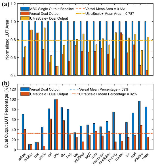
Figure 7.
Comparison between different FPGA architectures. (a) Comparison of the number of LUTs among FPGAs using single-output LUTs, Versal architecture, and UltraScale+ architecture, where area is normalized by single-output LUT baseline. (b) Percentage of dual-output LUTs for different architectures.
4.2. Comparison with State-of-the-Art Dual-Output Mapping Technique
As shown in Table 4, we compare the mapping results with the work from [15]. All benchmarks are processed using the “resyn; resyn2” command as a preprocessing step to ensure a fair comparison. It should be noted that Table 4 only includes the 13 benchmarks used in the reference work, with the full set of results available in Appendix A. The results demonstrate that the proposed mapping technique achieves up to 35% and 6% averaged area savings, compared to the state-of-the-art ABC six-input, single-output LUT mapping technique and previous work focusing on dual-output LUT mapping techniques that optimize cut generation parameters.
Table 4.
Comparison with state-of-the-art dual-output mapping technique.
In a detailed comparison between the reference work and our proposed method, three netlists—“adder”, “arbiter” and “dec”—exhibit slightly greater area savings in the reference work when implemented on the Versal architecture. These few netlists feature relatively regular and well-structured hierarchical designs, making the parameter-based mapping technique is more efficient. However, for larger-scale netlists with more structurally random characteristics, the proposed method demonstrates a significant advantage. This further validates that the cut interconnection-based multi-output mapping technique is more universally applicable. In addition, for some small-sized netlists, such as “int2float”, “cavlc”, and “ctrl”, the netlist sizes are relatively small, resulting in a similar LUT area utilization for both the reference work and the proposed method.
4.3. Runtime Analysis
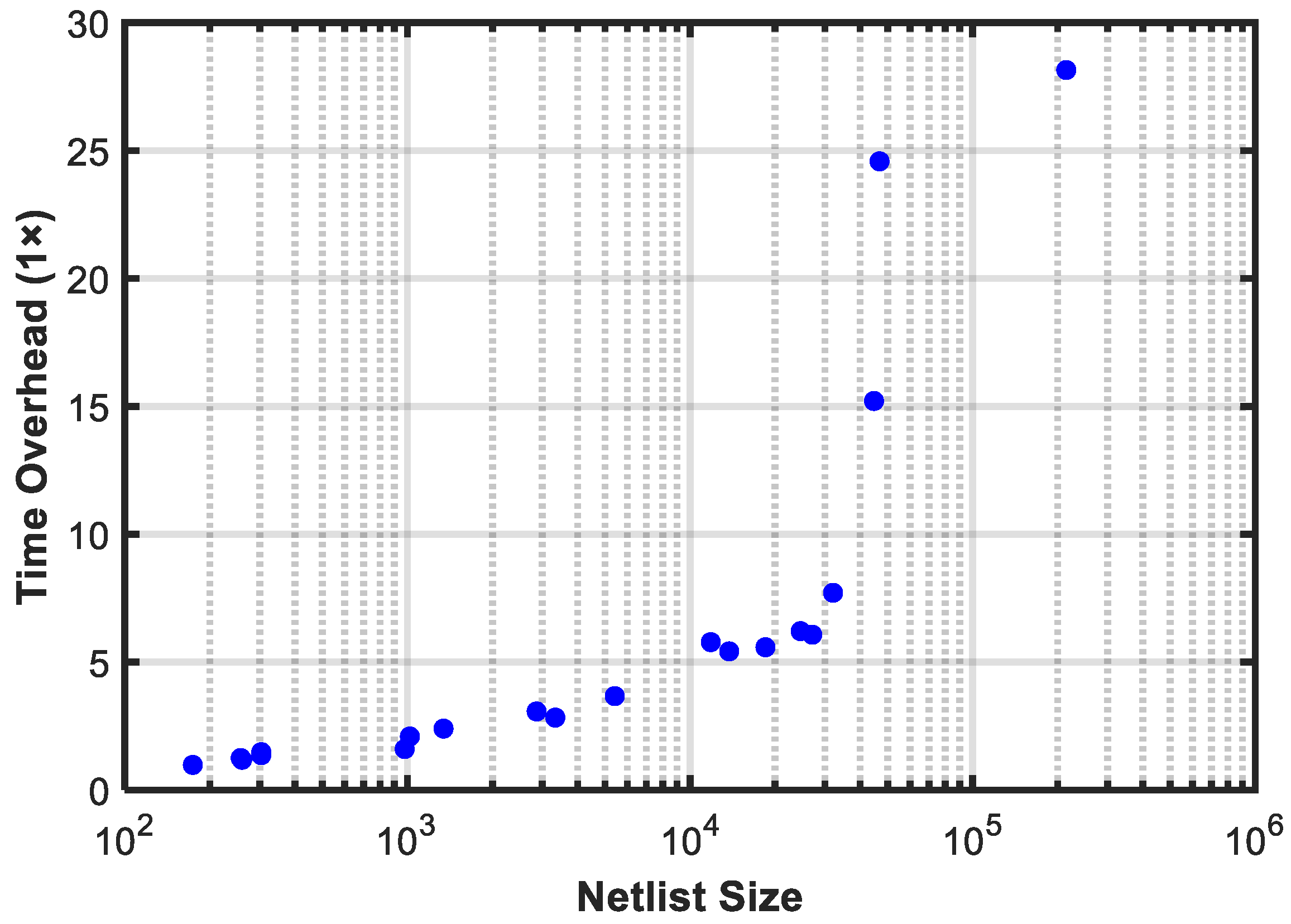
As shown in Table 5, although the proposed mapping method demonstrates higher dual-output mapping efficiency, the trade-off is an increased execution time compared to the ABC single-output mapping. The time overhead is minimal when the input netlist size is small; however, as the netlist size increases, more significant time overhead is observed. As depicted in Figure 8, this is due to the linear time complexity of the proposed method at the code realization level. Future work, such as algorithm optimization, will be explored to address and reduce this time overhead.
Table 5.
Program execution time for ABC and proposed mapping method with Ultrascale+.

Figure 8.
Relationship between program execution time overhead and netlist size (AIG node number).
4.4. FPGA System-Level Simulation Results
As shown in Table 6, both dual-output LUT architectures maintain an advantage in most parameters. Specifically, for the Versal series architecture, up to 13.92% area savings, 11.51% delay reductions, 7.31% wirelength savings, and 8.41% switching energy savings can be achieved compared to the single-output LUT baseline. However, for certain netlists, such as “priority”, dual-output LUT architectures exhibit a higher delay, and for “arbiter”, they show an increased wirelength. These “abnormal” results suggest that system-level factors related to FPGA placement and routing should be considered, even though dual-output LUT architectures already provide area advantages after technology mapping [28,29,30]. For example, although dual-output LUTs offer higher mapping efficiency, leading to a reduction in the LUT area, a larger number of input/output net nodes can increase placement and routing congestion, ultimately resulting in a longer wirelength. Therefore, future work will focus on optimizing the integration of LUT technology mapping with system-level placement and routing to mitigate these challenges.
Table 6.
VTR-based FPGA system level simulation results.
5. Discussion
The simulation results demonstrate that the proposed dual-output mapping technique achieves significant improvements over existing approaches. Specifically, compared to state-of-the-art ABC single-output mapping, our method reduces the LUT area by up to 35%. When compared to existing dual-output mapping techniques, our approach still delivers notable area savings of up to 6%.
Both our proposed work and the referenced work are based on the ABC synthesis platform and aim to optimize the mapping flow for dual-output LUTs. The key difference lies in the method of dual-output cut generation. The referenced work employs a k-input, l-output cut-based approach, which directly enumerates potential dual-output cuts during the enumeration phase. While effective in certain scenarios, this method requires exploring many possible cuts, making it memory-intensive and time-consuming, and thus less suitable for large or complex benchmark netlists.
In contrast, our proposed method takes an interconnection-oriented perspective. Instead of directly enumerating dual-output cuts, we focus on merging and combining highly related single-output cuts that are generated by the standard ABC mapping flow. This reformulates the dual-cut generation problem as a mathematical covering and merging problem, which significantly simplifies the process. As a result, our method is more scalable and broadly applicable across a wide range of benchmark circuits, providing a practical and efficient alternative to exhaustive enumeration.
However, in terms of runtime, there is a noticeable time overhead compared to the ABC single-output mapping flow. This is primarily due to the inclusion of repeated executions, such as checking the flow of the layer-based cut merging, which involves identifying common nodes between two cuts. These steps can be further optimized at the code realization level. When compared to the state-of-the-art dual-output method in the referenced work, which incurs a 3.5× time overhead, our proposed method achieves a smaller time overhead of 2.8× with the same benchmark netlists. Reducing runtime during the mapping process is a critical aspect, and optimization efforts in this area will be addressed in future work.
6. Conclusions
In this work, we propose a cut interconnection-based multi-output LUT mapping technique that effectively utilizes the interconnection information of single-output cuts to enable efficient dual-output mapping. The approach integrates several key algorithmic components, including side-fanout insertion, runtime multi-output LUT expansion, and a LUT merging and covering algorithm, all designed to enhance the overall mapping quality and reduce area usage.
We evaluate the proposed method using the complete set of EPFL benchmark circuits. The experimental results show that our technique achieves significant improvements over existing approaches. Specifically, compared to the state-of-the-art ABC single-output mapping, our method reduces the LUT area by up to 35%. When compared to existing dual-output mapping techniques, our approach still delivers notable area savings of up to 6%. However, in terms of code execution time, the trade-off involves an increased execution duration compared to the ABC single-output mapping. While the time overhead remains minimal for smaller input netlists, it becomes more pronounced as the netlist size grows. This is attributable to the linear time complexity of the proposed method at the code realization level. Future work will focus on reducing the time complexity at the code level and extending the approach to support other emerging multi-output logic units.
Author Contributions
Algorithm development, simulation, and manuscript preparation were conducted by S.L., L.S. and Q.Q. Paper writing guidance was provided by Q.L. and S.J. Project administration and supervision were carried out by C.P. All authors have read and agreed to the published version of the manuscript.
Funding
This work is funded by the Advanced Scientific Computing Research (ASCR) program of the Department of Energy (DoE) through the award DE-SC0022881, imec, and National Science Foundation (NSF) under grant CCF-2219753.
Data Availability Statement
All the data and code can be downloaded from GitHub with the following link: https://github.com/Sheng1994/abcpercy_merge.git (accessed on 26 April 2025). Please email the corresponding author for download permission.
Conflicts of Interest
The authors declare no conflicts of interest.
Abbreviations
The following abbreviations are used in this manuscript:
| FPGA | Field-Programmable Gate Array |
| CPU | Central Processing Unit |
| ASIC | Application-Specific Integrated Circuit |
| LUT | Look-Up Table |
| BLE | Basic Logic Element |
| CLB | Configurable Logic Blocks |
| FF | Flip-Flop |
| DAG | Directed Acyclic Graph |
| AIG | And Inverter Graph |
| PIs | Primary Inputs |
| POs | Primary Outputs |
Appendix A
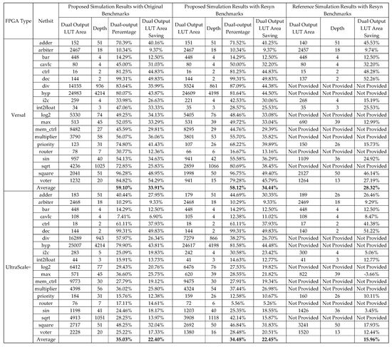
Figure A1.
Full simulation results.
Figure A1.
Full simulation results.

References
- Betz, V.; Rose, J.; Marquardt, A. Architecture and CAD for Deep-Submicron FPGAs; Springer Science & Business Media: Berlin/Heidelberg, Germany, 2012; Volume 497. [Google Scholar]
- Ahmed, E.; Rose, J. The effect of LUT and cluster size on deep-submicron FPGA performance and density. In Proceedings of the 2000 ACM/SIGDA Eighth International Symposium on Field Programmable Gate Arrays, Monterey, CA, USA, 10–11 February 2000; pp. 3–12. [Google Scholar]
- AMD. Vivado UltraScale Libraries User Guide (UG974)—LUT6; AMD: Santa Clara, CA, USA, 2024. [Google Scholar]
- Cong, J.; Liu, B.; Neuendorffer, S.; Noguera, J.; Vissers, K.; Zhang, Z. High-level synthesis for FPGAs: From prototyping to deployment. IEEE Trans. Comput.-Aided Des. Integr. Circuits Syst. 2011, 30, 473–491. [Google Scholar] [CrossRef]
- Cong, J.; Ding, Y. FlowMap: An optimal technology mapping algorithm for delay optimization in lookup-table based FPGA designs. IEEE Trans. Comput.-Aided Des. Integr. Circuits Syst. 1994, 13, 1–12. [Google Scholar] [CrossRef]
- Mishchenko, A.; Chatterjee, S.; Brayton, R. Improvements to technology mapping for LUT-based FPGAs. In Proceedings of the 2006 ACM/SIGDA 14th International Symposium on Field Programmable Gate Arrays, Monterey, CA, USA, 22–24 February 2006; pp. 41–49. [Google Scholar]
- Intel Stratix FPGA. Available online: https://www.intel.com/content/www/us/en/products/details/fpga/stratix.html (accessed on 21 March 2025).
- Murray, K.E.; Petelin, O.; Zhong, S.; Wang, J.M.; Eldafrawy, M.; Legault, J.-P.; Sha, E.; Graham, A.G.; Wu, J.; Walker, M.J. VTR 8: High-performance CAD and customizable FPGA architecture modelling. ACM Trans. Reconfigurable Technol. Syst. 2020, 13, 9. [Google Scholar] [CrossRef]
- Shang, L.; Lu, S.; Zhang, Y.; Jung, S.; Pan, C. Directed Acyclic Graph-Based Datapath Synthesis Using Graph Isomorphism and Gate Reconfiguration. Chips 2024, 3, 182–195. [Google Scholar] [CrossRef]
- Shang, L.; Lu, S.; Jung, S.; Pan, C. Novel Fence Generation Methods for Accelerating Reconfigurable Exact Synthesis. In Proceedings of the 2023 IEEE 66th International Midwest Symposium on Circuits and Systems (MWSCAS), Tempe, AZ, USA, 6–9 August 2023; pp. 506–510. [Google Scholar]
- Lu, S.; Shang, L.; Jung, S.; Zhang, Y.; Pan, C. A Novel Delay-Aware Packing Algorithm for FPGA Architecture Using RFET. In Proceedings of the 2024 IEEE 67th International Midwest Symposium on Circuits and Systems (MWSCAS), Springfield, MA, USA, 11–14 August 2024; pp. 362–366. [Google Scholar]
- Gaillardon, P.-E.; Tang, X.; Kim, G.; De Micheli, G. A novel FPGA architecture based on ultrafine grain reconfigurable logic cells. IEEE Trans. Very Large Scale Integr. Syst. 2014, 23, 2187–2197. [Google Scholar] [CrossRef]
- Brayton, R.; Mishchenko, A. ABC: An academic industrial-strength verification tool. In Proceedings of the Computer Aided Verification: 22nd International Conference, CAV 2010, Edinburgh, UK, 15–19 July 2010; pp. 24–40. [Google Scholar]
- Jang, S.; Chan, B.; Chung, K.; Mishchenko, A. Wiremap: FPGA technology mapping for improved routability and enhanced LUT merging. ACM Trans. Reconfigurable Technol. Syst. 2009, 2, 14. [Google Scholar] [CrossRef]
- Wang, F.; Zhu, L.; Zhang, J.; Li, L.; Zhang, Y.; Luo, G. Dual-output LUT merging during FPGA technology mapping. In Proceedings of the 39th International Conference on Computer-Aided Design, San Diego, CA, USA, 2–5 November 2020; pp. 1–9. [Google Scholar]
- Calvino, A.T.; De Micheli, G. Technology mapping using multi-output library cells. In Proceedings of the 2023 IEEE/ACM International Conference on Computer Aided Design (ICCAD), San Francisco, CA, USA, 28 October–2 November 2023; pp. 1–9. [Google Scholar]
- Shi, J.; Wang, X.; Meng, C.; Qian, W. QUADOL: A Quality-Driven Approximate Logic Synthesis Method Exploiting Dual-Output LUTs for Modern FPGAs. arXiv 2024, arXiv:2411.18330. [Google Scholar]
- Jiang, Z.; Lin, C.Y.; Yang, L.; Wang, F.; Yang, H. Exploring architecture parameters for dual-output LUT based FPGAs. In Proceedings of the 2014 24th International Conference on Field Programmable Logic and Applications (FPL), Munich, Germany, 2–4 September 2014; pp. 1–6. [Google Scholar]
- Lee, J.-Y.; Hu, Y.; Majumdar, R.; He, L.; Li, M. Fault-tolerant resynthesis with dual-output LUTs. In Proceedings of the 2010 15th Asia and South Pacific Design Automation Conference (ASP-DAC), Taipei, Taiwan, 18–21 January 2010; pp. 325–330. [Google Scholar]
- Hu, Y.; Shih, V.; Majumdar, R.; He, L. FPGA area reduction by multi-output function based sequential resynthesis. In Proceedings of the 45th Annual Design Automation Conference, Anaheim, CA, USA, 8–13 June 2008; pp. 24–29. [Google Scholar]
- Beamer, S.; Asanović, K.; Patterson, D. Direction-optimizing breadth-first search. Sci. Program. 2013, 21, 137–148. [Google Scholar] [CrossRef]
- ABC: A System for Sequential Logic Synthesis and Verification. Available online: https://github.com/berkeley-abc/abc (accessed on 23 April 2025).
- AMD. Versal Adaptive SoC Configurable Logic Block Architecture Manual (AM005); AMD: Santa Clara, CA, USA, 2024. [Google Scholar]
- Amarú, L.; Gaillardon, P.-E.; De Micheli, G. The EPFL combinational benchmark suite. In Proceedings of the 24th International Workshop on Logic & Synthesis (IWLS), Mountain View, CA, USA, 12–13 June 2015. [Google Scholar]
- Lamoureux, J.; Wilton, S.J. Activity estimation for field-programmable gate arrays. In Proceedings of the 2006 International Conference on Field Programmable Logic and Applications, Madrid, Spain, 28–30 August 2006; pp. 1–8. [Google Scholar]
- Pan, C.; Naeemi, A. A proposal for a novel hybrid interconnect technology for the end of roadmap. IEEE Electron Device Lett. 2013, 35, 250–252. [Google Scholar] [CrossRef]
- Pan, C.; Naeemi, A. A paradigm shift in local interconnect technology design in the era of nanoscale multigate and gate-all-around devices. IEEE Electron Device Lett. 2015, 36, 274–276. [Google Scholar] [CrossRef]
- Elgammal, M.A.; Murray, K.E.; Betz, V. RLPlace: Using reinforcement learning and smart perturbations to optimize FPGA placement. IEEE Trans. Comput.-Aided Des. Integr. Circuits Syst. 2021, 41, 2532–2545. [Google Scholar] [CrossRef]
- Ababei, C.; Feng, Y.; Goplen, B.; Mogal, H.; Zhang, T.; Bazargan, K.; Sapatnekar, S. Placement and routing in 3D integrated circuits. IEEE Des. Test Comput. 2005, 22, 520–531. [Google Scholar] [CrossRef]
- Li, W.; Dhar, S.; Pan, D.Z. UTPlaceF: A routability-driven FPGA placer with physical and congestion aware packing. IEEE Trans. Comput.-Aided Des. Integr. Circuits Syst. 2017, 37, 869–882. [Google Scholar] [CrossRef]


Disclaimer/Publisher’s Note: The statements, opinions and data contained in all publications are solely those of the individual author(s) and contributor(s) and not of MDPI and/or the editor(s). MDPI and/or the editor(s) disclaim responsibility for any injury to people or property resulting from any ideas, methods, instructions or products referred to in the content. |
© 2025 by the authors. Licensee MDPI, Basel, Switzerland. This article is an open access article distributed under the terms and conditions of the Creative Commons Attribution (CC BY) license (https://creativecommons.org/licenses/by/4.0/).