
Graphene and Two-Dimensional Materials for Optoelectronic Applications


Abstract
:
1. Introduction
2. Technology of 2D Materials
3. Transparent Conductive Electrodes
4. Photodetectors
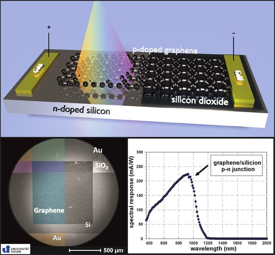
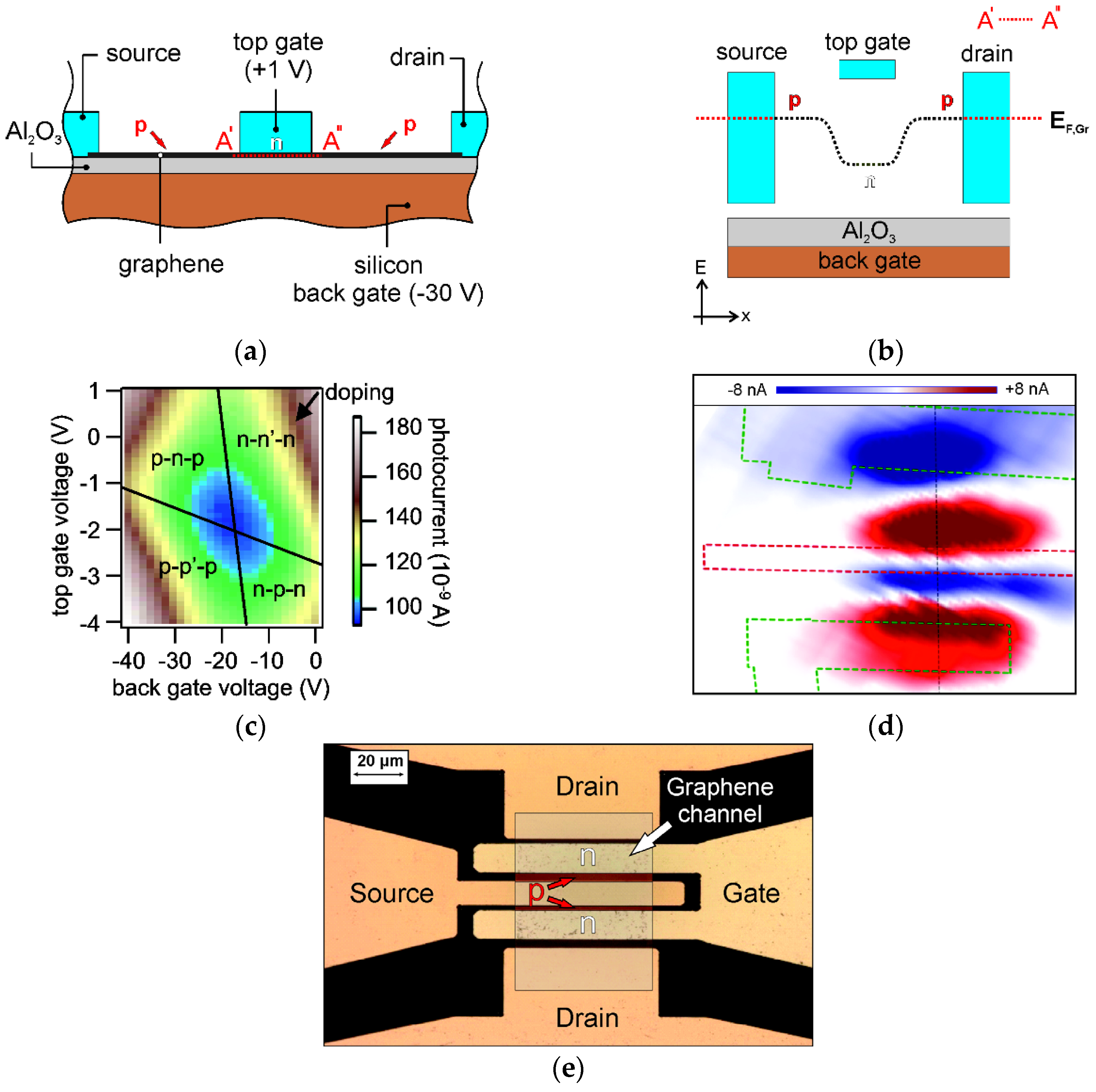
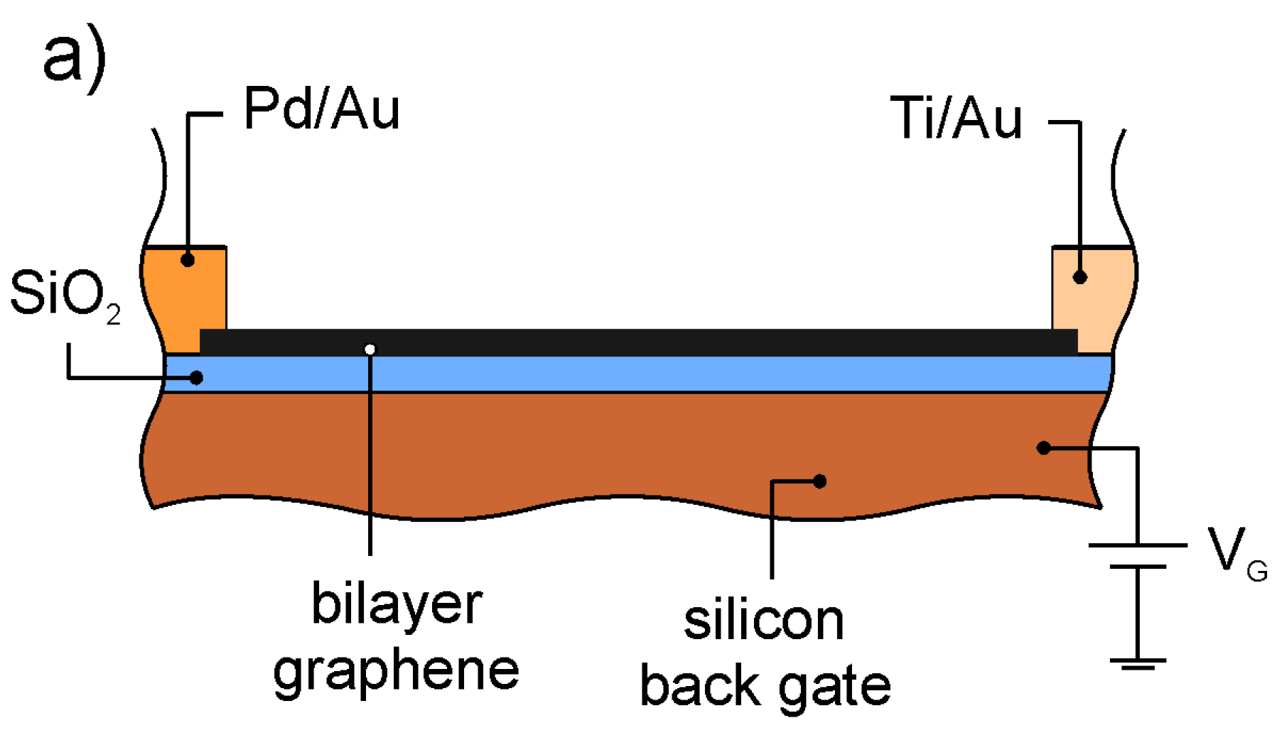
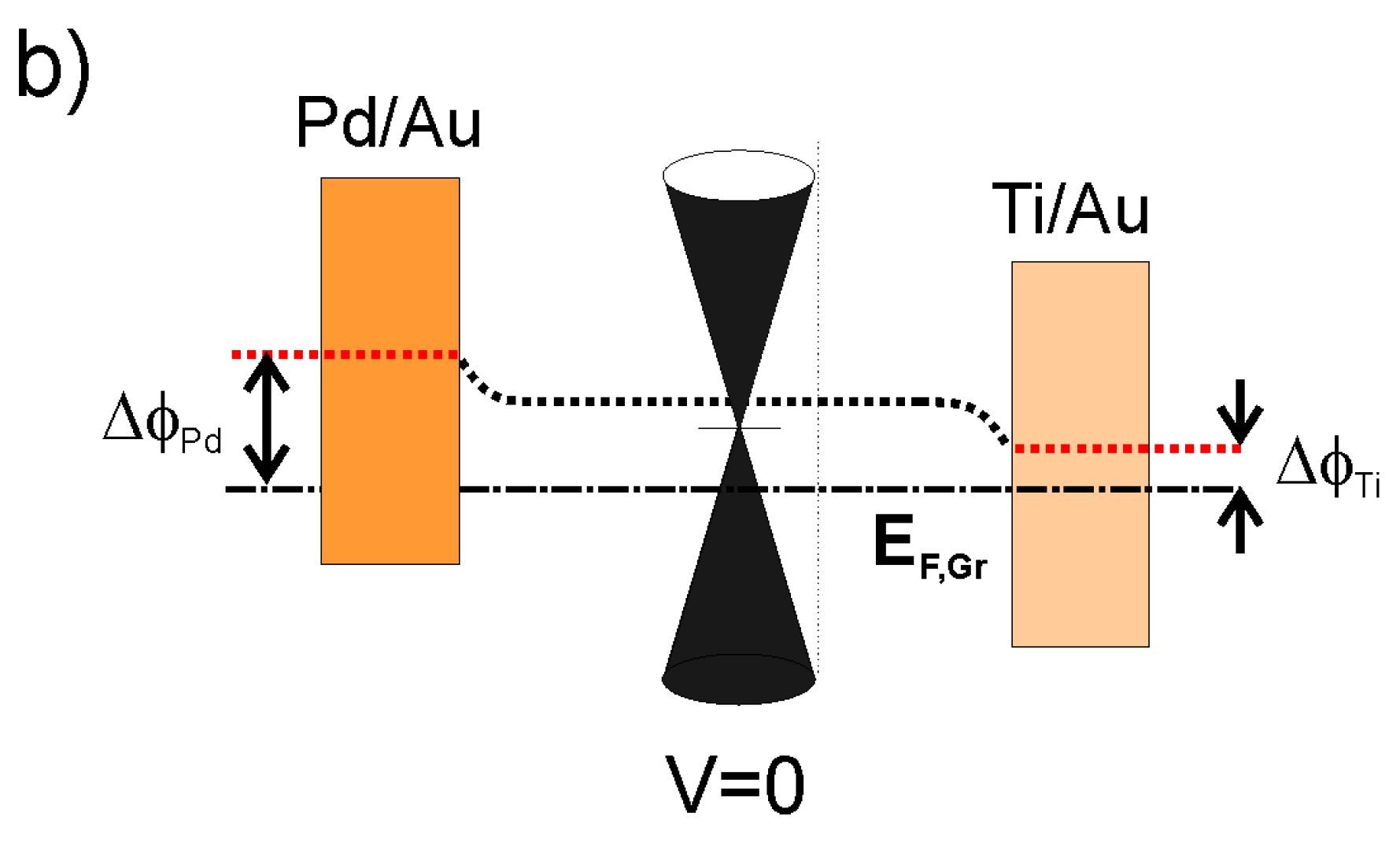
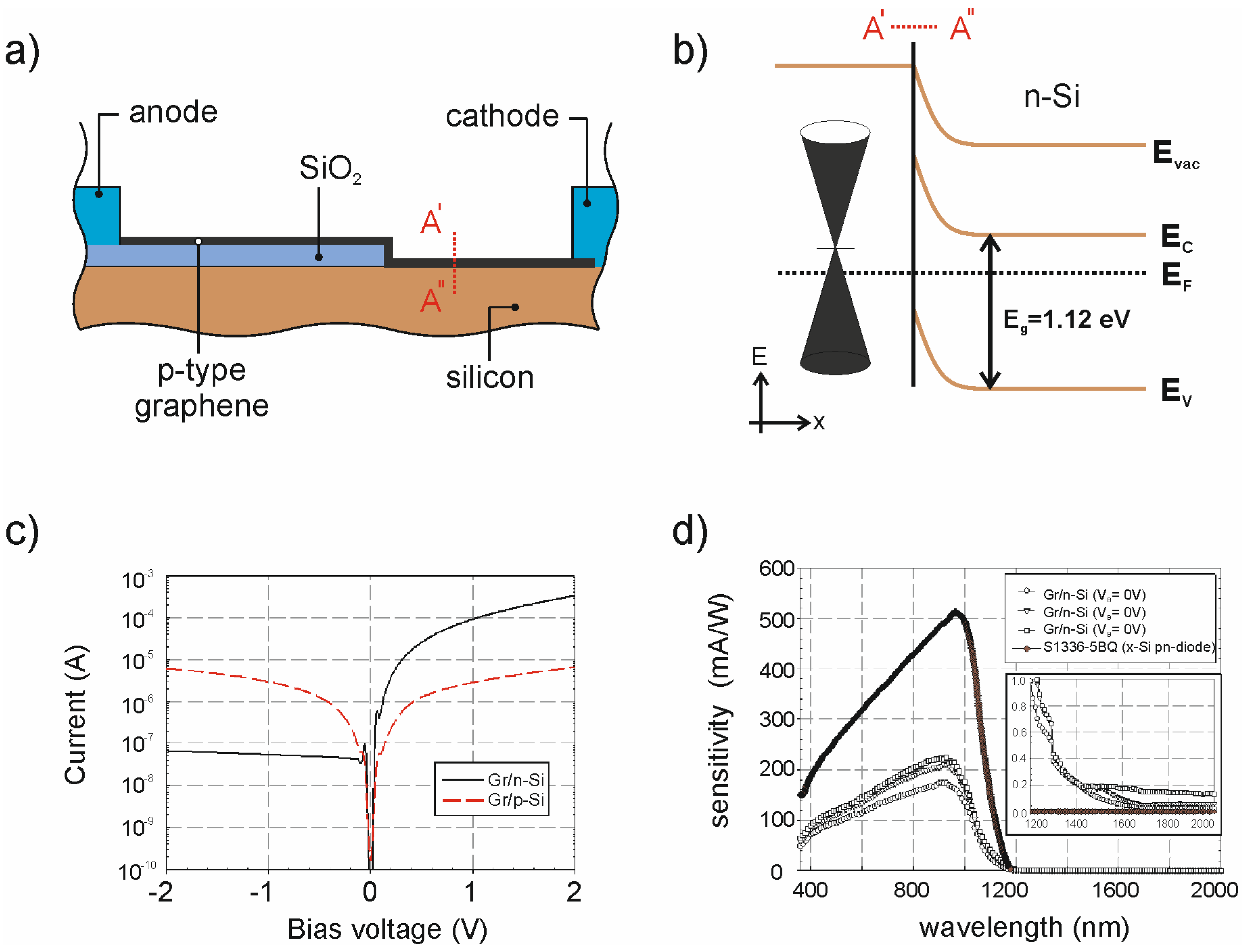
4.1. Graphene Photodetectors
4.2. TMD Photodetectors
5. Conclusions
Acknowledgments
Author Contributions
Conflicts of Interest
References
- Novoselov, K.S.; Fal’ko, V.I.; Colombo, L.; Gellert, P.R.; Schwab, M.G.; Kim, K. A roadmap for graphene. Nature 2012, 490, 192–200. [Google Scholar] [CrossRef] [PubMed]
- Nair, R.R.; Blake, P.; Grigorenko, A.N.; Novoselov, K.S.; Booth, T.J.; Stauber, T.; Peres, N.M.R.; Geim, A.K. Fine structure constant defines visual transparency of graphene. Science 2008, 320, 1308. [Google Scholar] [CrossRef] [PubMed]
- Kuzmenko, A.B.; van Heumen, E.; Carbone, F.; van der Marel, D. Universal optical conductance of graphite. Phys. Rev. Lett. 2008, 100, 117401. [Google Scholar] [CrossRef] [PubMed]
- Pang, S.; Hernandez, Y.; Feng, X.; Müllen, K. Graphene as transparent electrode material for organic electronics. Adv. Mater. 2011, 23, 2779–2795. [Google Scholar] [CrossRef] [PubMed]
- Li, Z.Q.; Henriksen, E.A.; Jiang, Z.; Hao, Z.; Martin, M.C.; Kim, P.; Stormer, H.L.; Basov, D.N. Dirac charge dynamics in graphene by infrared spectroscopy. Nat. Phys. 2008, 4, 532–535. [Google Scholar] [CrossRef]
- Bernardi, M.; Palummo, M.; Grossman, J.C. Extraordinary sunlight absorption and one nanometer thick photovoltaics using two-dimensional monolayer materials. Nano Lett. 2013, 13, 3664–3670. [Google Scholar] [CrossRef] [PubMed]
- Splendiani, A.; Sun, L.; Zhang, Y.; Li, T.; Kim, J.; Chim, C.-Y.; Galli, G.; Wang, F. Emerging photoluminescence in monolayer MoS2. Nano Lett. 2010, 10, 1271–1275. [Google Scholar] [CrossRef] [PubMed]
- Li, J.; Majety, S.; Dahal, R.; Zhao, W.P.; Lin, J.Y.; Jiang, H.X. Dielectric strength, optical absorption, and deep ultraviolet detectors of hexagonal boron nitride epilayers. Appl. Phys. Lett. 2012, 101, 171112. [Google Scholar] [CrossRef]
- Kataria, S.; Wagner, S.; Ruhkopf, J.; Gahoi, A.; Pandey, H.; Bornemann, R.; Vaziri, S.; Smith, A.D.; Ostling, M.; Lemme, M.C. Chemical vapor deposited graphene: From synthesis to applications. Phys. Status Solidi A 2014, 211, 2439–2449. [Google Scholar] [CrossRef]
- Chhowalla, M.; Shin, H.S.; Eda, G.; Li, L.-J.; Loh, K.P.; Zhang, H. The chemistry of two-dimensional layered transition metal dichalcogenide nanosheets. Nat. Chem. 2013, 5, 263–275. [Google Scholar] [CrossRef] [PubMed]
- Yamada, T.; Kim, J.; Ishihara, M.; Hasegawa, M. Low-temperature graphene synthesis using microwave plasma CVD. J. Phys. Appl. Phys. 2013, 46, 063001. [Google Scholar] [CrossRef]
- Smith, A.; Vaziri, S.; Rodriguez, S.; Östling, M.; Lemme, M.C. Wafer scale graphene transfer for back end of the line device integration. In Proceedings of the 2014 15th International Conference on Ultimate Integration on Silicon (ULIS), Stockholm, Sweden, 7–9 April 2014.
- Banszerus, L.; Schmitz, M.; Engels, S.; Dauber, J.; Oellers, M.; Haupt, F.; Watanabe, K.; Taniguchi, T.; Beschoten, B.; Stampfer, C. Ultrahigh-mobility graphene devices from chemical vapor deposition on reusable copper. Sci. Adv. 2015, 1, e1500222. [Google Scholar] [CrossRef] [PubMed]
- Lupina, G.; Kitzmann, J.; Costina, I.; Lukosius, M.; Wenger, C.; Wolff, A.; Vaziri, S.; Östling, M.; Pasternak, I.; Krajewska, A.; et al. Residual metallic contamination of transferred chemical vapor deposited graphene. ACS Nano 2015. [Google Scholar] [CrossRef] [PubMed]
- Wagner, S.; Weisenstein, C.; Smith, A.D.; Östling, M.; Kataria, S.; Lemme, M.C. Graphene transfer methods for the fabrication of membrane-based NEMS devices. Microelectron. Eng. 2016, 159, 108–113. [Google Scholar] [CrossRef]
- Bae, S.; Kim, H.; Lee, Y.; Xu, X.; Park, J.-S.; Zheng, Y.; Balakrishnan, J.; Lei, T.; Kim, H.R.; Song, Y.I.; et al. Roll-to-roll production of 30-inch graphene films for transparent electrodes. Nat. Nanotechnol. 2010, 5, 574–578. [Google Scholar] [CrossRef] [PubMed]
- Rahimi, S.; Tao, L.; Chowdhury, S.F.; Park, S.; Jouvray, A.; Buttress, S.; Rupesinghe, N.; Teo, K.; Akinwande, D. Toward 300 mm wafer-scalable high-performance polycrystalline chemical vapor deposited graphene transistors. ACS Nano 2014, 8, 10471–10479. [Google Scholar] [CrossRef] [PubMed]
- Bae, S.; Kim, S.J.; Shin, D.; Ahn, J.-H.; Hong, B.H. Towards industrial applications of graphene electrodes. Phys. Scr. 2012, 2012, 014024. [Google Scholar] [CrossRef]
- Bablich, A.; Watty, K.; Merfort, C.; Seibel, K.; Boehm, M. A novel high-dynamic A-Si:H multicolor pin-detector with ZnO:Al front and back contacts. In Proceedings of the 2010 MRS Fall Meeting: Symposium AA—Group IV Semiconductor Nanostructures and Applications, Boston, MA, USA, 29 November–3 December 2010; Volume 1305.
- Hamberg, I.; Granqvist, C.G. Evaporated Sn-doped In2O3 films: Basic optical properties and applications to energy-efficient windows. J. Appl. Phys. 1986, 60, R123–R160. [Google Scholar] [CrossRef]
- Minami, T. Transparent conducting oxide semiconductors for transparent electrodes. Semicond. Sci. Technol. 2005, 20, S35–S44. [Google Scholar] [CrossRef]
- Granqvist, C.G. Transparent conductors as solar energy materials: A panoramic review. Sol. Energy Mater. Sol. Cells 2007, 91, 1529–1598. [Google Scholar] [CrossRef]
- Engadget. Samsung Showcases 4.5-Inch Flexible AMOLED, May Actually Mass Produce This One. Available online: http://www.engadget.com/2010/11/04/samsung-showcases-4-5-inch-flexible-amoled-may-actually-mass-pr/ (accessed on 1 October 2015).
- Pocket-Lint. Plastic Logic Shows Off Colour e-Paper Display Smart Watch Concept: The Future of Wearable Tech? Available online: http://www.pocket-lint.com/news/120209-plastic-logic-colour-e-paper-smart-watch-concept (accessed on 1 October 2015).
- Koppens, F.H.L.; Mueller, T.; Avouris, P.; Ferrari, A.C.; Vitiello, M.S.; Polini, M. Photodetectors based on graphene, other two-dimensional materials and hybrid systems. Nat. Nanotechnol. 2014, 9, 780–793. [Google Scholar] [CrossRef] [PubMed]
- Wu, Z.; Chen, Z.; Du, X.; Logan, J.M.; Sippel, J.; Nikolou, M.; Kamaras, K.; Reynolds, J.R.; Tanner, D.B.; Hebard, A.F.; et al. Transparent, conductive carbon nanotube films. Science 2004, 305, 1273–1276. [Google Scholar] [CrossRef] [PubMed]
- De, S.; Coleman, J.N. Are there fundamental limitations on the sheet resistance and transmittance of thin graphene films? ACS Nano 2010, 4, 2713–2720. [Google Scholar] [CrossRef] [PubMed]
- Lee, J.-Y.; Connor, S.T.; Cui, Y.; Peumans, P. Solution-processed metal nanowire mesh transparent electrodes. Nano Lett. 2008, 8, 689–692. [Google Scholar] [CrossRef] [PubMed]
- Bonaccorso, F.; Sun, Z.; Hasan, T.; Ferrari, A.C. Graphene photonics and optoelectronics. Nat. Photonics 2010, 4, 611–622. [Google Scholar] [CrossRef]
- Sahu, D.R.; Lin, S.-Y.; Huang, J.-L. ZnO/Ag/ZnO multilayer films for the application of a very low resistance transparent electrode. Appl. Surf. Sci. 2006, 252, 7509–7514. [Google Scholar] [CrossRef]
- De, S.; Higgins, T.M.; Lyons, P.E.; Doherty, E.M.; Nirmalraj, P.N.; Blau, W.J.; Boland, J.J.; Coleman, J.N. Silver nanowire networks as flexible, transparent, conducting films: Extremely high dc to optical conductivity ratios. ACS Nano 2009, 3, 1767–1774. [Google Scholar] [CrossRef] [PubMed]
- Vivien, L.; Polzer, A.; Marris-Morini, D.; Osmond, J.; Hartmann, J.M.; Crozat, P.; Cassan, E.; Kopp, C.; Zimmermann, H.; Fédéli, J.M. Zero-bias 40 Gbit/s germanium waveguide photodetector on silicon. Opt. Express 2012, 20, 1096–1101. [Google Scholar] [CrossRef] [PubMed]
- Wirths, S.; Geiger, R.; von den Driesch, N.; Mussler, G.; Stoica, T.; Mantl, S.; Ikonic, Z.; Luysberg, M.; Chiussi, S.; Hartmann, J.M. Lasing in direct-bandgap GeSn alloy grown on Si. Nat. Photonics 2015, 9, 88–92. [Google Scholar] [CrossRef]
- Lemme, M.C.; Koppens, F.H.L.; Falk, A.L.; Rudner, M.S.; Park, H.; Levitov, L.S.; Marcus, C.M. Gate-activated photoresponse in a graphene p–n junction. Nano Lett. 2011, 11, 4134–4137. [Google Scholar] [CrossRef] [PubMed]
- Farmer, D.B.; Golizadeh-Mojarad, R.; Perebeinos, V.; Lin, Y.-M.; Tulevski, G.S.; Tsang, J.C.; Avouris, P. Chemical doping and electron-hole conduction asymmetry in graphene devices. Nano Lett. 2008, 9, 388–392. [Google Scholar] [CrossRef] [PubMed]
- Sherpa, S.D.; Kunc, J.; Hu, Y.; Levitin, G.; de Heer, W.A.; Berger, C.; Hess, D.W. Local work function measurements of plasma-fluorinated epitaxial graphene. Appl. Phys. Lett. 2014, 104, 081607. [Google Scholar] [CrossRef]
- Mueller, T.; Xia, F.; Avouris, P. Graphene photodetectors for high-speed optical communications. Nat. Photonics 2010, 4, 297–301. [Google Scholar] [CrossRef]
- Rao, G.; Freitag, M.; Chiu, H.-Y.; Sundaram, R.S.; Avouris, P. Raman and photocurrent imaging of electrical stress-induced p–n junctions in graphene. ACS Nano 2011, 5, 5848–5854. [Google Scholar] [CrossRef] [PubMed]
- Freitag, M.; Low, T.; Xia, F.; Avouris, P. Photoconductivity of biased graphene. Nat. Photonics 2013, 7, 53–59. [Google Scholar] [CrossRef]
- Gabor, N.M.; Song, J.C.W.; Ma, Q.; Nair, N.L.; Taychatanapat, T.; Watanabe, K.; Taniguchi, T.; Levitov, L.S.; Jarillo-Herrero, P. Hot carrier–assisted intrinsic photoresponse in graphene. Science 2011, 334, 648–652. [Google Scholar] [CrossRef] [PubMed]
- Song, J.C.W.; Rudner, M.S.; Marcus, C.M.; Levitov, L.S. Hot carrier transport and photocurrent response in graphene. Nano Lett. 2011, 11, 4688–4692. [Google Scholar] [CrossRef] [PubMed]
- Kim, M.-H.; Yan, J.; Suess, R.J.; Murphy, T.E.; Fuhrer, M.S.; Drew, H.D. Photothermal response in dual-gated bilayer graphene. Phys. Rev. Lett. 2013, 110, 247402. [Google Scholar] [CrossRef] [PubMed]
- Tielrooij, K.J.; Song, J.C.W.; Jensen, S.A.; Centeno, A.; Pesquera, A.; Zurutuza Elorza, A.; Bonn, M.; Levitov, L.S.; Koppens, F.H.L. Photoexcitation cascade and multiple hot-carrier generation in graphene. Nat. Phys. 2013, 9, 248–252. [Google Scholar] [CrossRef]
- Freitag, M.; Low, T.; Avouris, P. Increased responsivity of suspended graphene photodetectors. Nano Lett. 2013, 13, 1644–1648. [Google Scholar] [CrossRef] [PubMed]
- Park, J.; Ahn, Y.H.; Ruiz-Vargas, C. Imaging of photocurrent generation and collection in single-layer graphene. Nano Lett. 2009, 9, 1742–1746. [Google Scholar] [CrossRef] [PubMed]
- Lee, E.J.H.; Balasubramanian, K.; Weitz, R.T.; Burghard, M.; Kern, K. Contact and edge effects in graphene devices. Nat. Nanotechnol. 2008, 3, 486–490. [Google Scholar] [CrossRef] [PubMed]
- Xia, F.; Mueller, T.; Golizadeh-Mojarad, R.; Freitag, M.; Lin, Y.; Tsang, J.; Perebeinos, V.; Avouris, P. Photocurrent imaging and efficient photon detection in a graphene transistor. Nano Lett. 2009, 9, 1039–1044. [Google Scholar] [CrossRef] [PubMed]
- Mueller, T.; Xia, F.; Freitag, M.; Tsang, J.; Avouris, P. Role of contacts in graphene transistors: A scanning photocurrent study. Phys. Rev. B 2009, 79, 245430. [Google Scholar] [CrossRef]
- Withers, F.; Bointon, T.H.; Craciun, M.F.; Russo, S. All-graphene photodetectors. ACS Nano 2013, 7, 5052–5057. [Google Scholar] [CrossRef] [PubMed] [Green Version]
- Echtermeyer, T.J.; Nene, P.S.; Trushin, M.; Gorbachev, R.V.; Eiden, A.L.; Milana, S.; Sun, Z.; Schliemann, J.; Lidorikis, E.; Novoselov, K.S.; et al. Photothermoelectric and photoelectric contributions to light detection in metal–graphene–metal photodetectors. Nano Lett. 2014, 14, 3733–3742. [Google Scholar] [CrossRef] [PubMed]
- Pospischil, A.; Humer, M.; Furchi, M.M.; Bachmann, D.; Guider, R.; Fromherz, T.; Mueller, T. CMOS-compatible graphene photodetector covering all optical communication bands. Nat. Photonics 2013, 7, 892–896. [Google Scholar] [CrossRef]
- Naiini, M.M.; Vaziri, S.; Smith, A.D.; Lemme, M.C.; Ostling, M. Embedded graphene photodetectors for silicon photonics. In Proceedings of the 2014 72nd Annual Device Research Conference (DRC), Santa Barbara, CA, USA, 22–25 June 2014; pp. 43–44.
- Liu, M.; Yin, X.; Ulin-Avila, E.; Geng, B.; Zentgraf, T.; Ju, L.; Wang, F.; Zhang, X. A graphene-based broadband optical modulator. Nature 2011, 474, 64–67. [Google Scholar] [CrossRef] [PubMed]
- Schall, D.; Neumaier, D.; Mohsin, M.; Chmielak, B.; Bolten, J.; Porschatis, C.; Prinzen, A.; Matheisen, C.; Kuebart, W.; Junginger, B.; et al. 50 GBit/s photodetectors based on wafer-scale graphene for integrated silicon photonic communication systems. ACS Photonics 2014, 1, 781–784. [Google Scholar] [CrossRef]
- Chen, L.; Lipson, M. Ultra-low capacitance and high speed germanium photodetectors on silicon. Opt. Express 2009, 17, 7901–7906. [Google Scholar] [CrossRef] [PubMed]
- Chen, C.-C.; Aykol, M.; Chang, C.-C.; Levi, A.F.J.; Cronin, S.B. Graphene-silicon schottky diodes. Nano Lett. 2011, 11, 1863–1867. [Google Scholar] [CrossRef] [PubMed]
- Riazimehr, S.; Schneider, D.; Yim, C.; Kataria, S.; Passi, V.; Bablich, A.; Duesberg, G.S.; Lemme, M.C. Spectral sensitivity of a graphene/silicon pn-junction photodetector. In Proceedings of the 2015 Joint International EUROSOI Workshop and International Conference on Ultimate Integration on Silicon (EUROSOI-ULIS), Bologna, Italy, 26–28 January 2015.
- Smith, A.D.; Elgammal, K.; Niklaus, F.; Delin, A.; Fischer, A.C.; Vaziri, S.; Forsberg, F.; Råsander, M.; Hugosson, H.; Bergqvist, L.; et al. Resistive graphene humidity sensors with rapid and direct electrical readout. Nanoscale 2015, 7, 19099–19109. [Google Scholar] [CrossRef] [PubMed]
- Cusati, T.; Fiori, G.; Gahoi, A.; Fortunelli, A.; Lemme, M.C.; Iannaccone, G. Electrical properties of graphene-metal contacts.: A theoretical and experimental study. In Proceedings of The IEEE International Electron Device Meeting IEDM, Washington, DC, USA, 7–9 December 2015.
- An, X.; Liu, F.; Jung, Y.J.; Kar, S. Tunable graphene–silicon heterojunctions for ultrasensitive photodetection. Nano Lett. 2013, 13, 909–916. [Google Scholar] [CrossRef] [PubMed]
- Kim, H.-Y.; Lee, K.; McEvoy, N.; Yim, C.; Duesberg, G.S. Chemically modulated graphene diodes. Nano Lett. 2013, 13, 2182–2188. [Google Scholar] [CrossRef] [PubMed]
- Winzer, T.; Knorr, A.; Malic, E. Carrier multiplication in graphene. Nano Lett. 2010, 10, 4839–4843. [Google Scholar] [CrossRef] [PubMed]
- Plötzing, T.; Winzer, T.; Malic, E.; Neumaier, D.; Knorr, A.; Kurz, H. Experimental verification of carrier multiplication in graphene. Nano Lett. 2014, 14, 5371–5375. [Google Scholar] [CrossRef] [PubMed]
- Zhang, J.; Zhu, Z.; Liu, W.; Yuan, X.; Qin, S. Graphene Plasmonics for Light Trapping and Absorption Engineering in optoelectronic devices; Frontiers in Optics: San Diego, CA, USA, 2015. [Google Scholar]
- Peters, E.C.; Lee, E.J.H.; Burghard, M.; Kern, K. Gate dependent photocurrents at a graphene p–n junction. Appl. Phys. Lett. 2010, 97, 193102. [Google Scholar] [CrossRef]
- Gilbertson, A.M.; Francescato, Y.; Roschuk, T.; Shautsova, V.; Chen, Y.; Sidiropoulos, T.P.H.; Hong, M.; Giannini, V.; Maier, S.A.; Cohen, L.F.; et al. Plasmon-induced optical anisotropy in hybrid graphene–metal nanoparticle systems. Nano Lett. 2015, 15, 3458–3464. [Google Scholar] [CrossRef] [PubMed]
- Engel, M.; Steiner, M.; Lombardo, A.; Ferrari, A.C.; v Löhneysen, H.; Avouris, P.; Krupke, R. Light–matter interaction in a microcavity-controlled graphene transistor. Nat. Commun. 2012, 3, 906. [Google Scholar] [CrossRef] [PubMed]
- Furchi, M.; Urich, A.; Pospischil, A.; Lilley, G.; Unterrainer, K.; Detz, H.; Klang, P.; Andrews, A.M.; Schrenk, W.; Strasser, G.; et al. Microcavity-integrated graphene photodetector. Nano Lett. 2012, 12, 2773–2777. [Google Scholar] [CrossRef] [PubMed] [Green Version]
- Liu, Y.; Cheng, R.; Liao, L.; Zhou, H.; Bai, J.; Liu, G.; Liu, L.; Huang, Y.; Duan, X. Plasmon resonance enhanced multicolour photodetection by graphene. Nat. Commun. 2011, 2, 579. [Google Scholar] [CrossRef] [PubMed]
- Huisman, E.H.; Shulga, A.G.; Zomer, P.J.; Tombros, N.; Bartesaghi, D.; Bisri, S.Z.; Loi, M.A.; Koster, L.J.A.; van Wees, B.J. High gain hybrid graphene–organic semiconductor phototransistors. ACS Appl. Mater. Interfaces 2015, 7, 11083–11088. [Google Scholar] [CrossRef] [PubMed]
- Echtermeyer, T.J.; Britnell, L.; Jasnos, P.K.; Lombardo, A.; Gorbachev, R.V.; Grigorenko, A.N.; Geim, A.K.; Ferrari, A.C.; Novoselov, K.S. Strong plasmonic enhancement of photovoltage in graphene. Nat. Commun. 2011, 2, 458. [Google Scholar] [CrossRef] [PubMed]
- Dang, V.Q.; Trung, T.Q.; Kim, D.-I.; Duy, L.T.; Hwang, B.-U.; Lee, D.-W.; Kim, B.-Y.; Toan, L.D.; Lee, N.-E. Ultrahigh responsivity in graphene–ZnO nanorod hybrid UV photodetector. Small 2015, 11, 3054–3065. [Google Scholar] [CrossRef] [PubMed]
- Konstantatos, G.; Sargent, E.H. Solution-processed quantum dot photodetectors. IEEE Proc. 2009, 97, 1666–1683. [Google Scholar] [CrossRef]
- Konstantatos, G.; Badioli, M.; Gaudreau, L.; Osmond, J.; Bernechea, M.; de Arquer, F.P.G.; Gatti, F.; Koppens, F.H.L. Hybrid graphene-quantum dot phototransistors with ultrahigh gain. Nat. Nanotechnol. 2012, 7, 363–368. [Google Scholar] [CrossRef] [PubMed]
- Zhang, D.; Gan, L.; Cao, Y.; Wang, Q.; Qi, L.; Guo, X. Understanding charge transfer at PbS-decorated graphene surfaces toward a tunable photosensor. Adv. Mater. 2012, 24, 2715–2720. [Google Scholar] [CrossRef] [PubMed]
- Sun, Z.; Liu, Z.; Li, J.; Tai, G.; Lau, S.-P.; Yan, F. Infrared photodetectors based on CVD-grown graphene and PbS quantum dots with ultrahigh responsivity. Adv. Mater. 2012, 24, 5878–5883. [Google Scholar] [CrossRef] [PubMed]
- Turyanska, L.; Makarovsky, O.; Svatek, S.A.; Beton, P.H.; Mellor, C.J.; Patanè, A.; Eaves, L.N.; Thomas, R.; Fay, M.W.; Marsden, A.J.; et al. Ligand-induced control of photoconductive gain and doping in a hybrid graphene–quantum dot transistor. Adv. Electron. Mater. 2015. [Google Scholar] [CrossRef] [Green Version]
- Zhang, Y.; Song, X.; Wang, R.; Cao, M.; Wang, H.; Che, Y.; Ding, X.; Yao, J. Comparison of photoresponse of transistors based on graphene-quantum dot hybrids with layered and bulk heterojunctions. Nanotechnology 2015, 26, 335201. [Google Scholar] [CrossRef] [PubMed]
- Lopez-Sanchez, O.; Lembke, D.; Kayci, M.; Radenovic, A.; Kis, A. Ultrasensitive photodetectors based on monolayer MoS2. Nat. Nanotechnol. 2013, 8, 497–501. [Google Scholar] [CrossRef] [PubMed]
- Zhang, W.; Huang, J.-K.; Chen, C.-H.; Chang, Y.-H.; Cheng, Y.-J.; Li, L.-J. High-gain phototransistors based on a CVD MoS2 monolayer. Adv. Mater. 2013, 25, 3456–3461. [Google Scholar] [CrossRef] [PubMed]
- Krainak, M.A.; Sun, X.; Yang, G.; Lu, W. Comparison of linear-mode avalanche photodiode lidar receivers for use at one-micron wavelength. In Proceedings of the SPIE 7681: Advanced Photon Counting Techniques IV, Orlando, FL, USA; 2010; Volume 7681, pp. 76810Y–76810Y-13. [Google Scholar]
- Kufer, D.; Konstantatos, G. Highly sensitive, encapsulated MoS2 photodetector with gate controllable gain and speed. Nano Lett. 2015, 15, 7307–7313. [Google Scholar] [CrossRef] [PubMed]
- Pospischil, A.; Furchi, M.M.; Mueller, T. Solar-energy conversion and light emission in an atomic monolayer p-n diode. Nat. Nano. 2014, 9, 257–261. [Google Scholar] [CrossRef] [PubMed]
- Lopez-Sanchez, O.; Alarcon Llado, E.; Koman, V.; Fontcuberta i Morral, A.; Radenovic, A.; Kis, A. Light generation and harvesting in a van der Waals Heterostructure. ACS Nano 2014, 8, 3042–3048. [Google Scholar] [CrossRef] [PubMed]
- Yim, C.; O’Brien, M.; McEvoy, N.; Riazimehr, S.; Schafer-Eberwein, H.; Bablich, A.; Pawar, R.; Iannaccone, G.; Downing, C.; Fiori, G.; et al. Heterojunction hybrid devices from vapor phase grown MoS2. Sci. Rep. 2014, 4, 5458. [Google Scholar] [CrossRef] [PubMed]
- Furchi, M.M.; Pospischil, A.; Libisch, F.; Burgdörfer, J.; Mueller, T. Photovoltaic effect in an electrically tunable van der Waals Heterojunction—Nano letters. Nano Lett. 2014, 14, 4785–4791. [Google Scholar] [CrossRef] [PubMed]
- Lee, C.-H.; Lee, G.-H.; van der Zande, A.M.; Chen, W.; Li, Y.; Han, M.; Cui, X.; Arefe, G.; Nuckolls, C.; Heinz, T.F.; et al. Atomically thin p–n junctions with van der Waals heterointerfaces. Nat. Nanotechnol. 2014, 9, 676–681. [Google Scholar] [CrossRef] [PubMed]
- Cheng, R.; Li, D.; Zhou, H.; Wang, C.; Yin, A.; Jiang, S.; Liu, Y.; Chen, Y.; Huang, Y.; Duan, X. Electroluminescence and photocurrent generation from atomically sharp WSe2/MoS2 heterojunction p–n diodes. Nano Lett. 2014, 14, 5590–5597. [Google Scholar] [CrossRef] [PubMed]
- Wang, Z.; Xu, K.; Li, Y.; Zhan, X.; Safdar, M.; Wang, Q.; Wang, F.; He, J. Role of Ga vacancy on a multilayer GaTe phototransistor. ACS Nano 2014, 8, 4859–4865. [Google Scholar] [CrossRef] [PubMed]
- Britnell, L.; Ribeiro, R.M.; Eckmann, A.; Jalil, R.; Belle, B.D.; Mishchenko, A.; Kim, Y.-J.; Gorbachev, R.V.; Georgiou, T.; Morozov, S.V.; et al. Strong light-matter interactions in Heterostructures of atomically thin films. Science 2013, 340, 1311–1314. [Google Scholar] [CrossRef] [PubMed]
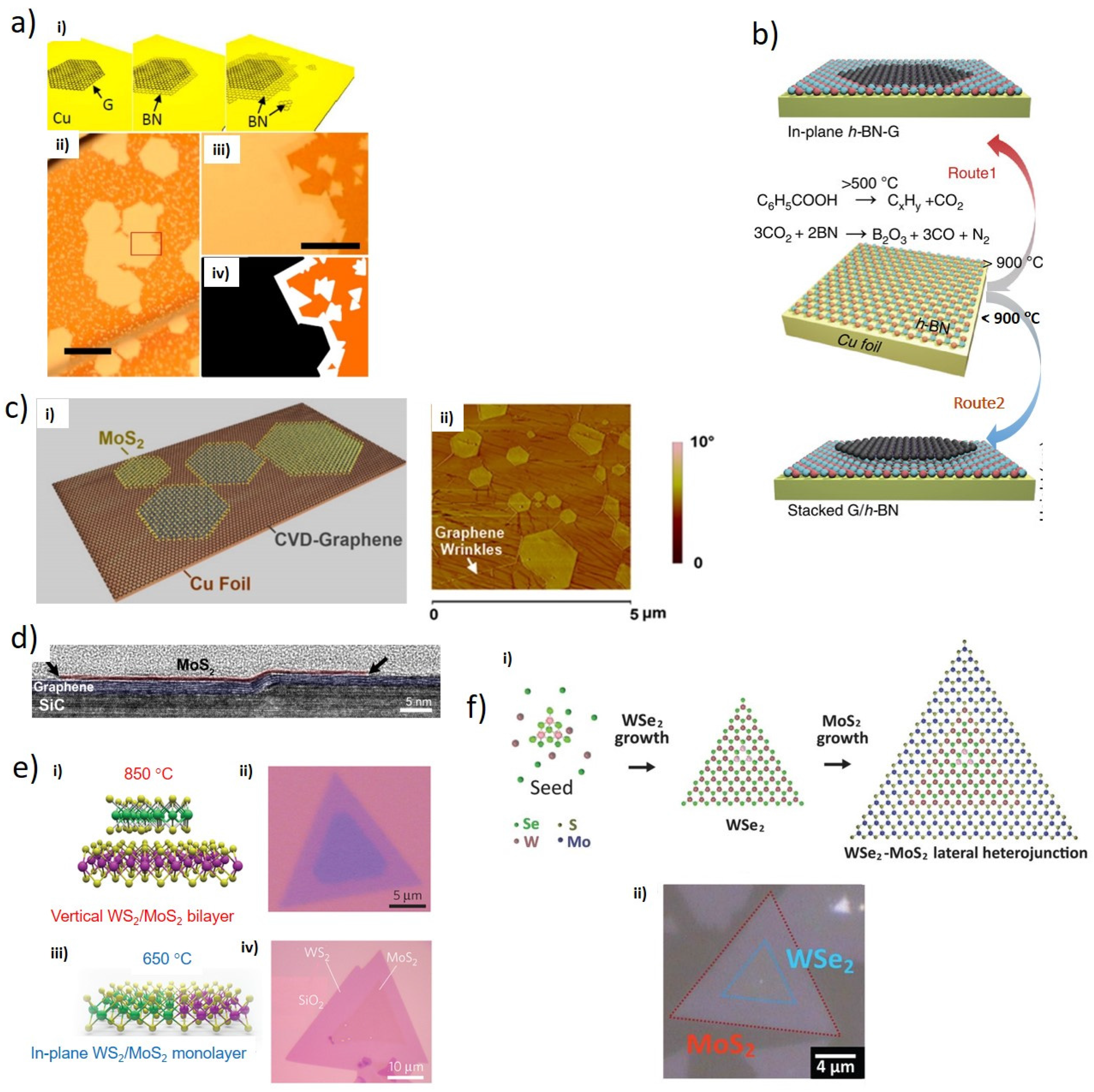
- Shi, Y.; Li, H.; Li, L.-J. Recent advances in controlled synthesis of two-dimensional transition metal dichalcogenides via vapour deposition techniques. Chem. Soc. Rev. 2015, 44, 2744–2756. [Google Scholar] [CrossRef] [PubMed]
- Han, G.H.; Rodríguez-Manzo, J.A.; Lee, C.-W.; Kybert, N.J.; Lerner, M.B.; Qi, Z.J.; Dattoli, E.N.; Rappe, A.M.; Drndic, M.; Johnson, A.T.C. Continuous growth of hexagonal graphene and boron nitride in-plane heterostructures by atmospheric pressure chemical vapor deposition. ACS Nano 2013, 7, 10129–10138. [Google Scholar] [CrossRef] [PubMed]
- Gao, T.; Song, X.; Du, H.; Nie, Y.; Chen, Y.; Ji, Q.; Sun, J.; Yang, Y.; Zhang, Y.; Liu, Z. Temperature-triggered chemical switching growth of in-plane and vertically stacked graphene-boron nitride heterostructures. Nat. Commun. 2015, 6, 6835. [Google Scholar] [CrossRef] [PubMed]
- Shi, Y.; Zhou, W.; Lu, A.-Y.; Fang, W.; Lee, Y.-H.; Hsu, A.L.; Kim, S.M.; Kim, K.K.; Yang, H.Y.; Li, L.-J.; et al. van der Waals Epitaxy of MoS2 Layers Using Graphene as Growth Templates. Nano Lett. 2012, 12, 2784–2791. [Google Scholar] [CrossRef] [PubMed]
- Lin, Y.-C.; Lu, N.; Perea-Lopez, N.; Li, J.; Lin, Z.; Peng, X.; Lee, C.H.; Sun, C.; Calderin, L.; Browning, P.N.; et al. Direct synthesis of van der Waals solids. ACS Nano 2014, 8, 3715–3723. [Google Scholar] [CrossRef]
- Gong, Y.; Lin, J.; Wang, X.; Shi, G.; Lei, S.; Lin, Z.; Zou, X.; Ye, G.; Vajtai, R.; Yakobson, B.I.; et al. Vertical and in-plane heterostructures from WS2/MoS2 monolayers. Nat. Mater. 2014, 13, 1135–1142. [Google Scholar] [CrossRef] [PubMed]
- Li, M.-Y.; Shi, Y.; Cheng, C.-C.; Lu, L.-S.; Lin, Y.-C.; Tang, H.-L.; Tsai, M.-L.; Chu, C.-W.; Wei, K.-H.; He, J.-H.; et al. Epitaxial growth of a monolayer WSe2-MoS2 lateral p–n junction with an atomically sharp interface. Science 2015, 349, 524–528. [Google Scholar] [CrossRef] [PubMed]
- Wang, X.; Cheng, Z.; Xu, K.; Tsang, H.K.; Xu, J.-B. High-responsivity graphene/silicon-heterostructure waveguide photodetectors. Nat. Photonics 2013, 7, 888–891. [Google Scholar] [CrossRef]
- Xu, K.; Xu, C.; Xie, Y.; Deng, J.; Zhu, Y.; Guo, W.; Xun, M.; Teo, K.B.K.; Chen, H.; Sun, J. Graphene GaN-based schottky ultraviolet detectors. IEEE Trans. Electron Devices 2015, 62, 2802–2808. [Google Scholar] [CrossRef]
- Spirito, D.; Coquillat, D.; Bonis, S.L.D.; Lombardo, A.; Bruna, M.; Ferrari, A.C.; Pellegrini, V.; Tredicucci, A.; Knap, W.; Vitiello, M.S. High performance bilayer-graphene terahertz detectors. Appl. Phys. Lett. 2014, 104, 061111. [Google Scholar] [CrossRef]
- Liu, Z.; Parvez, K.; Li, R.; Dong, R.; Feng, X.; Müllen, K. Transparent conductive electrodes from Graphene/PEDOT:PSS hybrid inks for ultrathin organic photodetectors. Adv. Mater. 2015, 27, 669–675. [Google Scholar] [CrossRef] [PubMed]
- Zhang, W.; Chu, C.-P.; Huang, J.-K.; Chen, C.-H.; Tsai, M.-L.; Chang, Y.-H.; Liang, C.-T.; Chen, Y.-Z.; Chueh, Y.-L.; He, J.-H.; et al. Ultrahigh-gain photodetectors based on atomically thin Graphene-MoS2 heterostructures. Sci. Rep. 2014, 4. [Google Scholar] [CrossRef] [PubMed]


| Graphene Devices | Layer No. | Technology | EQE/IQE/PCE (%) | Max. SR (mAW−1) | Ref. |
| Graphene/Si Schottky junction | SLG | CVD | --- | 270 at 992 nm 0.17 at 2000 nm | [57] |
| 3LG p-doped | IQE > 65 | 435 (850–900 nm) | [60] | ||
| SLG | --- | 320 (850–900 nm) | [60] | ||
| Graphene/Si-waveguide | SLG on Si | --- | 0.13 at 2.75 µm | [98] | |
| Graphene/GaN Schottky diode | SLG | --- | 0.23 AW−1 at 360 nm | [99] | |
| Graphene on SiO2/Si | Bilayer | Exfoliated flake | --- | 1.3 at 0.292 THz | [100] |
| Metal-graphene-metal | Bilayer | EQE = 0.5 IQE = 10 | 6.1 at 1550 nm (VIS-NIR) | [37] | |
| Graphene p–n-junction | SLG (electr. Doping) | --- | 1.5 at 532 nm (P = 30 µW) | [34] | |
| Bilayer | --- | 5 at 850 nm (T = 40 K) | [40] | ||
| Trilayer | Exfoliated, edge contacted | --- | 10 at 514.5 nm | [44] | |
| Flexible organic PDs | Graphene/PEDOT:PSS ink | Spray coating | --- | 0.16 AW−1 at 500 nm | [101] |
| TMD Devices | Layer No. | Technology | EQE/IQE/PCE (%) | Max. SR (mAW−1) | Ref. |
| MoS2 on SiO2 photoconductor | SL | Exfoliated flakes | --- | 880 A/W at 561 nm | [79] |
| WSe2 | SL (electr. doped) | PCE = 0.5 | Electroluminescent at 1.547 eV | [83] | |
| WSe2/MoS2 | SL | EQE = 2.1 | 11 at 650 nm | [86] | |
| h-BN/Gr/WS2/Gr/h-BN | SL | EQE = 30 | 0.1 at 633 nm | [90] | |
| MoS2/Si Schottky junction | 8.26 nm (12 layer) | CVD | --- | 8.6 | [85] |
| WSe2-/MoS2 pn-junction | SL p-n diode | EQE = 2.1 | 11 at 650 nm | [86] | |
| MoS2/graphene photoconductor | SLG | IQE ≈ 15 | 107 at 650 nm | [102] |
© 2016 by the authors; licensee MDPI, Basel, Switzerland. This article is an open access article distributed under the terms and conditions of the Creative Commons by Attribution (CC-BY) license (http://creativecommons.org/licenses/by/4.0/).
Share and Cite
Bablich, A.; Kataria, S.; Lemme, M.C. Graphene and Two-Dimensional Materials for Optoelectronic Applications. Electronics 2016, 5, 13. https://doi.org/10.3390/electronics5010013
Bablich A, Kataria S, Lemme MC. Graphene and Two-Dimensional Materials for Optoelectronic Applications. Electronics. 2016; 5(1):13. https://doi.org/10.3390/electronics5010013
Chicago/Turabian StyleBablich, Andreas, Satender Kataria, and Max C. Lemme. 2016. "Graphene and Two-Dimensional Materials for Optoelectronic Applications" Electronics 5, no. 1: 13. https://doi.org/10.3390/electronics5010013
APA StyleBablich, A., Kataria, S., & Lemme, M. C. (2016). Graphene and Two-Dimensional Materials for Optoelectronic Applications. Electronics, 5(1), 13. https://doi.org/10.3390/electronics5010013