Abstract
Nowadays, the analog and mixed-signal intellectual property (IP) cores play an important role in system on chip (SoC) design due to their capabilities in performing critical functions. These IPs can be the target of adversaries similar to their digital counterparts. In this work, we study the security aspects of a tunnel field effect transistor (TFET)-based six-bit successive approximation register (SAR) analog to digital converter (ADC) through proposing two threats and two countermeasures that target the output signals of the ADC datapath and its control unit. The datapath-based threat manipulates the exiting signals from the register file, and its countermeasure attempts to filter the ADC output based on the convention of having least significant bit variation (at maximum) between the adjacent sampled data points. The control-based threat manipulates the exiting signals from the control unit, and its countermeasure is a trustworthy replication of a part of the ADC circuit that is used to provide reference data for security examination and output filtering.
1. Introduction
The Internet evolution along with the recent advances in mobile technologies have changed the requirements for an electronic chip. The integrated circuit (IC) chips should provide more analog and digital functions, operate faster, and consume less power. These mixed-signal ICs are designed and fabricated using a System on Chip (SoC) technique in order to meet aggressive time to market demands. According to the SoC design technique, the analog and digital intellectual property (IP) cores are delivered by third parties and the IC designer only works on the interconnection structure between the provided modules and constructing the top module. In other words, the main circuit is built by the analog and digital sub-circuits given by external sources [1,2,3].
Employing the delivered IP cores by unknown third parties as well as the existence of diversity in the semiconductor supply chain (also known as the IC design flow) opens the possibility of applying a change to the main circuit that is known as Hardware Trojan (HT). A Hardware Trojan consists of two main elements: trigger and payload. The trigger circuit has two types: digital-based (which can be a combinational or sequential logic) and analog-based (which works based on using circuit/environmental parameters). The payload circuit is classified into three categories: digital domain (which manipulates output nodes, internal nodes, and memory content), analog domain (which manipulates analog signals such as power and timing), and system domain (which causes information leakage, denial of service, performance degradation, and heating). A Trojan should be activated by a rare event (to be sneaky) and it can be designed and inserted during design or fabrication processes by untrusted people (third party IP provider, SoC integrator, or foundry employees), design tools, or modules. Hardware Trojans can create catastrophic and life-threatening situations in critical applications such as medical devices (disrupting the communication between an implantable device and heart/brain) and military systems (misguiding the defense/offensive mechanisms). In our case, a Trojan can victimize analog and/or digital IP cores. In addition, there is no need to add more logical cells to an IC chip to create a Trojan since its circuit can be constructed using the existing cells from different regions of the chip and operate in certain condition(s) [4,5,6,7,8,9,10,11,12,13,14,15,16,17,18].
Due to the importance and critical role of signal converters in mixed-signal ICs, they can be a target for manipulation and sabotage by adversaries. An adversary may launch different attacks on these electronic modules such as HT insertion, piracy of digital and analog/mixed-signal intellectual properties, overbuilding of integrated circuits, reverse engineering, side-channels analysis, and counterfeiting. In this work, we consider infection of the employed IP cores within signal converters through inserting Hardware Trojans. Owing to these issues, the security and protection of signal converters should be taken into account in their design, fabrication, installation, and operation process. In this regard, the knowledge gained from very large scale integration (VLSI) testing can be leveraged to provide security and protection for the mixed-signal ICs. The countermeasures for Hardware Trojan attack are divided into three groups: (a) Trojan detection (such as side channel analysis, reference comparison, increasing controllability and observability, and reverse engineering); (b) design for security (such as preventing insertion and facilitating detection); and (c) monitoring and testing the system functionality externally and/or internally, which is known as built-in-self-test (BIST) [19,20].
According to the BIST, a part of an IC chip (or new added logical cells) is used to test and verify the chip partly or entirely. Depending on the chip operational condition, the BIST is classified to online and offline. In the online BIST, integrity testing and security verification occur during the active/idle mode of the normal circuit operational state. In the offline BIST, there is a certain operational state for testing and verifying the chip. There are differences when these approaches are utilized to test and verify security of digital circuits or analog/mixed-signal circuits. For example, the input data for testing digital circuits has logical (binary) nature while it is a continuous analog signal for analog/mixed-signal circuits. Many research works were done for security checking and protection provision in the digital domain [4,5,21,22,23], while only a few studies are seen in the analog/mixed-signal domain [1,2,3,24,25,26]. Due to this lack of knowledge, more research needs to be done in the area of analog/mixed-signal hardware security in order to find and develop related threats and countermeasures. In this regard, our work targets the security evaluation of a mixed-signal circuit, specifically successive approximation register (SAR) analog to digital converter (ADC).
The contributions of this paper can be stated as: (1) studying a low power six-bit SAR ADC from the security perspective; (2) proposing a threat and a countermeasure for the ADC datapath; (3) proposing a threat and a countermeasure for the ADC control unit; (4) illustrating the ADC operation flows under the proposed threats and countermeasures; and (5) analysis of the ADC functionality and performance under the the proposed threats and countermeasures. Section 2 explains the contributions in detail. The results, analysis, and discussion are presented in Section 3. The paper is concluded in Section 4.
2. Threats and Countermeasures for an SAR ADC
Most of the emitting signals from different physical objects in this world have analog nature, such as voltage, current, pressure, and temperature. In order to employ these signals in diverse computing applications, they should be transformed into the digital domain for facilitation of their processing, transmission, and storage. The process of converting an analog signal to binary data (which is a number of codes or a series of ones and zeros) is called quantization, and the electronic device that executes this function is called analog to digital conversion. The number of ADC output bits (or the ADC resolution) determines the number of quantization levels that can partition a voltage range. The reconstructed analog signal from the ADC output bits should be functionally and behaviorally close enough to the analog input signal. Functional closeness means mapping from the analog input signal to the digital output without introduction of significant quantization errors. In addition, the quantization levels should be precisely equally spaced. The behavior of the reconstructed analog signal is close to the original input signal when there is no or a small presence of performance errors and uncertainties (such as nonlinearity errors) in the converter operation. Otherwise, processing either the digital data or the reconstructed analog signal causes system abnormality. Evaluating the functional and behavioral closeness is done by checking the outputs bits and calculating the quantization error as well as performance parameters (for example, the effective number of bits).
An ADC can be infected by insertion of an HT inside the chip, with the payload of causing an intentional error during the ADC operation. The possible errors in an ADC operation are: (a) quantization, which is limitation on the signal-to-noise ratio caused by the converter finite resolution that leads to wrong output codes; (b) offset, which is the deviation between the first actual transition and the first ideal transition; (c) gain, which is the deviation between the last actual transition and the last ideal transition; (d) differential nonlinearity, which is the maximum deviation between the actual steps and the ideal steps; (e) integral nonlinearity, which is the maximum deviation between any actual transition and the endpoint correlation line; and (f) missing code, upon which the ADC does not produce one of its quantization levels for any applied analog input signal [27,28]. The missing code error is a fit candidate for a Hardware Trojan payload due to its detrimental effects in sensitive and critical applications such as medical devices and military systems, which is why we choose it in this work. Meanwhile, bit monitoring is a common testing method for missing code error to make sure that the output bits have the expected transition and there is no stuck-at-fault.
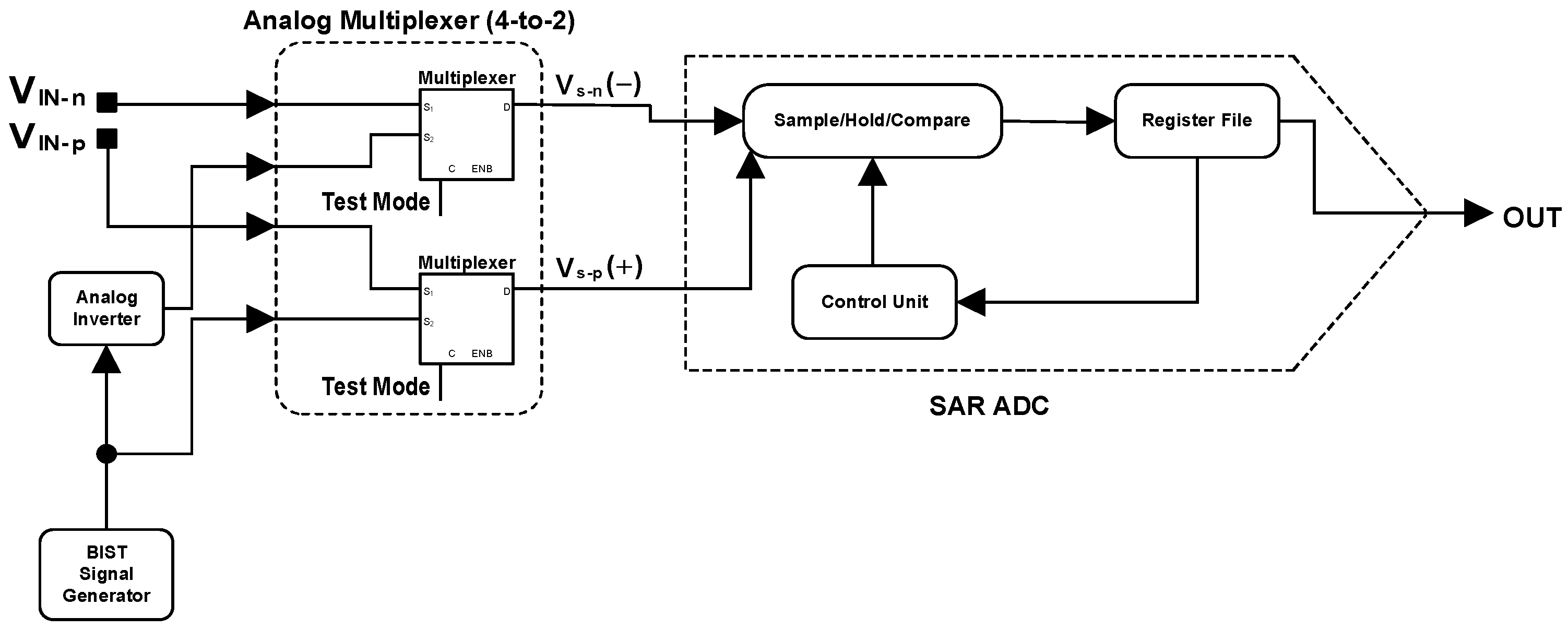
Now, we study the security of an ultra-low power six-bit successive approximation register analog-to-digital converter [29], implemented using tunnel field effect transistor technology. This ADC is power-efficient and suitable for the Internet of things (IoT) applications due to its low power consumption, small design overheads, and implementation transistor technology. The top-level architecture of this ADC along with its BIST-based input mechanism is shown in Figure 1. This architecture consists of seven main components: (1) external fully-differential analog input signal; (2) BIST signal generator; (3) analog inverter; (4) analog multiplexer; (5) sample/hold/compare (SHC); (6) register file; and (7) control unit. External fully-differential analog input signal ( and ) is the coming signal from the outside world. It can be acquired using a sensor through measuring a physical quantity of an object in differential mode. and are the negative and the positive single-ended analog input signals, respectively. BIST signal generator is responsible for producing a standard test signal with a certain waveform (such as ramp, sinusoidal, sawtooth, and triangular), frequency (or period), and amplitude internally. The produced test signal is single-ended, and its combination with the analog inverter output creates a fully-differential test signal to be sent to the analog multiplexer. Analog inverter is an analog IP for inverting the sign of the single-ended test signal in order to provide a fully-differential analog test signal to the next component.
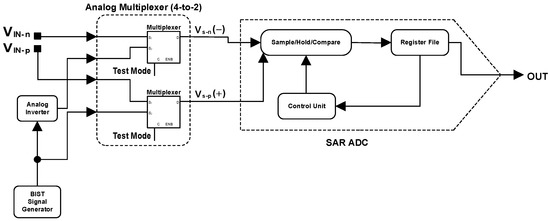
Figure 1.
The top-level architecture of an ultra-low power six-bit successive approximation register analog-to-digital converter with a built-in-self-test (BIST)-based input mechanism.
Analog multiplexer makes a decision on sending either the external fully-differential analog input signal or the fully-differential analog test signal to the SHC block, depending on the status of the “Test Mode”signal. For example, if the Test Mode signal is equal to logic one, then the fully-differential analog test signal is sent to the SHC component. This is beneficial for situations in which the external input signal is not standard and test-friendly, while the ADC needs to be tested and security checked. In addition, the status of the Test Mode signal can be determined either externally by user or internally through predefined conditions. The testing and security checking process can occur during the IC run-time operation when either the ADC is idle or it is active and the external analog input signal has a suitable waveform (such as sine) for testing. and are the exiting signals from the analog multiplexer, which are the negative and the positive single-ended analog signals under process, respectively.
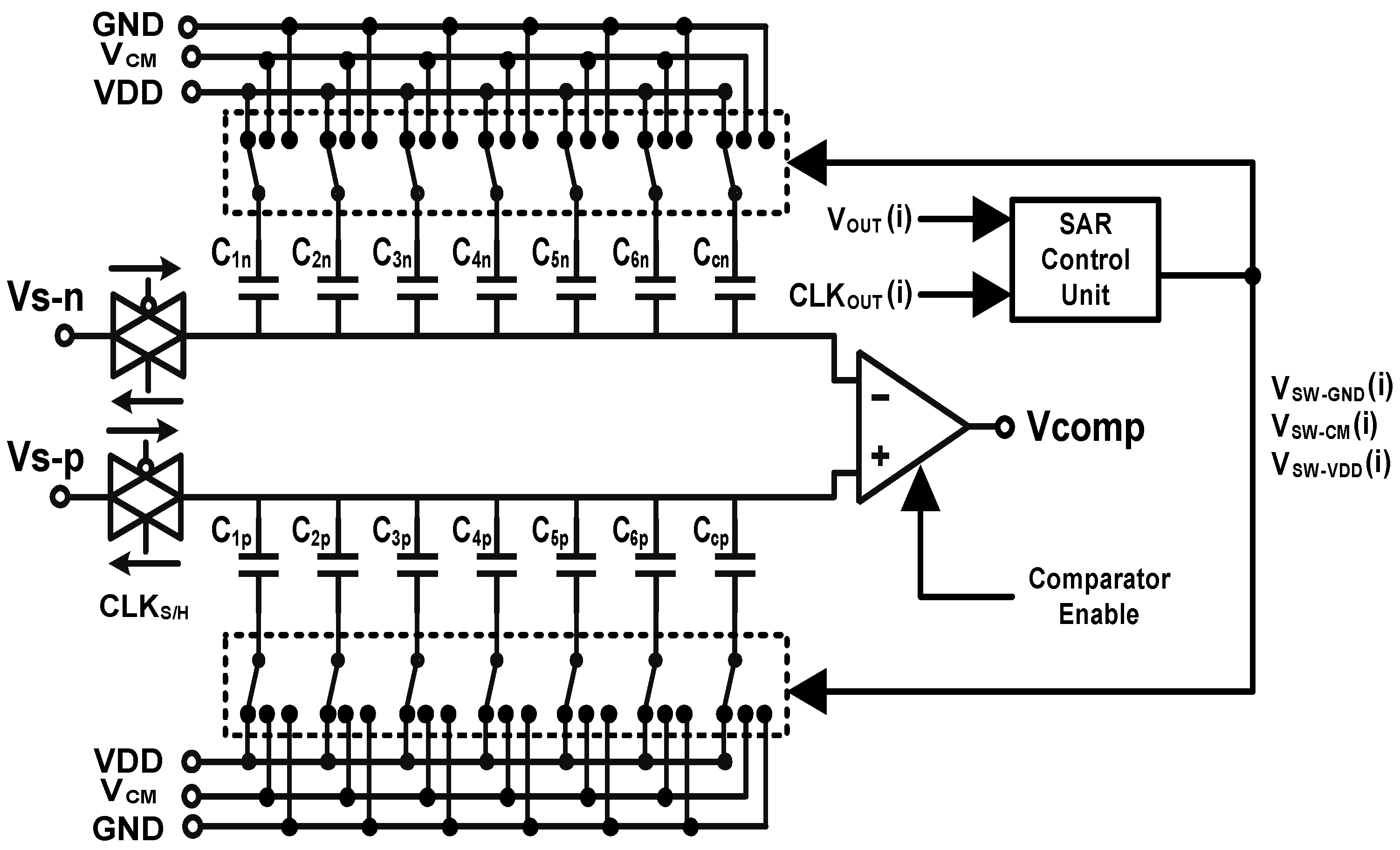
Sample/hold/compare is an analog component for sampling, holding, and comparing the entering fully-differential signal into it. The circuit for this block is shown in Figure 2. According to the circuit, there is a dedicated clock signal () for the sampling-related switches. At the beginning of each sampling, the state of approximation-related switches is restarted according to which the upper and the lower capacitor arrays are connected to entirely. The state of these switches is updated/controlled by the coming signals from the SAR control unit. The input signals to the control unit are (which is the clock signal for the flip-flop of the ith ADC output bit) and (which is the voltage signal of the ith ADC output bit). , and are the control signals for connection of the approximation-related switches to the supply voltage, common-mode voltage, and ground, respectively. is the entering data signal to the register file for construction of the ADC output bits. , and are the supply voltage, common-mode voltage, and ground, respectively. is set equal to . The comparator is actuated by the “Comparator Enable” signal.
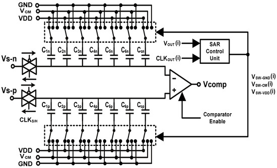
Figure 2.
The sample/hold/compare block circuit.
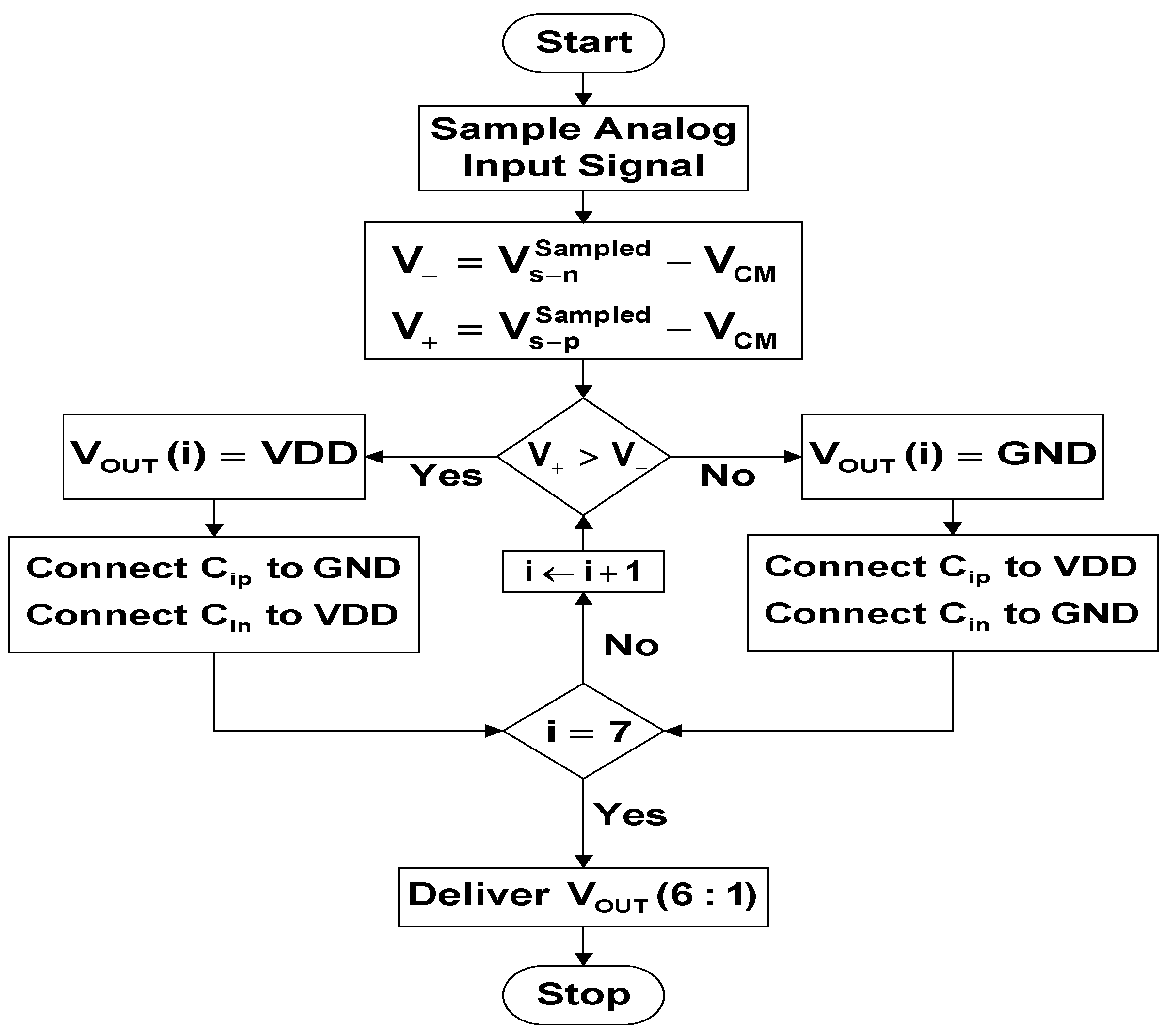
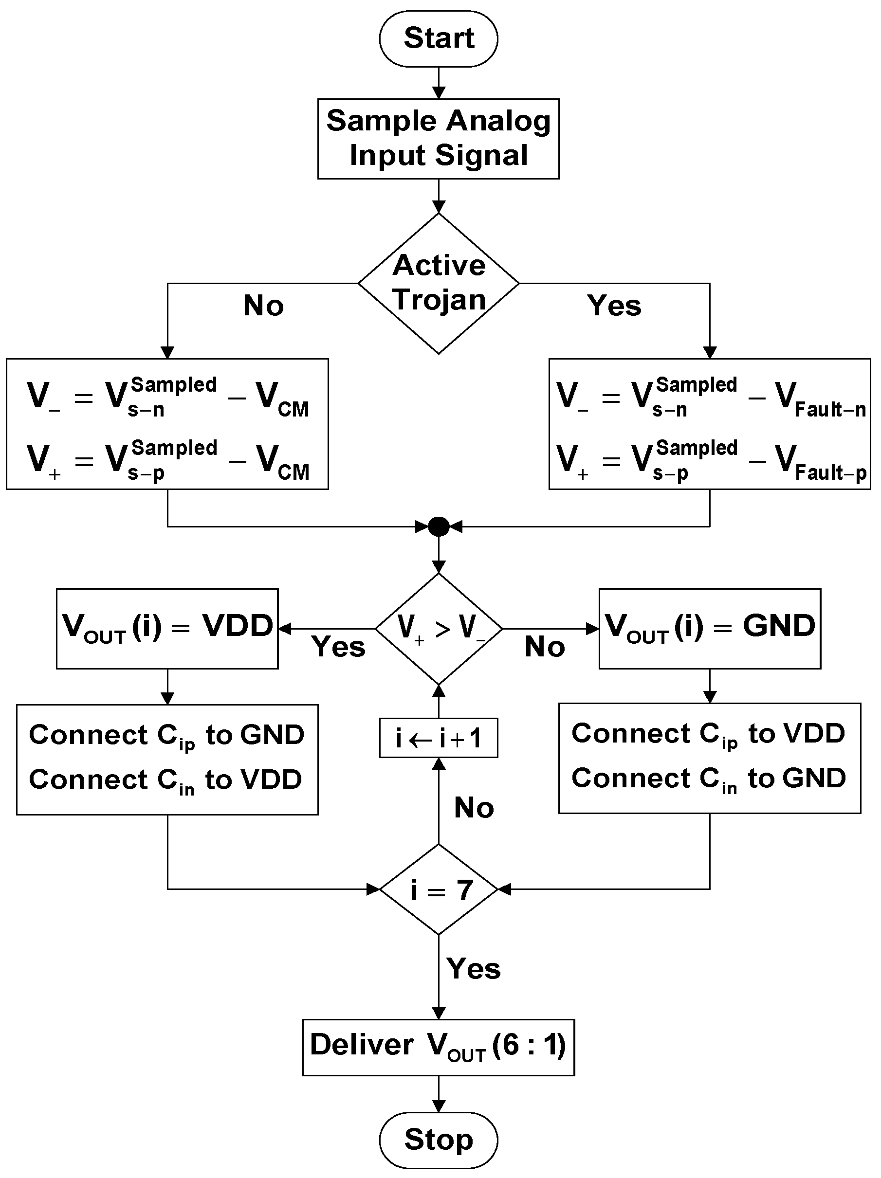
Register file is a digital IP for storing a six-bit code in D flip-flops. Each flip-flop is triggered by a proprietary clock signal. Control unit is a digital IP for generating the control signals for the approximation-related switches in the SHC block. The circuit for this block is shown in Figure 3. In this circuit, is the clock signal for the flip-flop of the ith ADC output bit, is the voltage signal of the ith ADC output bit, and , and are the control signals for connection of the approximation-related switches to the supply voltage, common-mode voltage, and ground, respectively. The delay blocks are used to provide sufficient time for readiness of the sampled signal before applying the control signal to the switches. All of the required clock signals for different parts of the ADC circuit are generated by a clock generator block that is triggered by the system clock signal (). The operation flow of the original ADC circuit is presented in Figure 4. and are the positive and negative terminals of the comparator, respectively. and are the positive and negative sampled versions of the analog input signal, respectively. According to the flowchart, a fully-differential analog input signal is sampled. The difference between the sampled signals and the common-mode voltage are applied to the comparator. If the comparator output is equal to supply voltage, then logic one is stored in the relevant flip-flop (inside the register file) and the relevant capacitors in the upper and the lower capacitor arrays are connected to ground and supply voltage, respectively, and vice versa. The process is completed by calculation of all the ADC output bits. The seventh bit is used for error checking.
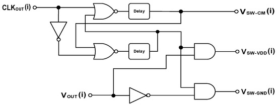
Figure 3.
The control unit block circuit.
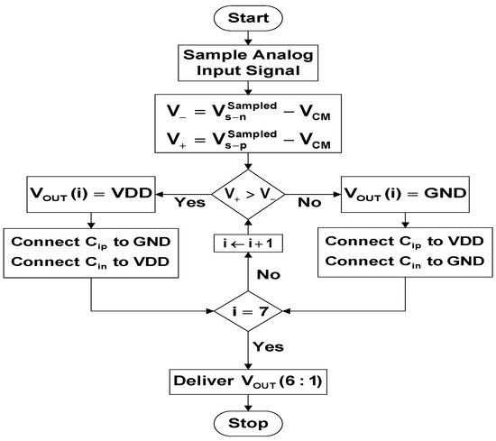
Figure 4.
The operation flow of the original analog to digital converter (ADC) circuit.
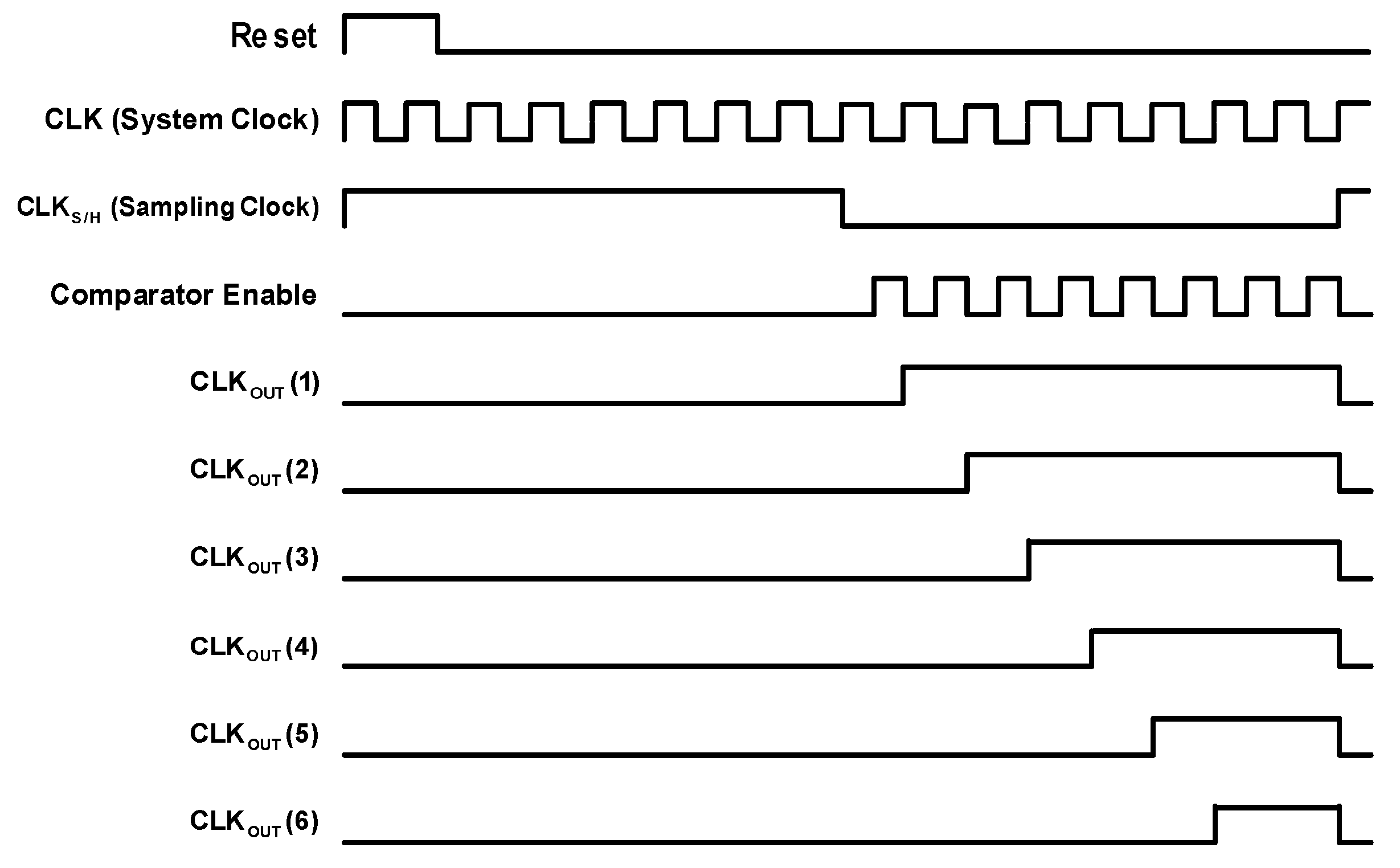
In order to satisfy the timing requirements of different components of an ADC circuit, multiple clock/trigger signals are needed that are provided by a clock generator. Figure 5 displays the timing diagram of the discussed ADC circuit according to which: (1) “Reset” signal brings the memory elements to their initial states; (2) “” is the system clock signal; (3) “” is the sampling clock signal and triggers the switches; (4) “Comparator Enable” signal is for actuating the comparator; and (5) “” is the clock signal for the flip-flop of the ith ADC output bit.
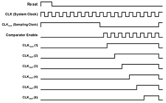
Figure 5.
The timing diagram of the ADC operation.
A central processing unit (CPU) can be attacked by subverting the functionality of its data-path and/or control unit through HT insertion [30,31]. This strategy can be utilized to attack an ADC as well. Thus, an adversary attacks both the data-path and the control unit of the ADC by infecting (or inserting a Hardware Trojan inside) the register file digital IP and the sample/hold/compare analog IP, respectively. The purpose of attack is causing the ADC malfunction “sometimes”. It is emphasized here that our designed function-targeting Hardware Trojans are not detected during the testing and verification phase since the “Mate Trigger” for the “Main Trigger” of each Hardware Trojan is generated by other parts of the SoC during the “chip run-time operation”. In other words, the mate trigger and the main trigger for each Trojan go to an AND function before being applied to the Trojan payload circuit. In this scenario, a function-targeting Hardware Trojan is never detected during the testing phase since there is no knowledge about the application that is going to be run on the chip. There is less controllability and observability on the Trojan circuit as well. With these features, the Trojans behave more sneakily. A countermeasure is proposed for each case. With respect to implementing each of the proposed Hardware Trojans, its number of logical cells may be reasonable compared to the total number of logical cells used in a system on chip. In addition, a malicious person inside the design team or the foundry might be able to employ the idle logical cells from other regions of the SoC to construct the Trojan circuit. The same concept can be applied for defense circuit implementation.
2.1. Datapath-Based Threat and Countermeasure
The plotted datapath-based threat is described as manipulation of the exiting digital signals from the register file. There are six D flip-flops inside the register file and the output of any of them can be maliciously changed sometimes. The Trojan trigger circuit is designed based on making its activation behavior “randomly” and “more sneaky”. Therefore, among the output signals of the six D flip-flops, two pair signals are selected randomly as inputs to the Trojan circuit, shown in Figure 6. According to the circuit, the two-bit shuffling unit changes the flow path of its input signals depending on the value of signal. This signal is generated by a frequency divider that is controlled by the sampling clock signal () and the last value of the Trojan enable signal (). The Trojan enabled signal is the governing signal for a multiplexer that outputs the inversion of the stored data in one of the output six flip-flops instead of the actual data. In this work, the third bit is chosen for sabotage that makes a medium-level error. A descriptive example for the circuit operation can be stated in this way: if is 0111, the top and the bottom XNOR gates output logic zero and one, respectively. Having equal to logic one in this example makes the AND gate output as well as equal to logic one, and consequently inverts the third bit of the ADC output. Figure 7 presents the operation flow of the infected ADC circuit by the datapath-based Hardware Trojan. The difference between this flowchart and the original one (shown in Figure 4) is inversion of the bit of the ADC output whenever the Trojan is activated.
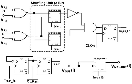
Figure 6.
The Trojan circuit for the datapath-based threat.
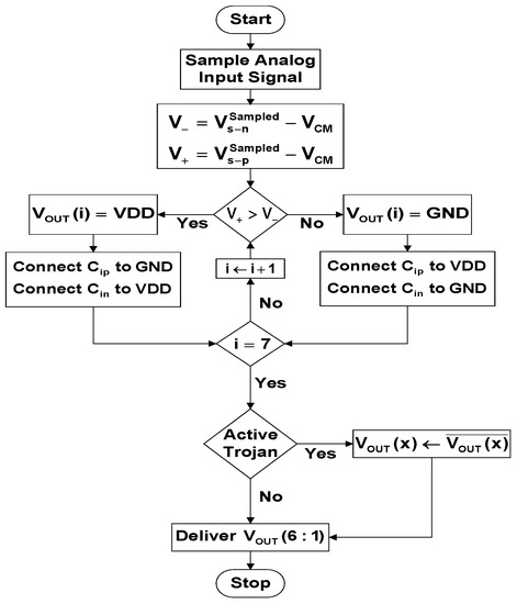
Figure 7.
The operation flow of the infected ADC circuit by the datapath-based Hardware Trojan.
The datapath-based countermeasure is designed based on this convention that the standard waveforms (for example, ramp, sine, sawtooth, and triangular) usually have least significant bit (LSB) difference between their adjacent sampled data points. In other words, the digital code for the sample point is assumed to be LSB higher, the same, or LSB lower than the ith sample point. If the ADC operation does not accommodate this convention for a sampled data point, the defense circuit (which is the inserted or internally developed BIST block) considers it as an abnormal output. Thus, the “abnormal signal” is flagged, the user is notified, and the last correct code is outputted for that data point instead of the current produced code. The defense circuit is shown in Figure 8. The is the abnormal signal, (5:0) refers to the ADC output bits before processing, (5:0) refers to the ADC output bits after processing, and the registers are used for keeping the possible cases for the next sampling point. The defense circuit causes delay in delivering the ADC output bits due to the positioned registers and the added circuit, although these registers provide synchronization and reduce the output noise significantly. In addition, the defense circuit has the capability of filtering and smoothing the sampled signal, if the analog input signal has unwanted (not necessarily malicious) large variations. A descriptive example for the circuit operation can be stated in this way: and are equal to logic zero and logic one in normal circuit operation, respectively. Consequently, is equal to logic zero and the original ADC output bits () are delivered directly. If the newly produced ADC output bits do not follow the convention (to be the same as or one bit higher/lower than the last captured ADC output bits), then and become equal to logic one due to abnormality, and the last captured data is delivered. Figure 9 presents the operation flow of the secured ADC circuit by the datapath-based defense circuit. The difference between this flowchart and the original one (shown in Figure 4) is checking the conformity of the ADC output with the described convention (and reacting in case of incompatibility) before delivering the output.
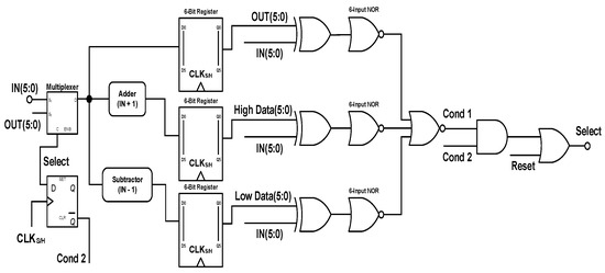
Figure 8.
The defense circuit for the datapath-based countermeasure.
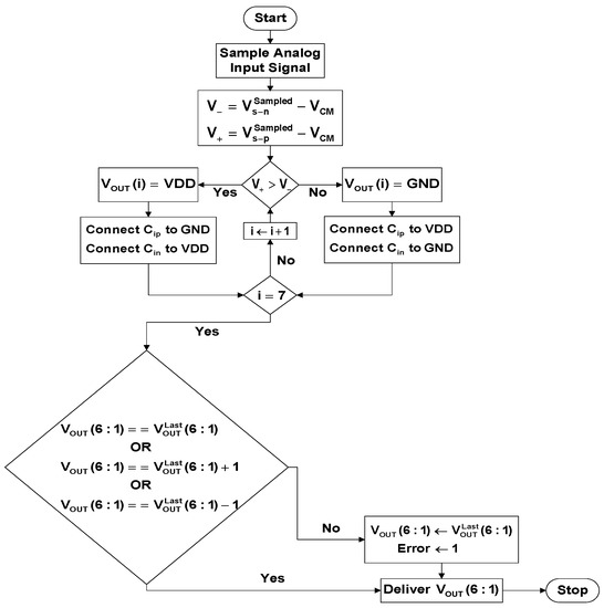
Figure 9.
The operation flow of the secured ADC circuit by the datapath-based defense circuit.
2.2. Control-Based Threat and Countermeasure
The plotted control-based threat is described as manipulation of the control signals for the approximation-related switches inside the SHC block. Normally, all of the capacitors (- and -) should be connected to at the beginning of each sampling. Next, they are connected to either or depending on the updated control signals. The designed HT has the intention of disabling the connection of one (or more) capacitor(s) to sometimes. Thus, the victim capacitor holds its charge from the last sampling and consequently one (or more number) of the ADC output bit(s) may be different than what it (they) should be. The Trojan circuit for this threat is shown in Figure 10. Its starting component is a four-bit counter that is triggered by the output signal of the analog comparator. The four output bits of the counter can construct up to sixteen Boolean functions based on the corresponding truth table. Four functions are chosen randomly (which are the 4th, 7th, 12th and 14th rows of the truth table) and built in the four-bit Minterm construction unit. Next, the functions are sent to a four-bit shuffling unit. The two-bit choice signal ( (2:1)) may be extracted from any part of the circuit to make it less dubious (or it can be made inside the SHC block). We run exclusive-OR (XOR) function on the “even” and “odd” bits of the ADC output bits to make this signal. The result bits are stored in a four-bit register that is triggered by the sampling clock. At last, the control signal for an approximation-related switch has its actual value or is zero depending on the stored data in its corresponding flip-flop in the four-bit register. We select the 2nd to 5th bits of the ADC output for malicious change. In simple words, determines either to be applied to the ith approximation-related switch or the ground. If the Trojan trigger circuit makes the value of equal to logic one, then the relevant switch is not connected to the common mode voltage at the time of sampling and incorrect results may be generated by the analog comparator. Figure 11 presents the operation flow of the infected ADC circuit by the control-based Hardware Trojan. and are the faulty voltages made by the electrical charges (remaining from the last sampling) on the victim capacitors in the upper and the lower capacitor arrays, respectively. The difference between this flowchart and the original one (shown in Figure 4) is applying “the reduction of the faulty voltages from the sampled signals” to the analog comparator when the Trojan is activated.
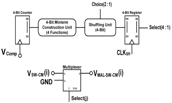
Figure 10.
The Trojan circuit for the control-based threat.
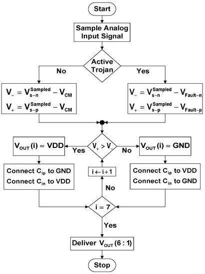
Figure 11.
The operation flow of the infected ADC circuit by the control-based Hardware Trojan.
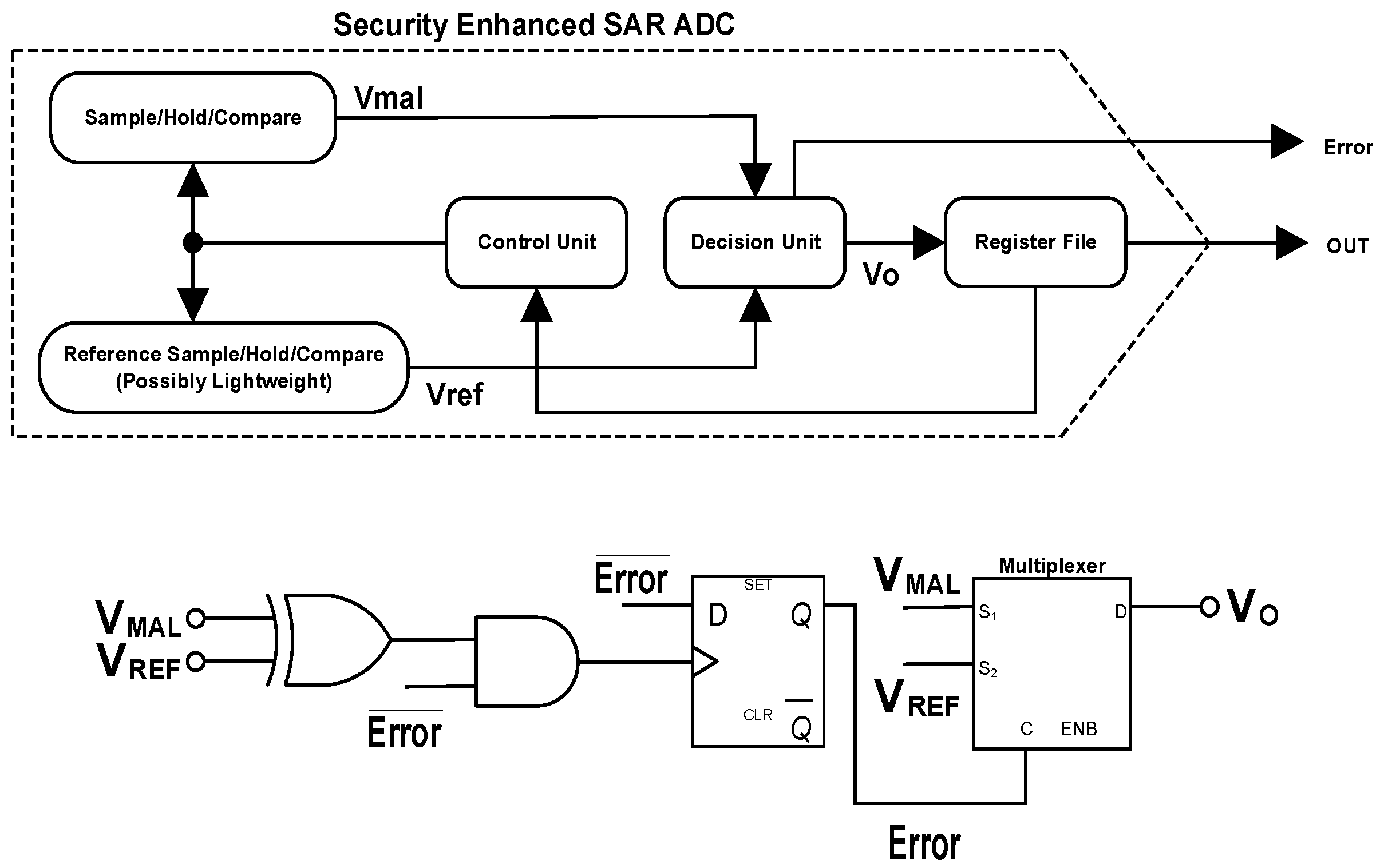
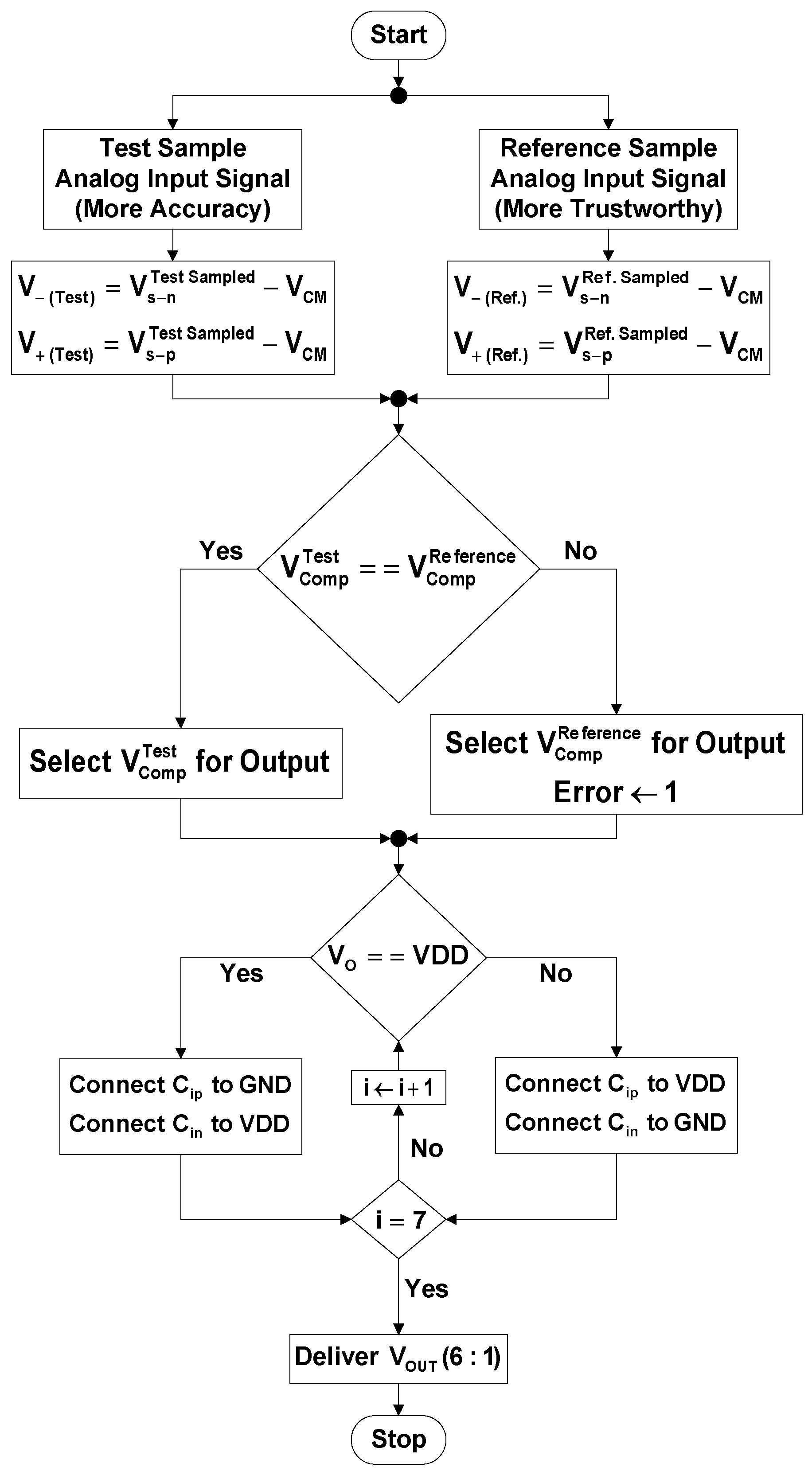
Sub-circuit replication is a common method in designing analog and digital BIST blocks [32]. The designed BIST block can be inserted or internally developed in some or all of the requested number of chips for manufacturing. The control-based countermeasure is designed based on a sub-circuit replication method, upon which a trustworthy and possibly lightweight SHC (in terms of logic simplicity and smaller capacitors) analog IP is positioned inside the chip. The outputs of the malicious SHC (or the SHC under test) and the reference lightweight SHC are sent to the decision unit for comparison and making a decision. If an error occurs, the user is notified and the reference SHC output is delivered to the register file. A lightweight reference SHC may bring lower performance and quality because of having less complexity, but it definitely provides correct functionality. The defense circuit is shown in Figure 12. and are the output voltages from the malicious and the reference SHCs and the inputs to the decision unit, which its circuit is shown in the bottom of figure. The output of the decision unit is . If equals logic one (due to the difference between the applied input voltages), then the is delivered to the next circuit stage and the user is notified. In fact, the decision unit can detect any mismatch in the “timing status” and the “logical status” of the SHCs. Figure 13 presents the operation flow of the secured ADC circuit by the control-based defense circuit. and are the outputs of the test and the reference comparators, respectively. The difference between this flowchart and the original one (shown in Figure 4) is sampling, holding, and comparing the applied analog input signal in two similar paths in order to catch any mismatch and abnormality.
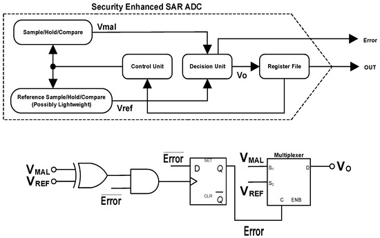
Figure 12.
The defense circuit for the control-based countermeasure.
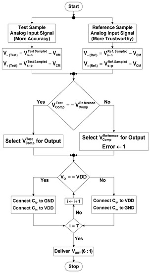
Figure 13.
The operation flow of the secured ADC circuit by the control-based defense circuit.
3. Results and Discussion
The functionality and performance of the six-bit SAR ADC for IoT low power applications [29] are evaluated in five different operating conditions: (1) “Healthy ADC”, in which no change is carried out on the ADC circuit; (2) “ADC + Attack 1”, in which the ADC is infected by the datapath-based threat; (3) “ADC + Attack 1 + Defense 1”, in which the infected ADC is defended by the datapath-based countermeasure; (4) “ADC + Attack 2”, in which the ADC is infected by the control-based threat; and (5) “ADC + Attack 2 + Defense 2”, in which the infected ADC is defended by the control-based countermeasure. We use 20 nm AlGaSb/InAs tunnel field effect transistor (TFET) technology (provided in the Universal TFET model 1.6.8 [33]) for implementation.
TFET provides steeper sub-threshold slope, smaller than 60 mV/dec [34], and is described as a gated p-i-n (which is the hole-dominant region, the intrinsic (pure) region, and the electron-dominant region) diode that has asymmetrical doping structure and operates under reverse-bias condition. The steeper sub-threshold slope of the TFET device helps further downscale the supply voltage and reduce the leakage currents substantially, which makes it an excellent candidate to achieve low energy consumption for the IoT applications. The comparison between the drain-source current () versus gate-source voltage () curves of the n-type metal–oxide–semiconductor field-effect transistor (MOSFET) and the n-type TFET is shown in Figure 14. For simulating this plot, both devices have the same width and length of 20 nm and are connected to the supply voltage of 0.6 V. As it can be seen from the figure, the TFET device turns ON and goes to its saturation region at a smaller value of the gate-source voltage compared to the MOSFET device. Thus, the TFET technology is favorable for low voltage design.
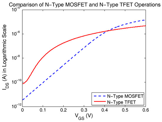
Figure 14.
The comparison between the drain-source current versus gate-source voltage curves of the N-type MOSFET and the N-type TFET.
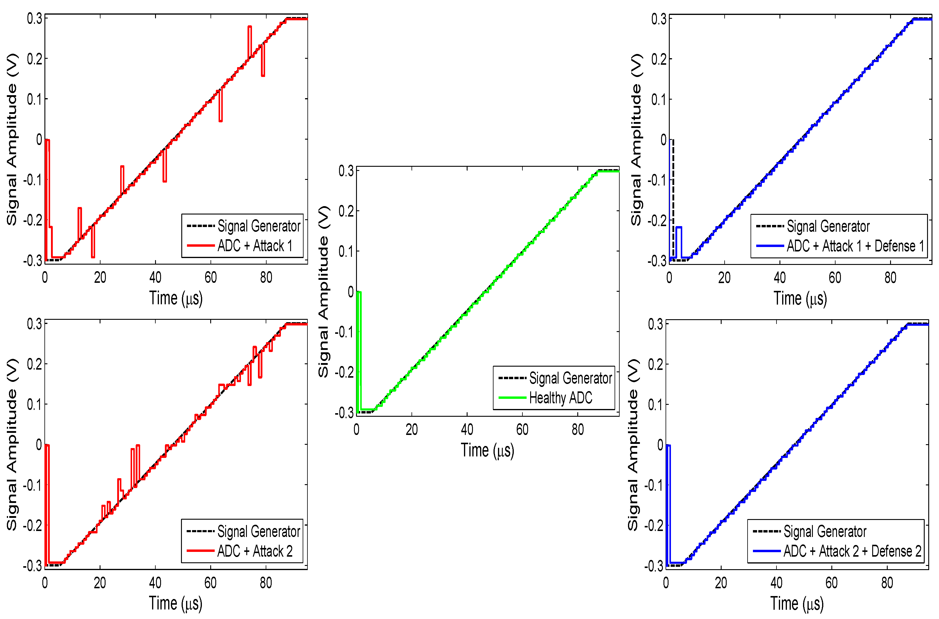
The Cadence Spectre Circuit Simulator is used for simulation and analysis of the implemented conditions for the ADC circuit. The duration time for the transient analysis is set to 120 s, the system clock signal frequency () is set to 20 MHz, the base capacitance in the SHC block is set to 20 fF, and the supply voltage is set to 0.3 V for all of the simulations run. The capacitance for each bit is a factor of the base capacitance depending on its index. For functionality evaluation, a ramp signal is applied to the ADC. A full scale ramp input signal is an ideal waveform for testing an ADC since it causes generation of all the possible codes (having 64 codes for a six-bit ADC) [35,36,37,38,39,40]. Regarding the applied ramp signal, its maximum amplitude is 0.3 V, slope starting point is at 5 s, and slope ending point is at 87 s. The simulation results for functionality evaluation of the ADC in the five operating conditions are presented in Figure 15. The magnification of the results for the second to the fifth conditions (or cases “a” to “d”) is shown in Figure 16. As the figures show, the designed Hardware Trojans demolish the ADC functionality. The datapath-based Trojan brings only spikes to the reconstructed analog signal from the ADC output, while the control-based Trojan makes large and small variations in the reconstructed signal. The defense circuits demonstrate effectiveness in eliminating the payloads of Trojans. The datapath-based countermeasure reduces even the unwanted variations in the ADC startup time.
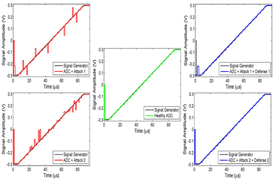
Figure 15.
The ADC functionality evaluation in five different operating conditions.
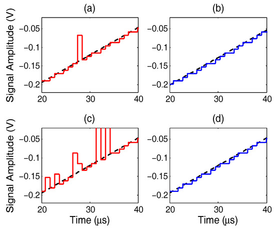
Figure 16.
The magnification (an enlarged portion) of the ADC functionality evaluation: (a) ADC + Attack 1; (b) ADC + Attack 1 + Defense 1; (c) ADC + Attack 2; and (d) ADC + Attack 2 + Defense 2.
Seven metrics are employed in order to evaluate the ADC performance in the aforementioned five conditions: (1) the total harmonic distortion (THD); (2) the effective number of bits (ENOB); (3) the root mean square (RMS) power consumption for the analog signal generator; (4) the RMS power consumption for the supply voltage; (5) the percentage of change in total area of the utilized cells; (6) the absolute value of the mean of the difference between the reconstructed analog signals from the outputs of the reference and test ADCs; and (7) the standard deviation of the adjacent differences between the reconstructed analog signals from the outputs of the reference and test ADCs. The THD metric shows the amount of present harmonic distortion, the linearity, and the quality in the ADC output. The ENOB metric is effective resolution or resolution of an ideal ADC under noise and other source of errors. It indicates the dynamic range and the accuracy of the ADC. The power metrics exhibit the ADC suitability for low power applications. The footprints of the Trojan and the defense circuits on the chip area are depicted in the fifth metric results. The sixth and the seventh metrics are used to illustrate how proximate two signals are. For all of these metrics (except ENOB), an ADC circuit has better performance if it delivers smaller values.
For obtaining these metrics, an ideal single-ended sinusoidal signal is generated and applied to the ADC, with a maximum amplitude of 0.12 V and a frequency of 20 kHz. The input signal amplitude is within the converter full-scale. This signal can provide a more realistic view of the ADC performance and functionality under the discussed operating conditions since its parameters are not in accordance with the ADC sampling condition. Let’s discuss what it means. The system clock frequency () is 20 MHz, the sampling clock frequency () is 2.5 MHz, and the converter bandwidth is 1.25 MHz, which is far greater than the input signal frequency (). The fully-differential input signal has the peak-to-peak amplitude () of 0.48 V that is compared against the fully-differential input full-scale () that is 0.6 V. The ADC sampling condition for normal operation allows a change of LSB from sample to sample and the maximum rate of change is given at zero-crossings. This condition can be formulated as , in which n is the number of ADC output bits. This condition causes reduction in the converter effective bandwidth. With substituting the values into the formula, we get , which shows the condition dissatisfaction by the chosen frequency for the input signal. Dissatisfaction of this condition can reduce the effective number of bits and increase the total harmonic distortion.
The selected window for ENOB calculation is rectangular. The ADC performance evaluation results are presented in Table 1. According to the results, the defense circuits compensate and improve the ADC degraded performance, which is caused by the Hardware Trojans. From the second to the fourth operating conditions, the large THD and the small ENOB values are due to the dissatisfaction of the sampling condition (and the payloads of the Hardware Trojans). Due to the fact that an analog to digital converter forms a nearly small portion of the overall power consumption and area occupation of a system on chip [41,42,43,44,45], the area and power overheads made by the Trojan and defense circuits are relatively low. Meanwhile, the delays caused by the datapath-based Trojan and defense circuits are around 0.2 ns and 403 ns, respectively, in this simulation analysis.

Table 1.
The analog to digital converter performance evaluation results.
4. Conclusions
This work studies a TFET-based low power six-bit SAR ADC from the security perspective. The chosen ADC is just an example, and the discussed security principles can be generalized and applied to any SAR ADC with different resolution and configuration. The datapath and the control unit of the ADC are targeted for threat and countermeasure design and development. In addition, related flowcharts are created to depict the ADC operation under the developed malicious and secure conditions. Finally, the impacts of these conditions on the ADC circuit functionality and performance are investigated. According to the results, the infected ADCs malfunction sometimes and demonstrate poor performance due to delivering less accurate and distorted output. In addition, the output smoothness is noticeably degraded. On the other hand, the defense circuits attempt to correct the ADC functionality in case of error occurrence. Furthermore, they somehow filter and smooth the ADC output. The power and area overheads caused by the Hardware Trojans as well as the defense circuits are low, considering the small possessed portion of the SoC chip by the analog to digital converter. In conclusion, it is our understanding that this work is the first attempt to analyze the security threats and countermeasures of the SAR ADC in the literature.
Acknowledgments
This work is supported in part by a seed grant from the Florida Center for Cybersecurity ().
Author Contributions
Shayan Taheri proposed the threat and countermeasure models, implemented the circuits, performed simulations, acquired and analyzed the experimental data, and wrote the manuscript. Jie Lin assisted in implementing the datapath-based threat as well as debugging the simulation issues. Jiann-Shiun Yuan provided technical feedback and reviewed the manuscript. Shayan Taheri and Jiann-Shiun Yuan read and confirmed the final version of manuscript.
Conflicts of Interest
The authors declare no conflict of interest.
References
- Wang, Q.; Geiger, R.L.; Chen, D. Hardware Trojans embedded in the dynamic operation of analog and mixed-signal circuits. In Proceedings of the 2015 IEEE National Aerospace and Electronics Conference (NAECON), Dayton, OH, USA, 15–19 June 2015; pp. 155–158. [Google Scholar]
- Deyati, S.; Muldrey, B.J.; Chatterjee, A. Targeting hardware trojans in mixed-signal circuits for security. In Proceedings of the 2016 IEEE 21st International Mixed-Signal Testing Workshop (IMSTW), Sant Feliu de Guixols, Spain, 4–6 July 2016; pp. 1–4. [Google Scholar]
- Beringuier-Boher, N.; Gomina, K.; Hely, D.; Rigaud, J.B.; Beroulle, V.; Tria, A.; Damiens, J.; Gendrier, P.; Candelier, P. Voltage glitch attacks on mixed-signal systems. In Proceedings of the 2014 IEEE 17th Euromicro Conference on Digital System Design (DSD), Verona, Italy, 27–29 August 2014; pp. 379–386. [Google Scholar]
- Tehranipoor, M.; Koushanfar, F. A survey of hardware Trojan taxonomy and detection. IEEE Des. Test Comput. 2010, 27, 10–25. [Google Scholar] [CrossRef]
- Bhunia, S.; Hsiao, M.S.; Banga, M.; Narasimhan, S. Hardware Trojan attacks: Threat analysis and countermeasures. Proc. IEEE 2014, 102, 1229–1247. [Google Scholar] [CrossRef]
- Narasimhan, S.; Du, D.; Chakraborty, R.S.; Paul, S.; Wolff, F.; Papachristou, C.; Roy, K.; Bhunia, S. Multiple-parameter side-channel analysis: A non-invasive hardware Trojan detection approach. In Proceedings of the 2010 IEEE International Symposium on Hardware-Oriented Security and Trust (HOST), Anaheim, CA, USA, 13–14 June 2010; pp. 13–18. [Google Scholar]
- Bhunia, S.; Abramovici, M.; Agrawal, D.; Bradley, P.; Hsiao, M.S.; Plusquellic, J.; Tehranipoor, M. Protection against hardware trojan attacks: Towards a comprehensive solution. IEEE Des. Test 2013, 30, 6–17. [Google Scholar] [CrossRef]
- Salmani, H.; Tehranipoor, M. Layout-aware switching activity localization to enhance hardware Trojan detection. IEEE Trans. Inf. Forensics Secur. 2012, 7, 76–87. [Google Scholar] [CrossRef]
- Ferraiuolo, A.; Zhang, X.; Tehranipoor, M. Experimental analysis of a ring oscillator network for hardware trojan detection in a 90nm ASIC. In Proceedings of the 2012 IEEE/ACM International Conference on Computer-Aided Design (ICCAD), San Jose, CA, USA, 5–8 November 2012; pp. 37–42. [Google Scholar]
- Xiao, K.; Tehranipoor, M. BISA: Built-in self-authentication for preventing hardware Trojan insertion. In Proceedings of the 2013 IEEE International Symposium on Hardware-Oriented Security and Trust (HOST), Austin, TX, USA, 2–3 June 2013; pp. 45–50. [Google Scholar]
- Karri, R.; Rajendran, J.; Rosenfeld, K.; Tehranipoor, M. Trustworthy Hardware: Identifying and Classifying Hardware Trojans. Computer 2010, 43, 39–46. [Google Scholar] [CrossRef]
- Zhang, X.; Tehranipoor, M. Case study: Detecting hardware Trojans in third-party digital IP cores. In Proceedings of the 2011 IEEE International Symposium on Hardware-Oriented Security and Trust (HOST), San Diego, CA, USA, 5–6 June 2011; pp. 67–70. [Google Scholar]
- Çakir, B.; Malik, S. Hardware Trojan detection for gate-level ICs using signal correlation based clustering. In Proceedings of the 2015 Design, Automation & Test in Europe Conference & Exhibition, EDA Consortium, Grenoble, France, 9–13 March 2015; pp. 471–476. [Google Scholar]
- Adamov, A.; Saprykin, A.; Melnik, D.; Lukashenko, O. The problem of Hardware Trojans detection in System-on-Chip. In Proceedings of the 2009 10th International Conference The Experience of Designing and Applications of CAD Systems in Microelectronics (CADSM), Lviv, Ukraine, 24–28 February 2009; pp. 178–179. [Google Scholar]
- Wang, X.; Tehranipoor, M.; Plusquellic, J. Detecting malicious inclusions in secure hardware: Challenges and solutions. In Proceedings of the 2008 IEEE International Workshop on Hardware-Oriented Security and Trust (HOST), Anaheim, CA, USA, 9 June 2008; pp. 15–19. [Google Scholar]
- Stroud, C.E. An automated BIST approach for general sequential logic synthesis. In Proceedings of the 25th ACM/IEEE Design Automation Conference, Los Angeles, CA, USA, 12–15 June 1988; pp. 3–8. [Google Scholar]
- Wu, T.F.; Ganesan, K.; Hu, Y.A.; Wong, H.S.P.; Wong, S.; Mitra, S. TPAD: Hardware Trojan prevention and detection for trusted integrated circuits. IEEE Trans. Comput. Aided Des. Integr. Circuits Syst. 2016, 35, 521–534. [Google Scholar] [CrossRef]
- Chakraborty, R.S.; Narasimhan, S.; Bhunia, S. Hardware Trojan: Threats and emerging solutions. In Proceedings of the 2009 IEEE International High Level Design Validation and Test Workshop (HLDVT), San Francisco, CA, USA, 4–6 November 2009; pp. 166–171. [Google Scholar]
- Rajendran, J.; Sinanoglu, O.; Karri, R. Regaining trust in VLSI design: Design-for-trust techniques. Proc. IEEE 2014, 102, 1266–1282. [Google Scholar] [CrossRef]
- Girard, P. Survey of low-power testing of VLSI circuits. IEEE Des. Test Comput. 2002, 19, 82–92. [Google Scholar] [CrossRef]
- Tehranipoor, M.; Wang, C. Introduction to Hardware Security and Trust; Springer Science & Business Media: Berlin/Heidelberg, Germany, 2011. [Google Scholar]
- Rostami, M.; Koushanfar, F.; Rajendran, J.; Karri, R. Hardware security: Threat models and metrics. In Proceedings of the 2013 IEEE/ACM International Conference on Computer-Aided Design, San Jose, CA, USA, 18–21 November 2013; pp. 819–823. [Google Scholar]
- Potlapally, N. Hardware security in practice: Challenges and opportunities. In Proceedings of the 2011 IEEE International Symposium on Hardware-Oriented Security and Trust (HOST), San Diego, CA, USA, 5–6 June 2011; pp. 93–98. [Google Scholar]
- Kalogeridou, G.; Sklavos, N.; Moore, A.W.; Koufopavlou, O. Security of ICs from Hardware Trojans. In Proceedings of the Workshop on Trustworthy Manufacturing and Utilization of Secure Devices, Grenoble, France, 13 March 2015. [Google Scholar]
- Yang, K.; Hicks, M.; Dong, Q.; Austin, T.; Sylvester, D. A2: Analog malicious hardware. In Proceedings of the 2016 IEEE Symposium on Security and Privacy (SP), San Jose, CA, USA, 22–26 May 2016; pp. 18–37. [Google Scholar]
- Beringuier-Boher, N.; Hely, D.; Beroulle, V.; Damiens, J.; Candelier, P. Increasing the security level of analog IPs by using a dedicated vulnerability analysis methodology. In Proceedings of the 2013 14th International Symposium on Quality Electronic Design (ISQED), Santa Clara, CA, USA, 4–6 March 2013; pp. 531–537. [Google Scholar]
- Lundberg, K.H. Analog-to-Digital Converter Testing. Massachusetts Institute of Technology: Cambridge, MA, USA, 2002. Available online: web.mit.edu/klund/www/papers/UNP_A2Dtest.pdf (accessed on 20 February 2017).
- Confalonieri, P.; Zamprogno, M.; Girardi, F. Method of Operating SAR-Type ADC and An ADC Using the Method. U.S. Patent 6,720,903, 13 April 2004. [Google Scholar]
- Lin, J.; Yuan, J.S. Ultra-Low Power Successive Approximation Analog-to-Digital Converter Using Emerging Tunnel Field Effect Transistor Technology. J. Low Power Electron. 2016, 12, 218–226. [Google Scholar] [CrossRef]
- Wang, X.; Mal-Sarkar, T.; Krishna, A.; Narasimhan, S.; Bhunia, S. Software exploitable hardware Trojans in embedded processor. In Proceedings of the 2012 IEEE International Symposium on Defect and Fault Tolerance in VLSI and Nanotechnology Systems (DFT), Austin, TX, USA, 3–5 October 2012; pp. 55–58. [Google Scholar]
- Dubeuf, J.; Hély, D.; Karri, R. Run-time detection of hardware Trojans: The processor protection unit. In Proceedings of the 2013 18th IEEE European Test Symposium (ETS), Avignon, France, 27–30 May 2013; pp. 1–6. [Google Scholar]
- Milor, L.S. A tutorial introduction to research on analog and mixed-signal circuit testing. IEEE Trans. Circuits Syst. II Analog Digit. Signal Proc. 1998, 45, 1389–1407. [Google Scholar] [CrossRef]
- Lu, H.; Ytterdal, T.; Seabaugh, A. Universal TFET Model. NEEDS: Nano-Engineered Electronic Device Simulation Node: West Lafayette, IN, USA, January 2015. Available online: https://nanohub.org/publications/31/1 (accessed on 30 January 2017). [CrossRef]
- Fan, M.L.; Chen, Y.N.; Su, P.; Chuang, C.T. Challenges and Designs of TFET for Digital Applications. In Tunneling Field Effect Transistor Technology; Springer: Berlin, Germany, 2016; pp. 89–109. [Google Scholar]
- Provost, B.; Sanchez-Sinencio, E. On-chip ramp generators for mixed-signal BIST and ADC self-test. IEEE J. Solid State Circuits 2003, 38, 263–273. [Google Scholar] [CrossRef]
- Huang, J.L.; Ong, C.K.; Cheng, K.T. A BIST scheme for on-chip ADC and DAC testing. In Proceedings of the conference on Design, Automation and Test in Europe, Paris, France, 27–30 March 2000; pp. 216–220. [Google Scholar]
- Wang, J.; Sanchez-Sinencio, E.; Maloberti, F. Very linear ramp-generators for high resolution ADC BIST and calibration. In Proceedings of the 43rd IEEE Midwest Symposium on Circuits and Systems, Lansing, MI, USA, 8–11 August 2000; Volume 2, pp. 908–911. [Google Scholar]
- Max, S. Ramp testing of ADC transition levels using finite resolution ramps. In Proceedings of the 2001 IEEE International Test Conference, Baltimore, MD, USA, 1 November 2001; pp. 495–501. [Google Scholar]
- Lee, W.T.; Liao, Y.Z.; Hsu, J.C.; Hwang, Y.S.; Chen, J.J. A high precision ramp generator for low cost ADC test. In Proceedings of the 2008 9th International Conference on Solid-State and Integrated-Circuit Technology (ICSICT), Beijing, China, 20–23 October 2008; pp. 2103–2106. [Google Scholar]
- Doernberg, J.; Lee, H.S.; Hodges, D.A. Full-speed testing of A/D converters. IEEE J. Solid State Circuits 1984, 19, 820–827. [Google Scholar] [CrossRef]
- Fossum, E.R. CMOS image sensors: Electronic camera-on-a-chip. IEEE Trans. Electron Devices 1997, 44, 1689–1698. [Google Scholar] [CrossRef]
- Saleh, R.; Wilton, S.; Mirabbasi, S.; Hu, A.; Greenstreet, M.; Lemieux, G.; Pande, P.P.; Grecu, C.; Ivanov, A. System-on-chip: Reuse and integration. Proc. IEEE 2006, 94, 1050–1069. [Google Scholar] [CrossRef]
- Eltoukhy, H.; Salama, K.; Gamal, A.E. A 0.18-/spl mu/m CMOS bioluminescence detection lab-on-chip. IEEE J. Solid State Circuits 2006, 41, 651–662. [Google Scholar] [CrossRef]
- Chae, M.S.; Liu, W.; Sivaprakasam, M. Design optimization for integrated neural recording systems. IEEE J. Solid State Circuits 2008, 43, 1931–1939. [Google Scholar] [CrossRef]
- Lee, S.C.; Jeon, Y.D.; Kwon, J.K.; Kim, J. A 10-bit 205-MS/s 1.0- mm 2 90-nm CMOS Pipeline ADC for Flat Panel Display Applications. IEEE J. Solid State Circuits 2007, 42, 2688–2695. [Google Scholar] [CrossRef]


© 2017 by the authors. Licensee MDPI, Basel, Switzerland. This article is an open access article distributed under the terms and conditions of the Creative Commons Attribution (CC BY) license (http://creativecommons.org/licenses/by/4.0/).