Article

A ZVS Bidirectional Inverting Buck-Boost Converter Using Coupled Inductors

School of Mechanical Engineering, Shanghai Jiao Tong University, Shanghai 200240, China
*
Author to whom correspondence should be addressed.
Electronics 2018, 7(10), 221; https://doi.org/10.3390/electronics7100221
Submission received: 21 August 2018 / Revised: 16 September 2018 / Accepted: 26 September 2018 / Published: 28 September 2018

Abstract

:
The bidirectional inverting buck-boost converter (BIBBC) has a simple structure and a wide voltage ratio. It can be used in the battery supercapacitor hybrid energy storage system (BSHESS) and the motor drive system. However, the traditional continuous conduction mode (CCM) BIBBC will have severe switching loss. The triangular current mode (TCM) BIBBC can reduce the switching loss, but it will increase core loss and filter capacitance. To solve these problems, this paper proposes a new zero voltage switching (ZVS) BIBBC using a coupled inductor. This ZVS BIBBC will provide ZVS conditions for both transistors whether in positive operation or negative operation. Meanwhile, this ZVS BIBBC has small core losses and filter capacitance, and can be used simply. Finally, experimental results obtained from these BIBBC experimental prototypes are presented to validate the soft-switching achieving and the efficiency improvement performance. Experimental results show that both transistors of the ZVS BIBBC achieve ZVS turn-on conditions. The efficiency of the ZVS BIBBC increased by up to 10 percent compared to the traditional CCM BIBBC at heave load, and by up to 1.5 percent compared to the TCM BIBBC at a light load.

1. Introduction

The nonisolated bidirectional DC/DC converter (NIBDC) can be used in the motor drive system and the battery supercapacitor hybrid energy storage system (BSHESS) [1,2,3,4,5]. In the BSHESS, the NIBDC is used to control the power flow between the supercapacitor and the battery. The energy management system of the BSHESS uses the NIBDC to manage and distribute the energy of the BIHESS to obtain two goals: improve battery life and increase vehicle efficiency [6,7,8]. Commonly-used NIBDCs have two types: The buck/boost converter and the buck-boost converter [9]. These NIBDCs have two operation directions: The positive operation and the negative operation. The buck/boost converter only has the voltage step-down function in positive operation, and only has the voltage step-up function in negative operation. In contrast with the bidirectional buck/boost converter, the bidirectional inverting buck-boost converter (BIBBC) has both voltage step-down and step-up functions whether in positive or negative operation. This means that the BIBBC will improve the performance of the motor drive system and the BSHESS. However, the BIBBC has higher voltage and current stress than the buck/boost converter under the same output voltage and current. Meanwhile the traditional continuous conduction mode (CCM) BIBBC works under hard-switching conditions. These factors introduce serious conducting and switching losses. To improve the efficiency of the BIBBC, the soft-switching technique is required.
For the BIBBC, one of switches can always obtain the soft-switching condition. Therefore the key is the soft-switching condition for another switch. The simplest soft-switching technology for the BIBBC is the triangular current mode (TCM) method [10], which provides soft-switching conditions for both switches by adjusting the value of the main inductor L. This technology does not use any auxiliary circuitry. However with this technology, the inductor current iL has large current ripples, which will introduce large current stresses, large core losses, and a large filter capacitance. In order to overcome these shortcomings, many new soft-switching technologies are proposed.
The zero voltage transition (ZVT) technology is a commonly used method for the BIBBC [11,12,13,14,15,16]. By adding auxiliary switches, the ZVT technology gives zero voltage switching (ZVS) conditions for the main switches and zero current switching (ZCS) conditions for the auxiliary switches. Some improved ZVT methods use a coupled inductor to reduce core numbers and improve soft-switching performance [11,13,15]. ZVT-based topologies have high efficiency. The main shortcoming is the cost of auxiliary switches and the complex control timing, because the soft-switching condition is dependent on the control timing. The active clamped soft-switching technology was proposed in multiple previous papers [17,18] for the buck/boost converter, and this technology can also be used in the bidirectional buck-boost converter. In this method only one auxiliary switch is used to obtain soft-switching conditions for two main switches. The coupled inductor can also be used in this topology to improve performance [18]. The shortcoming of these active clamped topologies is the cost of auxiliary switches and the complex control timing. In order to reduce the control complexity of soft-switching topologies, some soft-switching technologies without auxiliary switches were proposed previously [19,20]. In these topologies, the auxiliary circuit, composed of inductors and capacitors, is introduced to the BIBBC to obtain soft-switching conditions. These topologies have a simple structure and have no auxiliary switches. However a previously proposed method is based on the special application (battery equalization applications) [19], and another previously proposed method also faces the problem of large current stresses and core losses [20].
For the existing soft-switching BIBBCs, TCM BIBBCs introduces large current stresses, large core losses, and large filter capacitance; ZVT BIBBCs need auxiliary switches and complex control timing. To overcome these shortcomings, this paper proposes a new ZVS BIBBC using a coupled inductor based on the buck-boost converter in literature [21,22], in which the converter can only obtain soft-switching conditions in positive operation. The structural difference between the proposed ZVS BIBBC and the original converter is the introduced diode. With this diode the ZVS BIBBC has a different operation principle to the original converter, and can provide soft-switching conditions for both transistors whether in positive operation or negative operation. The proposed ZVS BIBBC has comprehensive advantages over similar existing converters:
  • Higher efficiency than the CCM BIBBC in most power ranges and higher efficiency than the TCM BIBBC in the medium and low power range;
  • A simpler control method and lower cost than ZVT converters;
  • Lower core losses and filter capacitance than the TCM BIBBC.
  • In short, this paper provides the following contributions:
  • Proposal of a new ZVS BIBBC using a coupled inductor with abovementioned advantages;
  • Detailed theoretical analysis and design guidelines of the new ZVS BIBBC;
  • Experimental analysis and comparison between the proposed ZVS BIBBC and two other BIBBCs.
This paper is organized as follows. Section 2 presents the topology description and operating principle; the soft-switching achieving condition, stress and loss analysis, and design guidelines are given in Section 3. Experimental results and the related analysis are presented in Section 4. Section 5 summarizes the content and contributions of the full paper.

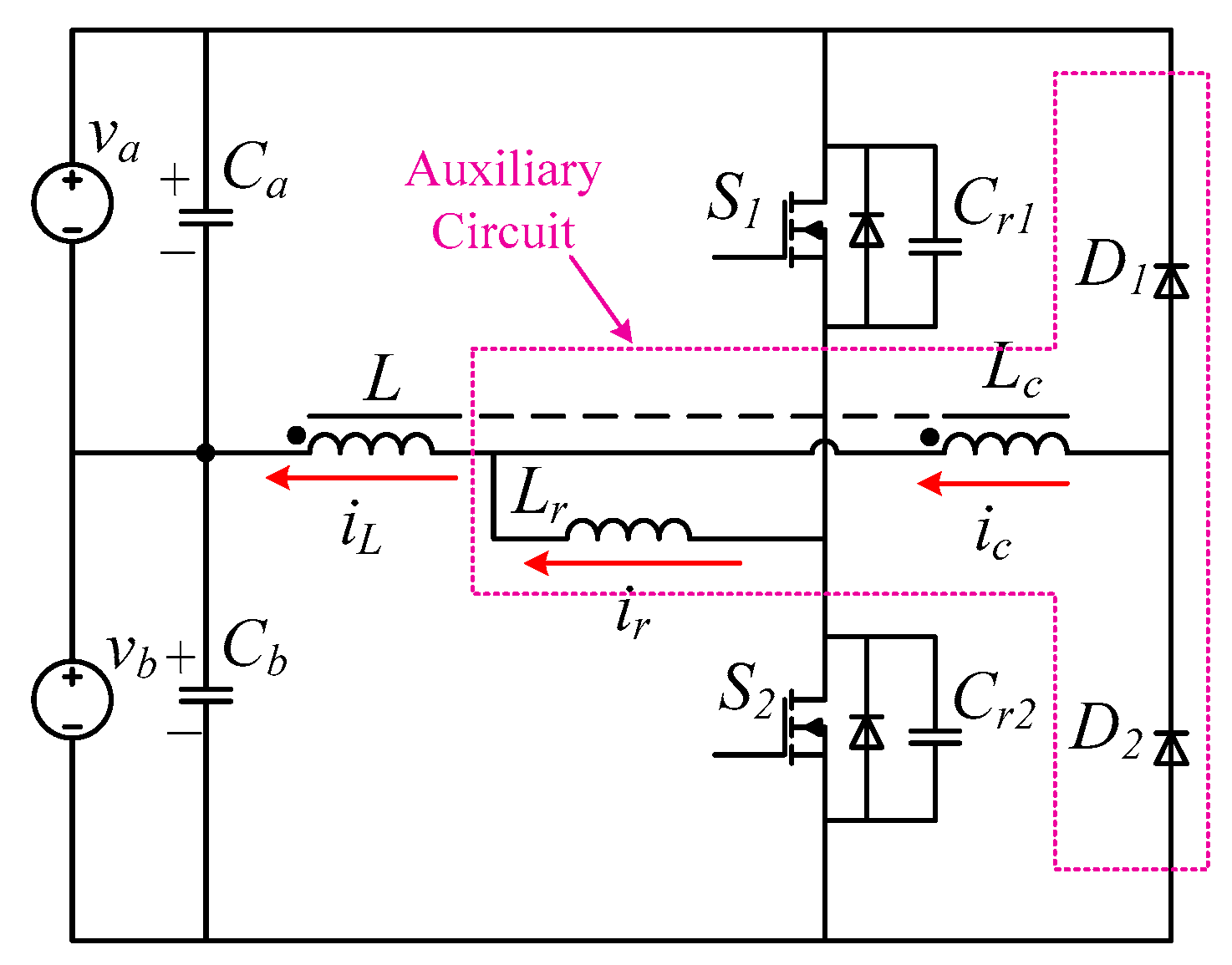
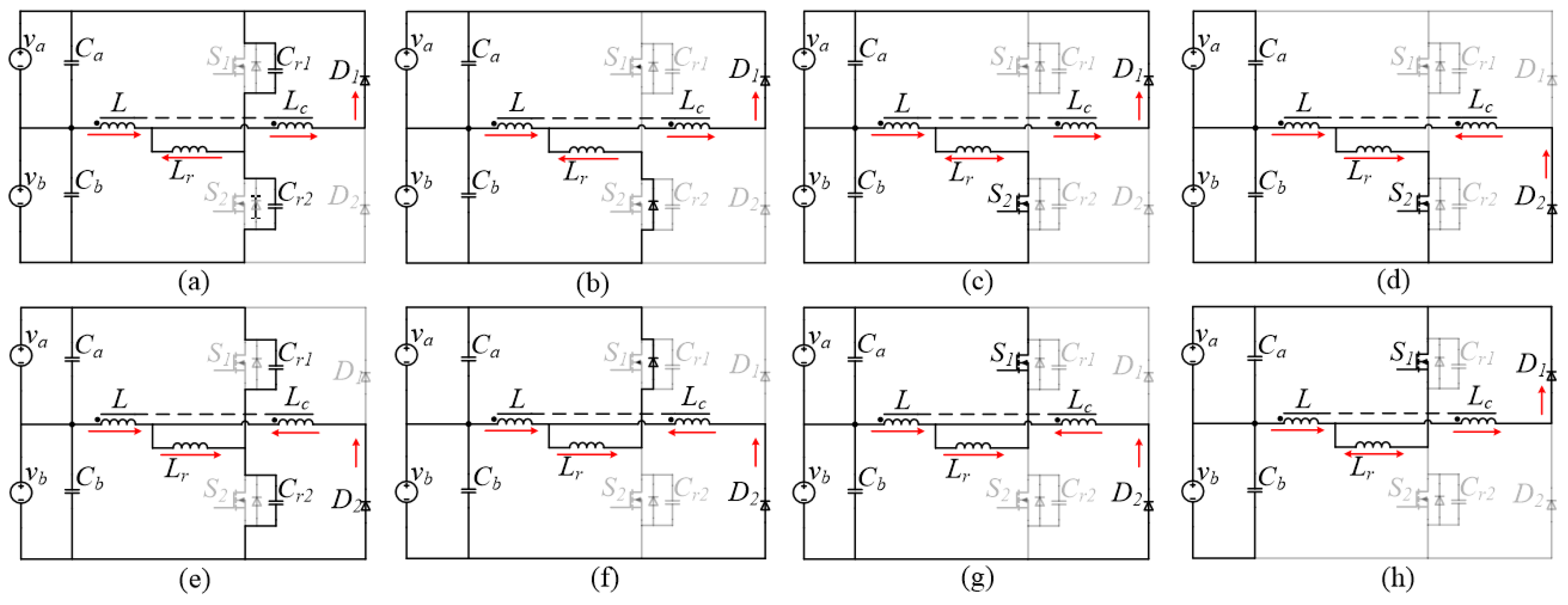
2. Topology and Its Principle

2.1. Proposed Converter

The proposed new ZVS BIBBC, which has bidirectional soft-switching capability, is shown in Figure 1. This converter does not use an auxiliary switch and, therefore, the control complexity of the new ZVS BIBBC is the same as a traditional CCM BIBBC. This converter is suitable for nonisolated bidirectional DC/DC applications requiring wide voltage ratios. The drawback of the proposed new ZVS BIBBC is the additional loss caused by auxiliary diodes. Nonetheless, the achieving of soft-switching conditions will improve the efficiency comparing to the hard-switching BIBBC. The proposed ZVS BIBBC also has two operation directions: The positive operation and the negative operation. In positive operation, the power flow is transferred from va to vb. In negative operation, the power flow is transferred from vb to va. As shown in Figure 1, the soft-switching auxiliary circuit of the proposed BIBBC includes two power diodes, D1 and D2, a coupled inductor Lc, and a resonance inductor Lr. The main circuit of the new ZVS BIBBC includes two transistors S1 and S2, a main inductor L, two snubber capacitors Cr1 and Cr2, and two filter capacitors Ca and Cb. Cr1 and Cr2 are connected to transistors S1 and S2 in parallel, respectively. Lr is used to compensate negative effects of Cr1 and Cr2 on ZVS-on conditions. The coupled inductor Lc, and auxiliary diodes D1 and D2 will provide ZVS-on conditions for S1 (the positive operation) and S2 (the negative operation). Other symbols are defined as follows. va and vb are the DC voltage values, ic is the current across Lc, iL is the current across L, and ir is the current across L.
In the following sections, the mathematical model of the new ZVS BIBBC will be presented. All variables are International System of Units. Based on the circuit conduction state of the ZVS BIBBC, the proposed ZVS BIBBC will have four operation intervals by ignoring the charging and discharging process of snubber capacitors. Equivalent circuits of these intervals are shown in Figure 2. These equivalent circuits can be used to build the mathematical model of the new ZVS BIBBC. For Interval I, the differential equations of currents (ic, iL, and ir) are
{ k L 1 = d i L d t = v a ( M L r ) v b ( L c + M ) ( L + M ) ( L r M ) + ( L c + M ) ( L + L r ) k c 1 = d i c d t = v a ( L + L r ) + v b ( L + M ) ( L + M ) ( L r M ) + ( L c + M ) ( L + L r ) k r 1 = d i r d t = v a ( L + M ) v b ( L + L c + 2 M ) ( L + M ) ( L r M ) + ( L c + M ) ( L + L r )  
where M is the mutual inductance between L and Lc. If k is the coupling coefficient, then M2 = k2LLc.
For Interval II, they are
{ k L 2 = d i L d t = v b ( L c + L r ) ( L + M ) ( L r M ) + ( L c + M ) ( L + L r ) k c 2 = d i c d t = v b ( M L r ) ( L + M ) ( L r M ) + ( L c + M ) ( L + L r ) k r 2 = d i r d t = v b ( L c + M ) ( L + M ) ( L r M ) + ( L c + M ) ( L + L r )  
For Interval III, they are
{ k L 3 = d i L d t = v a ( L c + M ) + v b ( M L r ) ( L + M ) ( L r M ) + ( L c + M ) ( L + L r ) k c 3 = d i c d t = v a ( L + M ) v b ( L + L r ) ( L + M ) ( L r M ) + ( L c + M ) ( L + L r ) k r 3 = d i r d t = v a ( L + L c + 2 M ) + v b ( L + M ) ( L + M ) ( L r M ) + ( L c + M ) ( L + L r )  
For Interval IV, they are
{ k L 4 = d i L d t = v a ( L c + L r ) ( L + M ) ( L r M ) + ( L c + M ) ( L + L r ) k c 4 = d i c d t = v a ( M L r ) ( L + M ) ( L r M ) + ( L c + M ) ( L + L r ) k r 4 = d i r d t = v a ( L c + M ) ( L + M ) ( L r M ) + ( L c + M ) ( L + L r )  

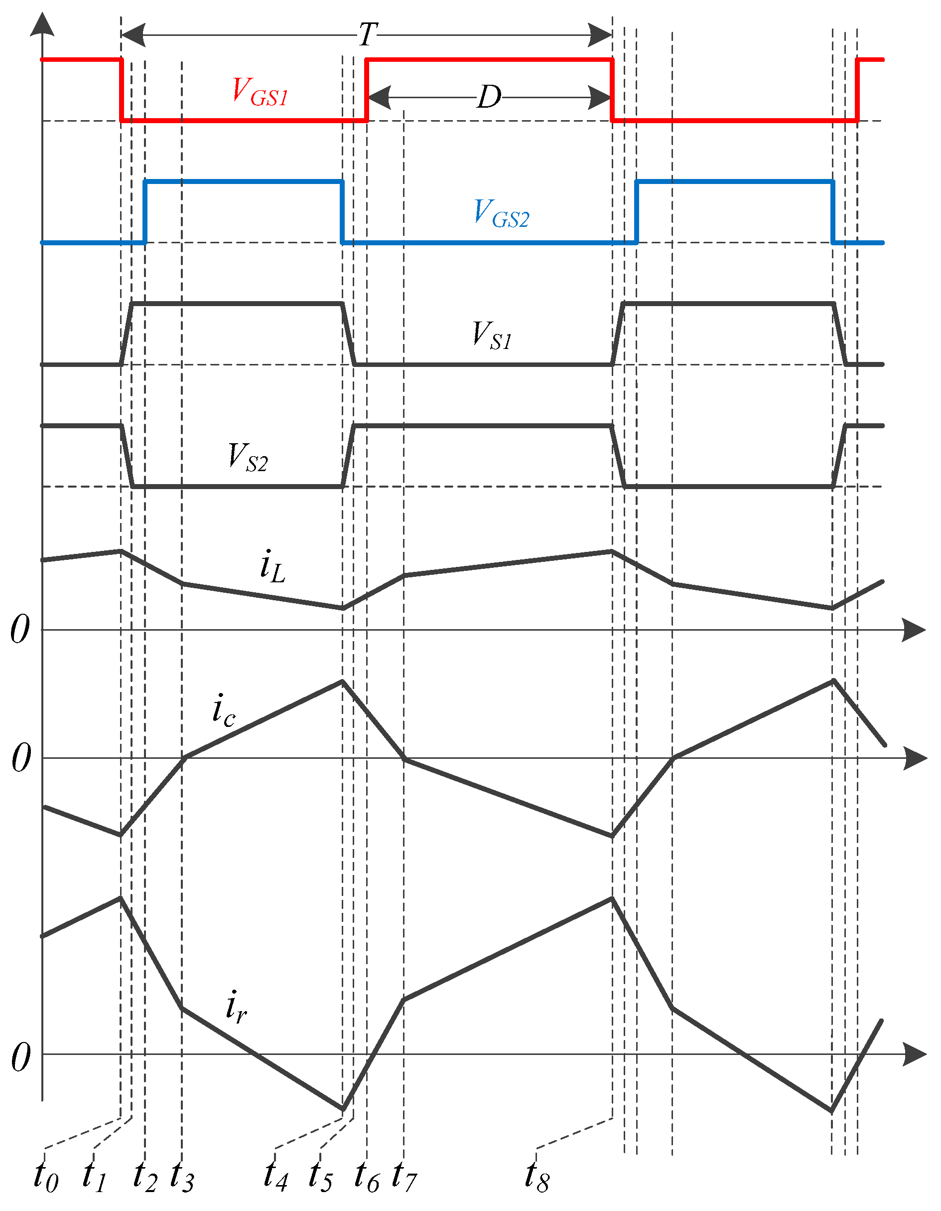
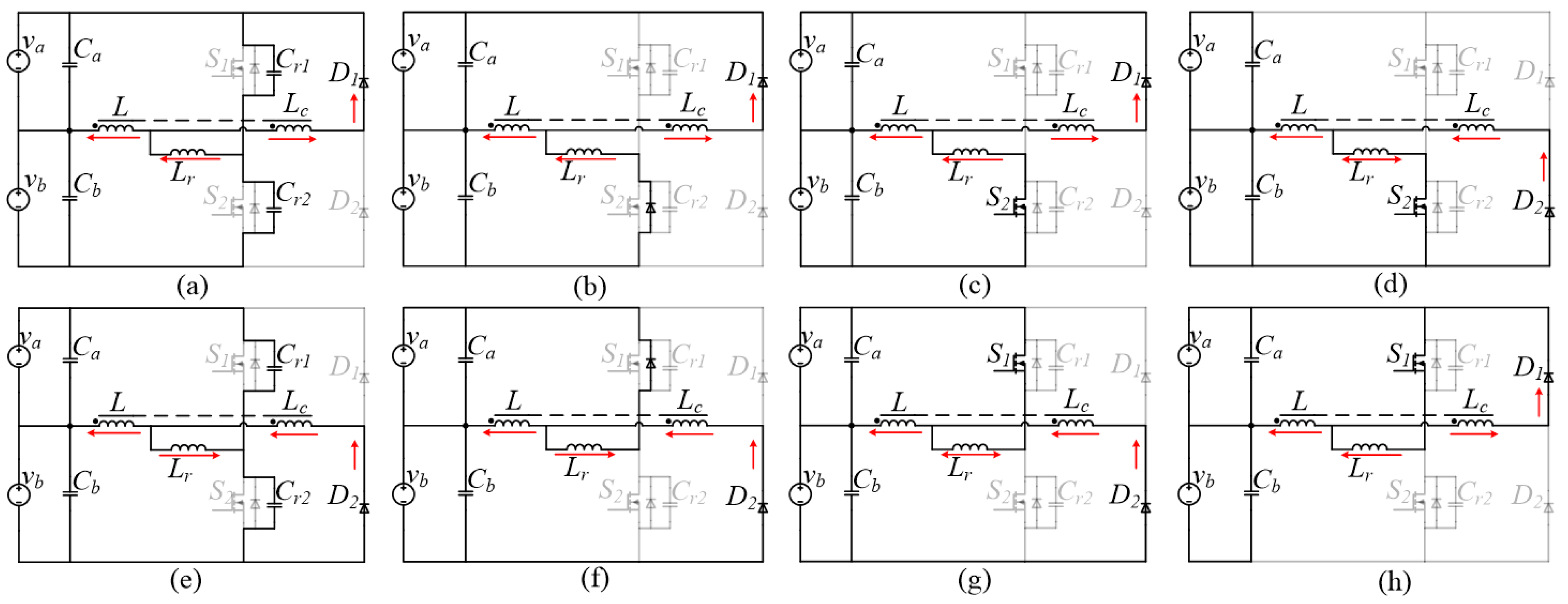
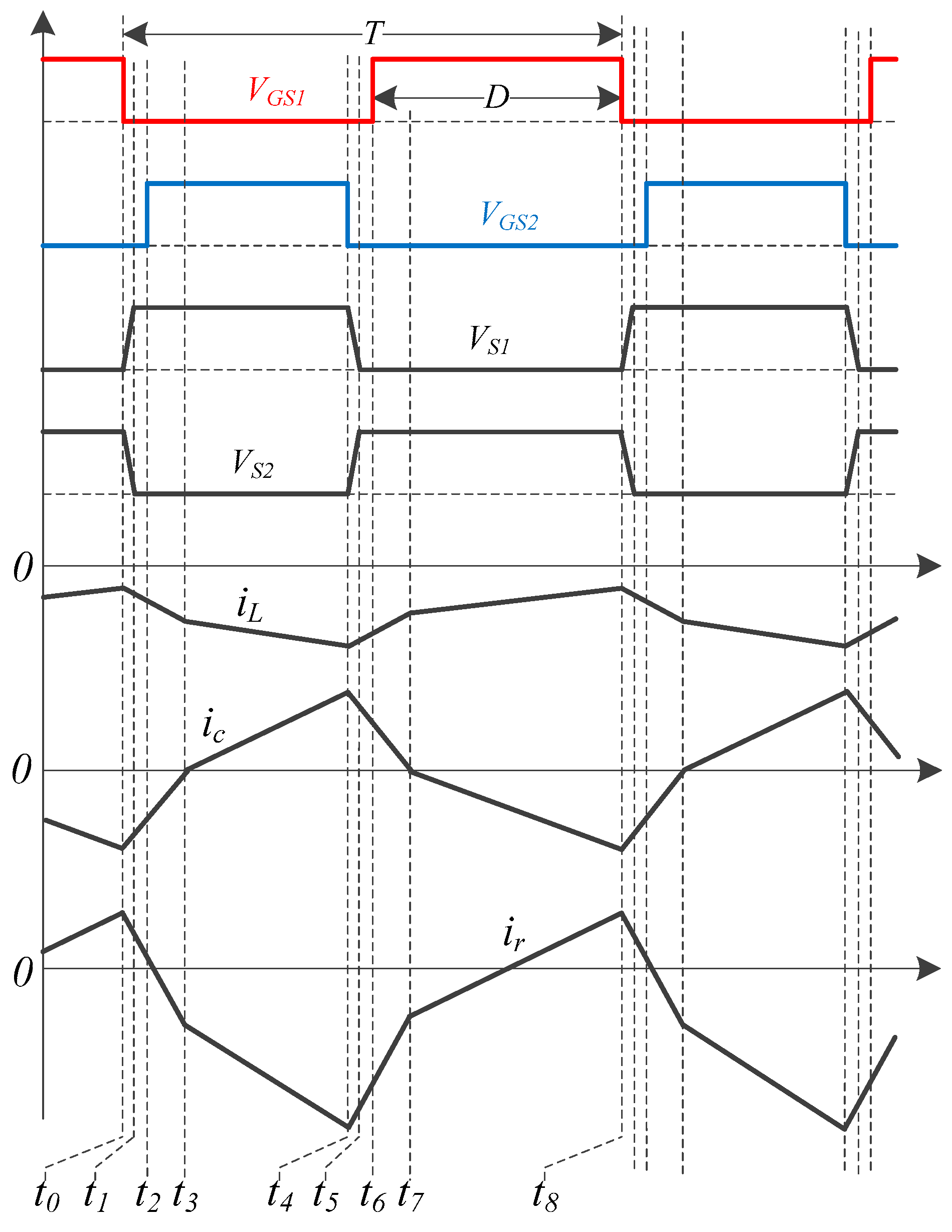
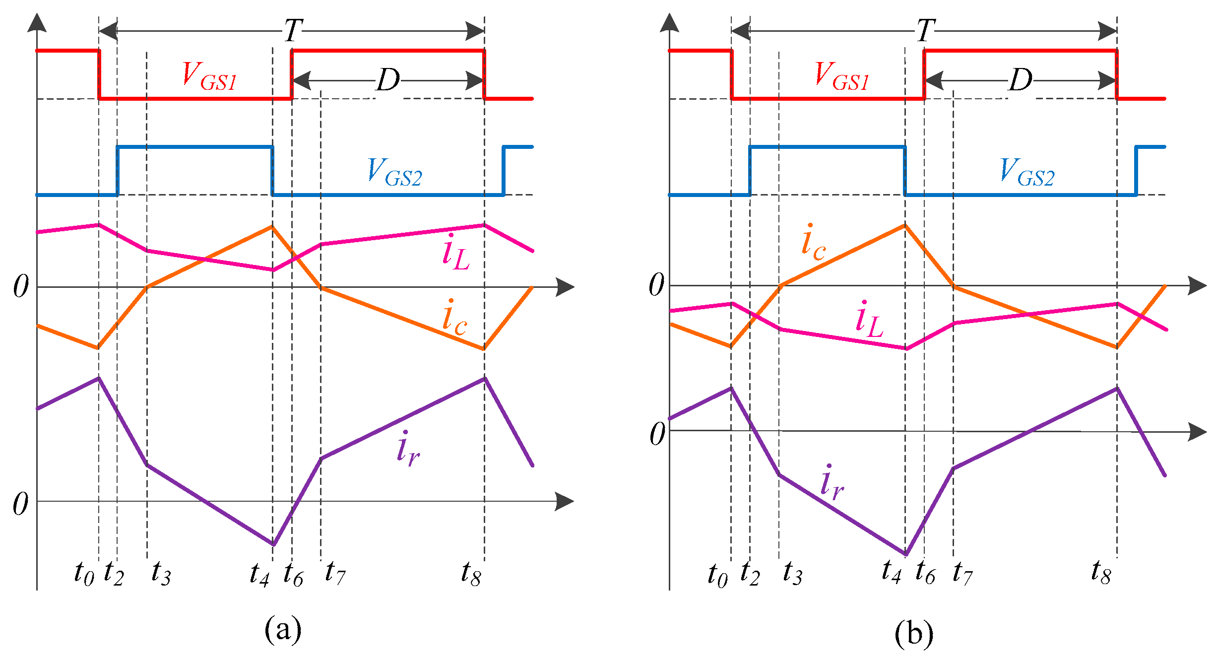
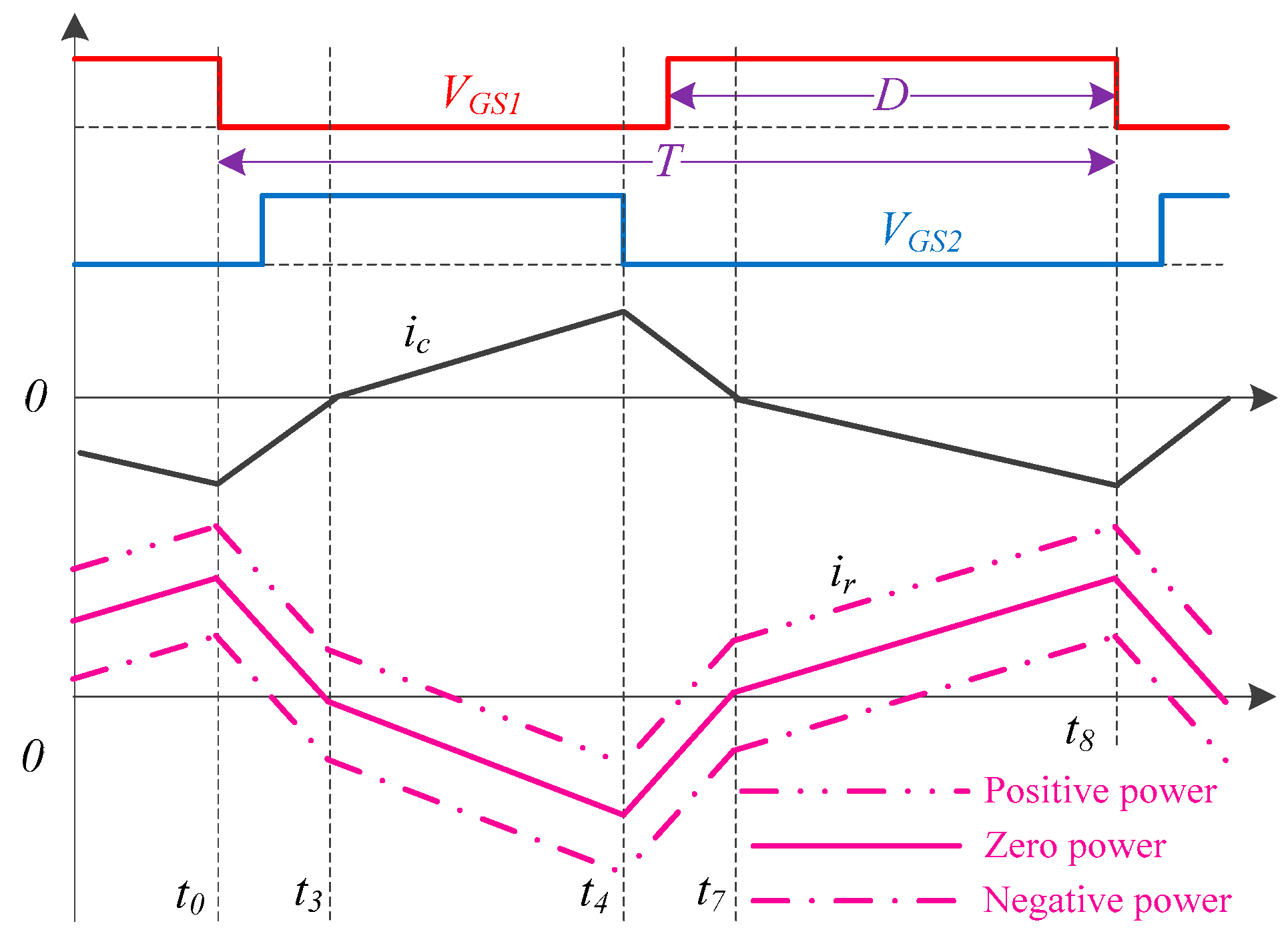
2.2. Positive Operation

To describe the operation principle clearly, this section gives the analysis of voltage and current waveforms in one switching period (T) of the positive operation. As shown in Figure 3 and Figure 4, the voltage and current waveforms of the proposed ZVS BIBBC can be divided into eight modes based on the circuit conduction state. Figure 3 gives gate signal waveforms (VGS1 and VGS2) and drain-source voltage waveforms (VS1 and VS2) respectively for S1 and S2, and also gives main current waveforms (iL, ir, and ic). In Figure 3, D is the duty cycle of the gate signal (VGS1) of S1. Figure 4 gives circuit conduction states of these modes. In positive operation, the mean value of iL will be positive, and the energy is transferred from va to vb. If the load current is large enough (all waveforms of iL are above the time-axis), iL will be continuous. D1 and D2 will not conduct at the same time. ir will be bidirectional in DT and (1 − D)T will provide soft-switching conditions for S1 and S2. The detailed analysis of each mode is presented as follows.
Mode 1 (t0–t1, Figure 4a): At the beginning of this mode (t0), S1 is turned off by the low-level of VGS1. After t0 the changing of VS1 and VS2 is slow due to the existence of Cr1 and Cr2. The ZVS-off condition of S1 is obtained. iL and ir are positive and start to decrease. ic is negative and starts to increase.
Mode 2 (t1–t2, Figure 4b): In this mode VS2 decreases to 0 at t1, and then is kept to 0 due to the conduction of the body diode of S2.
Mode 3 (t2–t3, Figure 4c): Because VS2 is 0 at t2, S2 conducts at ZVS-on condition. In this mode the changing trend of waveforms of iL, ir, and ic is same to Mode 1 and Mode 2.
Mode 4 (t3–t4, Figure 4d): At t3, the current across D1 decreases to 0, and then D1 turns off. The current across D2 starts to increase from 0, therefore, D2 turns on. ic is crossing the time-axis and become positive. The increasing rate of ic slows. The decreasing rate of iL and ir also decrease. When ic is equal to iL, ir starts to be negative.
Mode 5 (t4–t5, Figure 4e): S2 is turned off at the beginning of this mode (t4). Similar to mode 1, the changing of VS1 and VS2 is also slow. The ZVS-off condition for S2 is achieved. After t4, iL and ir start to increase. ic starts to decrease.
Mode 6 (t5–t6, Figure 4f): VS1 decreases to 0 at t5, and is clamped to 0 due to the conduction of the body diode of S1. iL, ic, and ir have the same state as Mode 5.
Mode 7 (t6–t7, Figure 4g): Because VS1 is kept at 0, S1 starts to conduct at the ZVS-on condition at t6. When ic is equal to iL, ir starts to become positive. The conducting state in this mode is the same as Mode 6.
Mode 8 (t7–t8, Figure 4h): At t7, the current across D2 decreases to 0, and then D2 turns off. And the current across D1 starts to increase from 0, therefore, D1 turns on. ic is crossing the time-axis and becomes negative. The decreasing rate of ic reduces. The rising rate of iL and ir also reduce.

2.3. Negative Operation

Similar to the positive operation, the negative operation also has eight modes. Figure 5 presents the key voltages and current waveforms, and Figure 6 presents the circuit conductive states of the negative operation. Comparing the negative operation to the positive operation, the mean value of iL is negative, and the energy will be transferred to va. ic of the negative operation has the same state as the positive operation. ir moves to the negative direction compared to the positive operation. Therefore, the zero crossing position of ir (mode 3 and mode 8) is different from the positive operation (mode 4 and mode 7). A detailed mode analysis of the negative operation can refer the mode analysis of the positive operation in Section 2.2.

3. Converter Analysis and Design

3.1. Soft-Switching Conditions

The introduction of Cr1 and Cr2 can reduce the rising rate of VS1 and VS2 to provide passive ZVS-off conditions for S1 and S2. But the existence of Cr1 and Cr2 has an adverse effect on achieving ZVS-on conditions. Therefore, the resonant inductor Lr is used to compensate the capacitive feature of switches (S1 and S2) introduced by Cr1 and Cr2. Based on the capacitor and inductor energy storage formula [23], the compensation energy formula is
( C r 1 + C r 2 ) ( v a + v b ) 2 2 = L r i r 2 2  
Based on the above operation mode analyses, soft-switching conditions of the proposed ZVS BIBBC are shown in Figure 7. Figure 7a is the ZVS-on condition for the positive operation. In positive operation, S2 will always obtain the ZVS-on condition. The ZVS-on condition of S1 is that ir must be negative at t6. Figure 7b is the ZVS-on condition for the negative operation. In negative operation, S1 will always obtain the ZVS-on condition. The ZVS-on condition of S2 is that ir must be positive at t2. Then the soft-switching conditions of the proposed BIBBC are that ir must be negative at t6 and be positive at t2.
Then soft-switching achieving equations are
at   t 6 :   i r = i L i c < 0 at   t 2 :   i r = i L i c > 0
iave is set as the average value of iL, iL is marked as iL6 at t6, and iL is marked as iL2 at t2. iave can be used to represent the load level of the new ZVS BIBBC. Because iave will be roughly equal to the median value of iL, iL can be estimated by
{ i L 6 = i a v e + k L 1 ( t 3 t 0 ) + k L 2 ( t 4 t 3 ) 2 + k L 3 ( t 6 t 4 ) i L 2 = i a v e + k L 3 ( t 7 t 4 ) + k L 4 ( t 8 t 7 ) 2 + k L 1 ( t 2 t 0 )  
At t6, ic is marked as ic6, and at t2, ic is marked as ic2, then ic will be
{ i c 6 = k c 2 ( t 4 t 3 ) + k c 3 ( t 6 t 4 ) i c 2 = k c 4 ( t 8 t 7 ) + k c 1 ( t 2 t 0 )  
Substituting (7) and (8) into (6),the soft-switching achieving equations can be rewritten as
at   t 6 :   i a v e + k L 1 ( t 3 t 0 ) + ( k L 2 2 k c 2 ) ( t 4 t 3 ) 2 + ( k L 3 k c 3 ) ( t 6 t 4 ) < 0 at   t 2 :   i a v e + k L 3 ( t 7 t 4 ) + ( k L 4 2 k c 4 ) ( t 8 t 7 ) 2 + ( k L 1 k c 1 ) ( t 2 t 0 ) > 0
To guarantee the achieving of ZVS-on conditions, the first equation of (9) limits the maximum value of the positive load (the maximum value of iave is positive), and the second equation of (9) limits the maximum value of the negative load (the minimum value of iave is negative). Equation (9) is the initial soft-switching achieving condition of the proposed converter. Because values of the time in (9) are unknown, Equation (9) cannot be used in the actual design. To further simplify (9), setting d1 = t3t0, d2 = t4t3, d3 = t7t4, d4 = t8t7, x1= d1/(d1 + d2), x2= d3/(d3 + d4). Then
{ d 1 + d 2 = ( 1 D ) T d 3 + d 4 = D T  
In one period, the changing of ir and ic is zero. Then
{ k r 1 d 1 + k r 2 d 2 + k r 3 d 3 + k r 4 d 4 = 0 k c 2 d 3 + k c 3 d 3 = 0 k c 1 d 1 + k c 4 d 4 = 0  
Based on (10) and (11), x1 and x2 are
{ x 1 = D ( M L r ) L + M x 2 = ( 1 D ) ( M L r ) L + M  
Based on (9) and (10), the soft-switching achieving equation can be rewritten as
i a v e + T ( 1 D ) [ k L 1 x 1 + ( k L 2 2 k c 2 ) ( 1 x 1 ) ] 2 + ( k L 3 k c 3 ) t d e < 0 i a v e + D T [ k L 3 x 2 + ( k L 4 2 k c 4 ) ( 1 x 2 ) ] 2 + ( k L 1 k c 1 ) t d e > 0
tde is the dead time, tde = t6t4 = t2t0. Then substituting (1)–(4), and (12) into (13), the soft-switching achieving condition is
2 ( i a v e + k r 3 t d e ) T v b ( 1 D ) < ( 1 2 D ) ( M L r ) 2 + ( L + M ) ( L c + 2 M L r ) ( L + M ) [ ( L + M ) ( L r M ) + ( L c + M ) ( L + L r ) ] 2 ( i a v e + k r 1 t d e ) D T v a > ( 1 2 D ) ( M L r ) 2 ( L + M ) ( L c + 2 M L r ) ( L + M ) [ ( L + M ) ( L r M ) + ( L c + M ) ( L + L r ) ]
Equation (14) is the soft-switching limited condition. From (14), we can determine that this equation limits the range of iave from the negative value to the positive value. The negative value of iave represents the negative power flow, and the positive value of iave represents the positive power flow. This soft-switching limited condition gives a load limiting soft-switching condition. For a designed converter, if the absolute value of iave is smaller than the designed iave, the soft-switching conditions will always be obtained. We can also know that a large Lc and small L is beneficial to achieving ZVS-on. However a small L will lead to large current ripples of iL. Therefore, Lc is the best parameter to adjust the soft-switching range.

3.2. Stress and Losses Analysis

In the proposed ZVS BIBBC, no extra voltage stress is introduced by auxiliary circuits. However the BIBBC has higher voltage stress than the buck/boost converter. The maximum voltage of main semiconductor devices (S1, S2, D1, and D2) is va + vb in both the traditional buck-boost converter and the proposed converter. Figure 8 shows the current stress analysis for S1, S2, D1, and D2. Due to the soft-switching requirement, ir crosses the 0-axis two times in one period, and has large ripples. These large ripples give the S1 and S2 of the proposed BIBBC larger current stress than the traditional CCM BIBBC. In zero-power condition, S1 and S2 have minimum current stress, and the current stress increases with increasing output power (whether positive power or negative power). In the maximum transmission power, S1 and S2 have maximum current stress. In this condition, the maximum absolute value of ir is
i r p p = D T v a ( 2 M + L c L r ) ( L + M ) ( L r M ) + ( L c + M ) ( L + L r )  
ic determines the current stress of D1 and D2. The maximum current values for D1 and D2 are
i c p 1 = v b T ( 1 D ) ( M L r ) [ L + L r + D M D L r ] ( L + M ) [ ( L + M ) ( L r M ) + ( L c + M ) ( L + L r ) ] i c p 2 = v b T ( 1 D ) ( M L r ) ( L + M + D L r D M ) ( L + M ) [ ( L + M ) ( L r M ) + ( L c + M ) ( L + L r ) ]
The loss of the proposed converter includes three parts: the on-loss and switching loss for S1 and S2, the auxiliary circuit loss, and the core loss. Thanks to the achieving of ZVS-on and ZVS-off conditions for S1 and S2, the turn-on loss is eliminated and the turn-off loss is reduced. The on-loss is larger than the traditional CCM BIBBC due to the existence of large ripples of ir. The auxiliary circuit loss is caused by diodes D1 and D2, and can be reduced using low forward voltage diodes. The core loss is related to the current ripple and the core material. In the proposed converter, ic and ir both have large ripples. So to reduce core losses, low-loss cores should be used. By rational design, the switching loss and the core loss will be reduced by the soft-switching achieving and the use of low loss cores. So for the proposed BIBBC, the conduction loss (the on-loss of S1 and S2, the on-loss of D1 and D2) is dominant.

3.3. Design Guidelines

Equation (14) can be used in the actual soft-switching design of the proposed BIBBC. iave can represent the load level of the BIBBC. It is known from (14) that the maximum absolute value of iave can be used to design the soft-switching converter. Thus soft-switching conditions can be guaranteed when the absolute value of iave is smaller than the design value. According to the above soft-switching condition analysis, the design steps are presented:
Step 1: Determine the voltage level (va, vb) and the load level (maximum absolute value of iave) according to the application environment and the stress analysis in Section 3.2. Then
D = | v b | | v a | + | v b |  
Step 2: Snubber capacitors (Cr1, Cr2) are used to reduce the increasing rate of drain-source voltages (VS1, VS2) to obtain ZVS-off conditions. Based on the increasing time and the voltage level, Cr1 and Cr2 can be selected. Lr is the resonant inductor, which is used to compensate the snubber capacitors (Cr1, Cr2). Lr can be designed based on (5).
Step 3: Current ripples of iL can be calculated based on
i L p p = v a D T L + M ( M L r ) 2 + ( L c + L r ) ( L + M ) ( L + M ) ( L r M ) + ( L c + M ) ( L + L r )  
If ignoring the magnetic coupling effect, the current ripple equation will be
i L p p = v a D T L + L r  
Then, based on the ripple requirement of iL, the initial value of L can be calculated by (19).
Step 4: Equation (14) is the soft-switching achieving condition. Based on the above calculation, all parameters except Lc and M are known. Considering k = 0.7, substituting the positive maximum value of iave in the first equation of (14), and substituting the negative minimum value of iave in the second equation of (14), Lc and M can be calculated.
Step 5: Based on (18), the final value of L can be calculated.

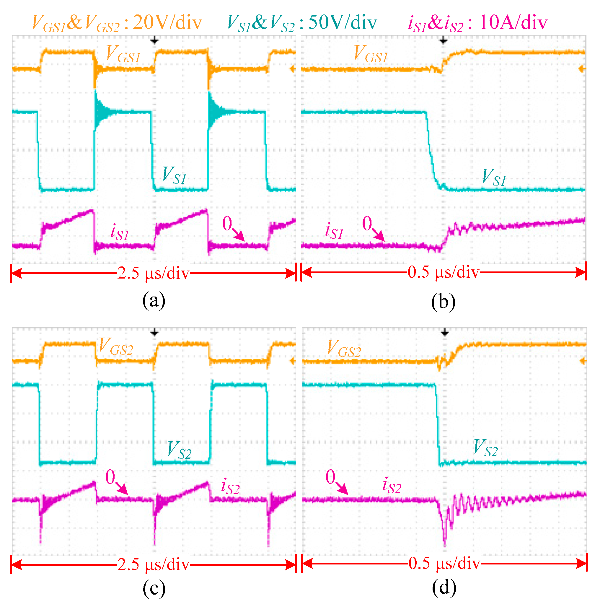
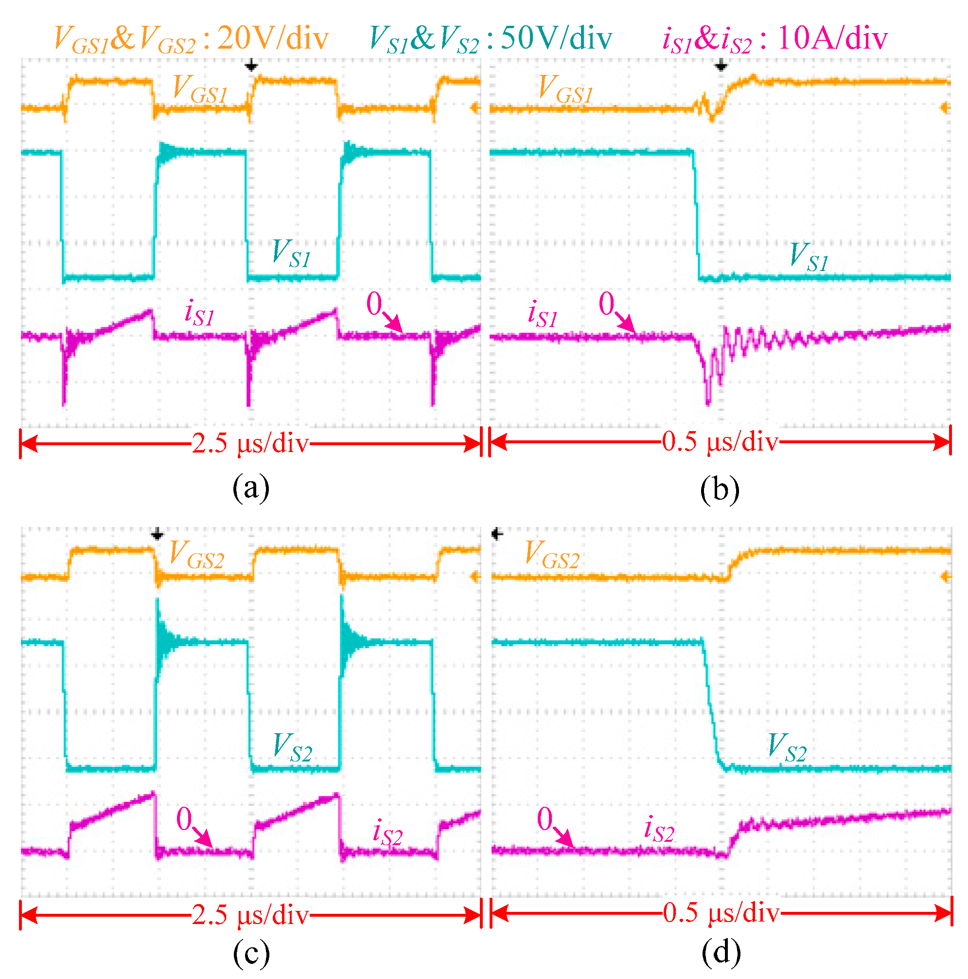
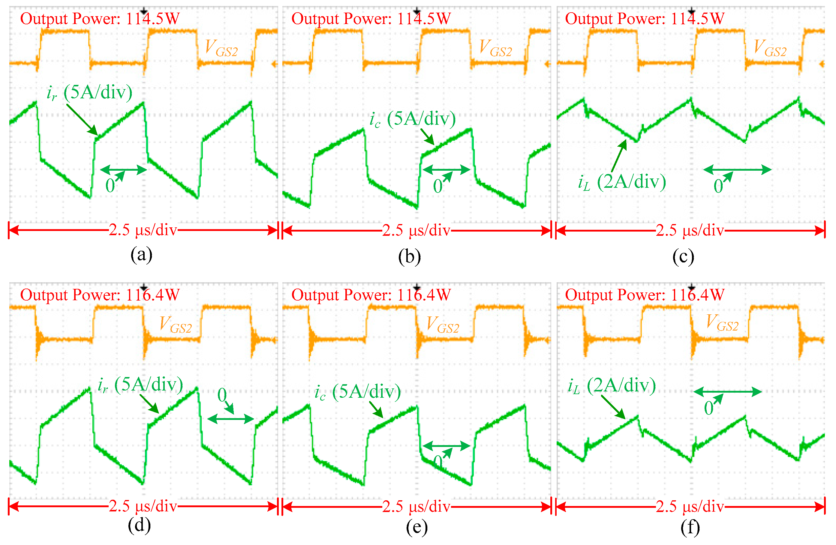
4. Experimental Results

4.1. Experimental Setup

In this section, a 200 W experimental prototype was built to illustrate the features and benefits of the proposed BIBBC. The experimental platform is composed of the experimental prototype, the control signal generator (a XC2267M board, Qianqin Technology, Beijing, China), the DC voltage source, the resistive load, and measuring tools, as shown in Figure 9. The main experimental parameters of the components of the experimental prototype are presented in Table 1. This experimental platform uses the open-loop method to test the experimental prototype in the voltage level of 70 V to 70 V. Switching waveforms of main voltages and currents are measured by voltage probes, current probes (CP8150A and CP9012S by CYBERTEK, ShenZhen ZhiYong Electronics Co., Ltd., Shenzhen, Guangdong, China), and by oscilloscope (TDS 2024C by Tektronix, Tektronix, Inc., Beaverton, OR, USA). The efficiency is measured by the power analyzer Yokogawa WT1800 (Yokogawa Test & Measurement, Musashino-shi, Tokyo, Japan). These measuring tools have appropriate precisions to reduce the effect of measurement errors on the experimental results. To prove the superiority of the proposed converter, efficiency measurement results are compared to a traditional BIBBC respectively with CCM and TCM.

4.2. Results Analysis

Soft-switching achieving: Switching waveforms of the main switches (S1 and S2) are presented in Figure 10 and Figure 11. Figure 10 shows the switching waveforms of VGS1, VGS2, VS1, VS2, iS1, and iS2 in positive operation. From these waveforms, it can be seen that the PWM gate signal VGS1 rises to a high level after VS1 decreases to 0. The ZVS turn-on condition of S1 is obtained. Similar to the switching waveforms of S1, VGS2 also rises to a high level after VS2 decreases to 0. The ZVS condition of S2 is also obtained. Figure 11 shows the switching waveforms for S1 and S2 in negative operation. ZVS conditions for S1 and S2 were also obtained based on the same analysis method. Based on these experimental waveforms, the proposed converter provides ZVS turn-on conditions for both S1 and S2, whether in positive operation or negative operation. These waveforms are measured at an output power of approximately 115 w.
Current waveforms: To prove the current waveform analysis in Section 2, current waveforms of ir, ic, and iL were measured as shown in Figure 12. We can see that iL is continuous and has a lower ripple than ir and ic. ic is composed of currents in D1 and D2. Because D1 and D2 will not conduct at the same time, the current in D1 and D2 can be obtained from ic. ir has larger ripples, which are used to provide soft-switching conditions. These waveforms are consistent with the analysis shown in Figure 3 and Figure 5.
Efficiency comparison: The measured efficiency of the proposed BIBBC is presented in Figure 13. It is compared with a traditional BIBBC with regard to CCM and TCM. The CCM BIBBC has the same L as the proposed BIBBC, and it works under hard-switching conditions. The value of L in the TCM BIBBC is 18.95 μH, and it works under soft-switching conditions. From these efficiency curves in Figure 13, the proposed BIBBC and the TCM BIBBC have higher efficiency than the CCM BIBBC in most output power range. The proposed BIBBC has a higher efficiency at medium and low output power, but a lower efficiency at heavy output power than the TCM BIBBC. With the increase of the output power, the proportion of auxiliary circuit losses in the whole power reduces, efficiency curves rise rapidly. For the proposed BIBBC, efficiency curves of the positive operation and the negative operation are roughly the same. For the CCM BIBBC, the efficiency is approximately 82% to 83% in both the positive operation and negative operation. Overall, the proposed BIBBC has an efficiency improvement of up to 10 percent greater than the CCM BIBBC at heavy load, and has efficiency improvement of up to 1.5 percent greater than the TCM BIBBC at light load.

4.3. Power Supply and Extended Converter

The power supply used in the experiment is a DC voltage source. Its power characteristics are shown in Figure 14a. It can be seen that the voltage is a constant value (70 V) with small fluctuations when the output power is increasing. Figure 14b shows another new similar ZVS BIBBC by changing the magnetic coupling method of the proposed ZVS BIBBC. This ZVS BIBBC type II has similar characteristics to the proposed ZVS BIBBC. It can be used as an optional topology for practical applications.

5. Conclusions

In order to obtain the bidirectional soft-switching capability and high efficiency for the BIBBC, a new ZVS BIBBC with coupled inductors is proposed by introducing one diode into the existing soft-switching buck-boost converter. The operating principle analysis, soft-switching achieving condition, and stress analysis are presented for the proposed BIBBC. By giving the design guidelines of the new ZVS BIBBC, a 200W experimental prototype was built, and the abovementioned performance analysis verified. From the experimental switching waveforms, both transistors of the ZVS BIBBC achieve ZVS turn-on conditions. From efficiency comparing results, the proposed ZVS BIBBC has higher efficiency than the CCM BIBBC in most output power ranges, and displays an efficiency improvement of up to 10 percent at heavy load. The proposed ZVS BIBBC also has higher efficiency than the TCM BIBBC in the medium and low power range; an efficiency improvement of up to 1.5 percent at light load can be realized.

Author Contributions

Conceptualization, X.-F.C. and Y.Z.; Methodology, X.-F.C.; Software, X.-F.C.; Investigation, X.-F.C., Y.Z.; Validation, X.-F.C., Y.Z.; Writing-Original Draft Preparation, X.-F.C.; Writing-Review & Editing, Y.Z.; Resources, C.Y.; Supervision, C.Y.; Project Administration, C.Y.; Funding Acquisition, Y.Z.

Funding

This research was funded by National Key R&D Program of China under Grant number 2017YFB0103700.

Conflicts of Interest

The authors declare no conflicts of interest.

References

  1. Moshirvaziri, M.; Li, C.; Trescases, O. A quasi-resonant bi-directional tri-mode DC-DC converter with limited valley current. In Proceedings of the Twenty-Seventh Annual IEEE Applied Power Electronics Conference and Exposition, Orlando, FL, USA, 5–9 February 2012. [Google Scholar]
  2. Du, Y.; Zhou, X.; Bai, S.; Lukic, S.; Huang, A. Review of non-isolated bi-directional DC-DC converters for plug-in hybrid electric vehicle charge station application at municipal parking decks. In Proceedings of the Twenty-Fifth Annual IEEE Applied Power Electronics Conference and Exposition, Palm Springs, CA, USA, 21–25 February 2010. [Google Scholar]
  3. Kong, Z.; Zhu, C.; Yang, S.; Cheng, S. Study of Bidirectional DC-DC Converter for Power Management in Electric Bus with Supercapacitors. In Proceedings of the IEEE Vehicle Power and Propulsion Conference, Windsor, UK, 6–8 September 2006. [Google Scholar]
  4. Kumar, B.V.; Singh, R.K.; Mahanty, R. A modified non-isolated bidirectional DC-DC converter for EV/HEV’s traction drive systems. In Proceedings of the 2016 IEEE International Conference on Power Electronics, Drives and Energy Systems, Trivandrum, India, 14–17 December 2016. [Google Scholar]
  5. Cao, J.; Emadi, A. A New Battery/UltraCapacitor Hybrid Energy Storage System for Electric, Hybrid, and Plug-In Hybrid Electric Vehicles. IEEE Trans. Power Electron. 2012, 27, 122–132. [Google Scholar] [CrossRef]
  6. Kouchachvili, L.; Yaïci, W.; Entchev, E. Hybrid battery/supercapacitor energy storage system for the electric vehicles. J. Power Sources 2018, 374, 237–248. [Google Scholar] [CrossRef]
  7. Capassoa, C.; Lauriab, D.; Veneria, O. Experimental evaluation of model-based control strategies of sodium-nickel chloride battery plus supercapacitor hybrid storage systems for urban electric vehicles. Appl. Energy 2018, 228, 2478–2489. [Google Scholar] [CrossRef]
  8. Veneria, O.; Capassoa, C.; Patalanob, S. Experimental investigation into the effectiveness of a super-capacitor based hybrid energy storage system for urban commercial vehicles. Appl. Energy 2018, 227, 312–323. [Google Scholar] [CrossRef]
  9. Tytelmaier, K.; Husev, O.; Veligorskyi, O.; Yershov, R. A review of non-isolated bidirectional dc-dc converters for energy storage systems. In Proceedings of the 2016 II International Young Scientists Forum on Applied Physics and Engineering (YSF), Kharkiv, Ukraine, 10–14 October 2016. [Google Scholar]
  10. Rodriguez, A.; Vazquez, A.; Rogina, M.R.; Briz, F. Synchronous Boost Converter with High Efficiency at Light Load using QSW-ZVS and SiC MOSFETs. IEEE Trans. Ind. Electron. 2018, 65, 386–393. [Google Scholar] [CrossRef]
  11. Mohammadi, M.R.; Farzanehfard, H. New Family of Zero-Voltage-Transition PWM Bidirectional Converters with Coupled Inductors. IEEE Trans. Ind. Electron. 2012, 59, 912–919. [Google Scholar] [CrossRef]
  12. Mohammadi, M.R.; Farzanehfard, H. Analysis of Diode Reverse Recovery Effect on the Improvement of Soft-Switching Range in Zero-Voltage-Transition Bidirectional Converters. IEEE Trans. Ind. Electron. 2015, 62, 1471–1479. [Google Scholar] [CrossRef]
  13. Mohammadi, M.R.; Farzanehfard, H. A New Family of Zero-Voltage-Transition Nonisolated Bidirectional Converters with Simple Auxiliary Circuit. IEEE Trans. Ind. Electron. 2016, 63, 1519–1527. [Google Scholar] [CrossRef]
  14. Beltrame, R.C.; Zientarski, J.R.R.; Martins, M.L.D.S.; Pinheiro, J.R.; Hey, H.L. Simplified zero-voltage-transition circuits applied to bidirectional poles: concept and synthesis methodology. IEEE Trans. Power Electron. 2011, 26. [Google Scholar] [CrossRef]
  15. Chen, G.; Deng, Y.; Chen, L.; Hu, Y.; Jiang, L.; He, X.; Wang, Y. A Family of Zero-Voltage-Switching Magnetic Coupling Nonisolated Bidirectional DC–DC Converters. IEEE Trans. Ind. Electron. 2017, 64, 6223–6233. [Google Scholar] [CrossRef]
  16. Ahmadi, M.; Shenai, K. New, efficient, low-stress buck/boost bidirectional DC-DC converter. In Proceedings of the IEEE Energytech, Cleveland, OH, USA, 29–31 May 2012. [Google Scholar]
  17. Das, P.; Laan, B.; Mousavi, S.A.; Moschopoulos, G. A nonisolated bidirectional ZVS-PWM active clamped dc–dc converter. IEEE Trans. Power Electron. 2009, 24, 553–558. [Google Scholar] [CrossRef]
  18. Das, P.; Mousavi, S.A.; Moschopoulos, G. Analysis and Design of a Nonisolated Bidirectional ZVS-PWM DC–DC Converter with Coupled Inductors. IEEE Trans. Power Electron. 2010, 25, 2630–2641. [Google Scholar] [CrossRef]
  19. Lee, Y.S.; Cheng, G.T. Quasi-Resonant Zero-Current-Switching Bidirectional Converter for Battery Equalization Applications. IEEE Trans. Power Electron. 2006, 21, 1213–1224. [Google Scholar] [CrossRef]
  20. Broday, G.R.; Nascimento, C.B.; Lopes, L.A.C.; Agostini, E. Analysis and simulation of a buck-boost operation in a bidirectional ZVS DC-DC converter. In Proceedings of the International Conference on Electrical Systems for Aircraft, Railway, Ship Propulsion and Road Vehicles & International Transportation Electrification Conference, Toulouse, France, 2–4 November 2016. [Google Scholar]
  21. Zhang, Y.; Sen, P.C. A new soft switching technique for buck, boost and buck-boost converters. IEEE Trans. Ind. Appl. 2003, 39, 1775–1782. [Google Scholar] [CrossRef]
  22. Chen, G.; Deng, Y.; Tao, Y.; He, X.; Wang, Y.; Hu, Y. Topology derivation and generalized analysis of zero-voltage-switching synchronous dc–dc converters with coupled inductors. IEEE Trans. Ind. Electron. 2016, 63, 4805–4815. [Google Scholar] [CrossRef]
  23. Qiu, G.Y.; Luo, X.J. Circuit, 5th ed.; Higher Education Press: Beijing, China, 2006; pp. 126–131. [Google Scholar]
Figure 1. Proposed zero voltage switching (ZVS) bidirectional inverting buck-boost converter (BIBBC).
Electronics 07 00221 g001
Figure 2. Equivalent circuits of operation intervals: (a) Interval I; (b) Interval II; (c) Interval III; and (d) Interval IV.
Electronics 07 00221 g002
Figure 3. Key waveforms in positive operation.
Electronics 07 00221 g003
Figure 4. Operating modes in positive operation: (a) Mode 1: t0t1; (b) Mode 2: t1t2; (c) Mode 3: t2t3; (d) Mode 4: t3t4; (e) Mode 5: t4t5; (f) Mode 6: t5t6; (g) Mode 7: t6t7; and (h) Mode 8: t7t8.
Electronics 07 00221 g004
Figure 5. Key waveforms in negative operation.
Electronics 07 00221 g005
Figure 6. Operating modes in negative operation: (a) Mode 1: t0t1; (b) Mode 2: t1t2; (c) Mode 3: t2t3; (d) Mode 4: t3t4; (e) Mode 5: t4t5; (f) Mode 6: t5t6; (g) Mode 7: t6t7; and (h) Mode 8: t7t8.
Electronics 07 00221 g006
Figure 7. ZVS-on achieving conditions: (a) The positive operation and (b) the negative operation.
Electronics 07 00221 g007
Figure 8. Current stress for semiconductor devices.
Electronics 07 00221 g008
Figure 9. Experimental setup.
Electronics 07 00221 g009
Figure 10. Soft-switching waveforms of the positive operation: (a) Whole waveforms of S1; (b) ZVS turn-on of S1; (c) whole waveforms of S2; and (d) ZVS turn-on of S2.
Electronics 07 00221 g010
Figure 11. Soft-switching waveforms of the negative operation: (a) Whole waveforms of S1; (b) ZVS turn-on of S1; (c) whole waveforms of S2; and (d) ZVS turn-on of S2.
Electronics 07 00221 g011
Figure 12. Current waveforms: (a) ir in positive operation; (b) ic in positive operation; (c) iL in positive operation; (d) ir in negative operation; (e) ic in negative operation; and (f) iL in negative operation.
Electronics 07 00221 g012
Figure 13. Measured efficiency: (a) The negative operation and (b) the positive operation.
Electronics 07 00221 g013
Figure 14. Power supply and extended converter: (a) Power behaviors and (b) ZVS BIBBC type II.
Electronics 07 00221 g014
Table 1. Proposed converter parameters.
ParameterValueParameterValue
vaDC 70 VCr1, Cr22.2 nF
vbDC 70 VCa, Cb1000 μF
D0.5M18.9 μH
f100 kHzLc4.1 μH
L159.2 μHS1, S2IRFP4668
Lr2.4 μHL, Lc coreKool mu
D1, D2DSSK60-02ALr coreKool mu

