Abstract
Hardware-based implementations of the Fast Fourier Transform (FFT) are highly regarded as they provide improved performance characteristics with respect to software-based sequential solutions. Due to the high number of operations involved in calculations, most hardware-based FFT approaches completely or partially fold their structure to achieve an efficient use of resources. A folding operation requires a permutation block, which is typically implemented using either permutation logic or address generation. Addressing schemes offer resource-efficient advantages when compared to permutation logic. We propose a systematic and scalable procedure for generating permutation-based address patterns for any power-of-2 transform size algorithm and any folding factor in FFT cores. To support this procedure, we develop a mathematical formulation based on Kronecker products algebra for address sequence generation and data flow pattern in FFT core computations, a well-defined procedure for scaling address generation schemes, and an improved approach in the overall automated generation of FFT cores. We have also performed an analysis and comparison of the proposed hardware design performance with respect to a similar strategy reported in the recent literature in terms of clock latency, performance, and hardware resources. Evaluations were carried on a Xilinx Virtex-7 FPGA (Field Programmable Gate Array) used as implementation target.
1. Introduction
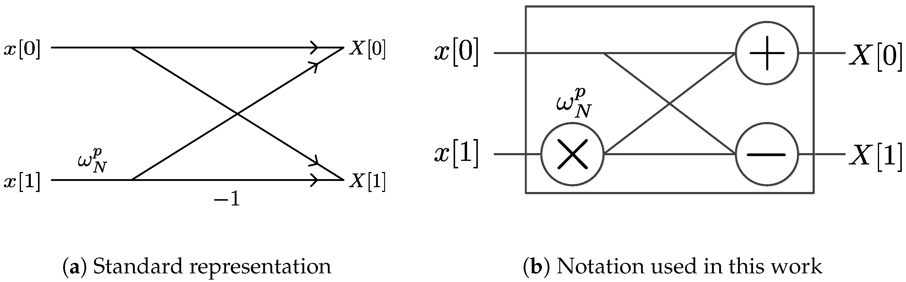
The Fast Fourier Transform (FFT) is the main block in many electronic communications, signal processing, and scientific computing operations. It allows for the fast computation of the Discrete Fourier Transform (DFT). The DFT, in turn, is used to obtain the spectrum of any finite discrete signal or numeric sequence. Many FFT factorizations have been proposed since its first formulation, including Cooley-Tucky, Pease, and Hartley, among others, each with different advantages and limitations [1]. As regularity becomes a desirable characteristic when FPGA-based solutions are pursued, this work uses the Pease FFT formulation due to its constant geometry structure [2,3]. Our work formulates a set of algorithms for addressing schemes or scheduling operations in FFT computations. Figure 1a shows the standard representation of a 2-point FFT calculation, also called a butterfly operation. In Figure 1b we introduce an alternate butterfly notation which we will use for the butterfly operation. This notation facilitates the formulation of FFT algorithms in terms of Kronecker products algebra, introduced later in this paper. An N-point FFT operation is divided into S stages, where is a positive integer.

Figure 1.
Representations for a 2-point Fast Fourier Transform (FFT) operation.
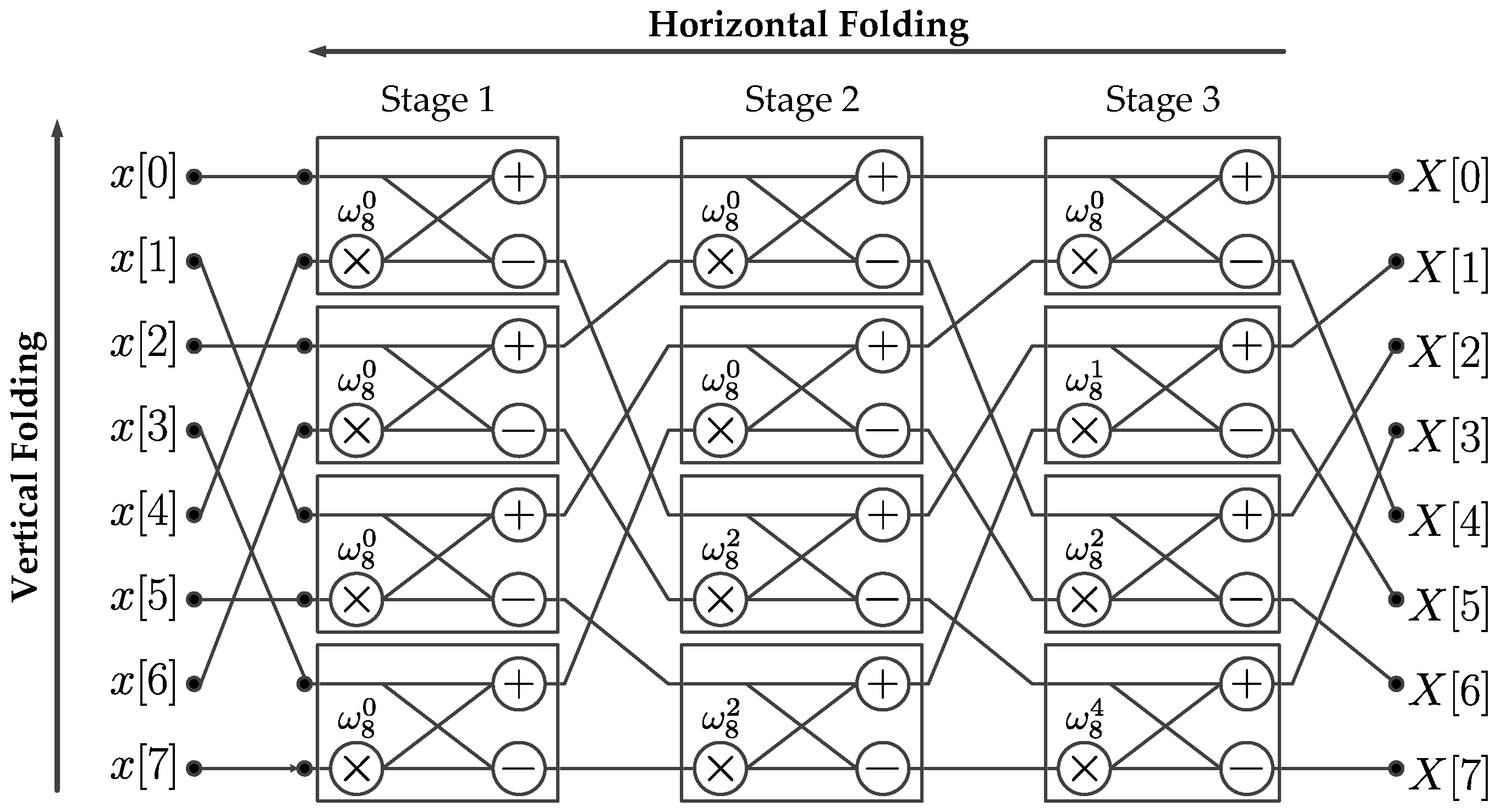
Figure 2 shows the structure of an 8-point Pease FFT implementation, illustrating a representative N-point structure where butterflies are presented as processing elements (PEs) in the rectangular boxes. Figure 2 also allows for introducing the concepts of horizontal and scalable vertical folding. A horizontal folding consists on reducing by half the number of columns in a FFT structure. A horizontal folding is considered maximum when successively halving the column count, reduces the total number of columns to one, maximizing the usability of hardware resources. The vertical folding consists on reducing the number of butterflies in the single column resulting resulting after a maximum horizontal folding has been applied. A vertical folding is considered scalable when the factor introduced to reduce the number of butterflies in the single column can be conveniently adjusted to fit a particular hardware resource limitation. A scalable vertical folding process affects the overall latency associated with memory operations. It also creates the need for a permutation block which is in charge of controlling the data flow between stages. A vertical folding factor is defined such that , where is defined as the number of memory banks required in the implementation, and is defined as the number of processing elements in a single column. A permutation block consists of two data switches and B memory banks. For small values of , the memory latency is high and the amount of consumed hardware resources is low. On the contrary, for large values of , the latency is low and the amount consumed hardware resources is high. The resulting structure may be classified as a Burst I/O design since the computation must wait for the entire FFT calculation to finish before providing a new input signal to the hardware computational structure (HCS).
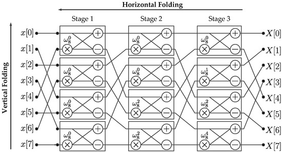
Figure 2.
8-point Pease FFT architecture.
Permutation blocks in folded hardware FFTs can be implemented in one of two ways: either using dedicated permutation logic or using address generation schemes. In the first approach, a complex dedicated logic circuit controls the data flow, while in the second, data are stored in memory banks and a simple controller generates the addresses depending on the needed permutations.
Several works have been reported using scalable permutation logic with variable number of points and folding factors. A major drawback of these approaches is the large amount of consumed hardware resources [4,5,6]. Addressing schemes were introduced by Johnson as an alternative able to significantly reduce the amount of consumed hardware resources [7]. Many FFT implementations have been reported to follow the concept of addressing schemes. Some have used a non-scalable approach targeted to specific applications [8,9,10,11,12]. Others provide scalable implementations in terms the number of FFT points [13,14,15,16,17,18,19,20,21].
Francheti et al. proposed a framework for the hardware generation of linear signal transforms [22]. Although their work produced functional solutions, this framework did not describe in sufficient detail the address generation scheme utilized in its table lookup procedure for twiddle factors or phase factors operations. It is essential to develop FFT computational algorithms with optimal data placement and access strategies, to obtain data accesses with zero conflicts. Data address generation schemes need to be designed to accomplish this task. Our address generation scheme satisfies this design requirement without the need of a reordering procedure, and it is independent of pipeline overlapping techniques, such as those reported in works by Richardson et al. [23].
Despite this diverse set of implementations, there are few approaches addressing the issue of using an HCS to allow for scalable folding processing. The main motivation behind this work is the existing need for a generalized addressing scheme for scalable algorithms based on maximum horizontal folding. To the best of our knowledge, no such generalized addressing scheme has been previously proposed. The key benefits of a our proposed addressing scheme can be summarized as follows:
- a set of methods to generate scalable FFT cores based on an address generation scheme for Field Programmable Gate Array (FPGA) implementation when the vertical folding factor is optimized,
- a mathematical procedure to automatically generate address patterns in FFT computations,
- a set of stride group permutations to guide data flow in hardware architectures, and
- a set of guidelines about space/time tradeoffs for FFT algorithm developers.
The rest of this paper is organized as follows: Section 2 describes the mathematical foundations of the FFT core. Section 3 describes the hardware implementation procedure. Section 4 evaluates the design performance in terms of clock latency and hardware resources when the target HCS is a Xilinx FPGA. Finally, Section 5 provides concluding remarks.
2. Mathematical Preliminaries
In this section, we start by presenting definitions and mathematical concepts used for the formulation of the proposed scalable address generation scheme.
2.1. Definitions
Let us first define two main matrix operations frequently used in this paper: Kronecker products and matrix direct sum. If and , then their Kronecker product is defined as [24], where
The matrix direct sum of matrix set is defined as
Now let us define the Pease formulation for an N-point FFT in Kronecker products,
where is a stride by 2 permutation of order N, is an identity matrix of size , is termed the bit reversal permutation of order N, and is the radix-2 butterfly defined as
is the twiddle or phase factor matrix defined as
where and,
where [25]. Furthermore, the direct computation shows that
where is, again, a stride by 2 permutation [26].
2.2. Kronecker Products Formulation of the Xilinx FFT Radix-2 Burst I/O Architecture
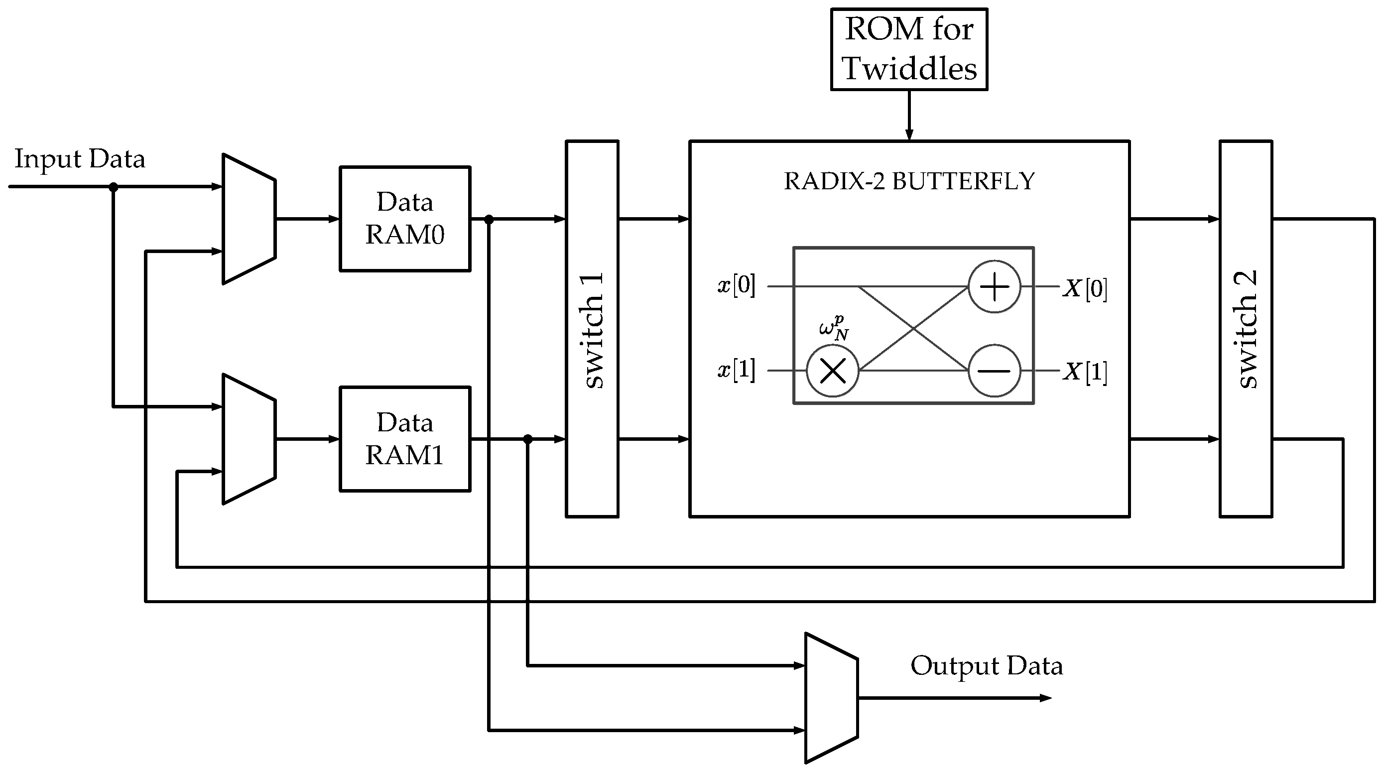
Our work is based on an equivalent architecture for the Xilinx FFT Radix-2 Burst I/O core (Figure 3) for implementing DFT computations [27]. Our goal is to present a systematic and scalable procedure for generating permutation-based address patterns for any power-of-2 transform size FFT algorithm and any folding factor. For this purpose, we propose to use the language of Kronecker products algebra as a mathematical tool. Therefore, we start by representing mathematically this architecture using a specific DFT computation example, for .

Figure 3.
Xilinx Radix-2 Burst I/O architecture. RAM: random access memory; ROM: read only memory
At the beginning of the process, in the Xilinx architecture, data points are stored serially in RAM0 and RAM1 through the input data bus (Figure 3). The first 4 data points are stored in RAM0 and the last 4 are stored in RAM1. Following the Pease FFT formulation, the addressing schemes can be expressed as:
where is the addressing scheme for RAM0, is the addressing scheme for RAM1, i is the stage identifier, and is a data exchange matrix. In the first stage, switch 1 in Figure 3 does not perform any permutation over the input data. In the rest of the stages, switch 1 does not perform any permutation in the first half, and interchanges the input data in the second half. That is,
where is the output of switch 1, is the input of switch 1, b is the internal step counter. The single butterfly operation can be expressed as:
where and are the radix-2 butterfly’s output and input in Figure 3, respectively. and,
where denotes the floor operation on a. Switch 2 in Figure 3 does not perform any permutation for the even-indexed values of b, the internal step counter. On the other hand, switch 2 interchanges the input data on the odd-values of b. That is,
where is the output of the switch 2 and is the input of the switch 2. This process applies for any value of N. The equations included in this subsection are presented as an example of how a signal transform hardware architecture can be represented mathematically under a unified computational framework.
It is important to notice that this architecture only uses one butterfly. What would happen with the addressing schemes, switches, and phase factor scheduling if two or more butterflies were used? the next subsection addresses this relevant issue.
2.3. Kronecker Products Formulation of the Scalable FFT with Address Generation
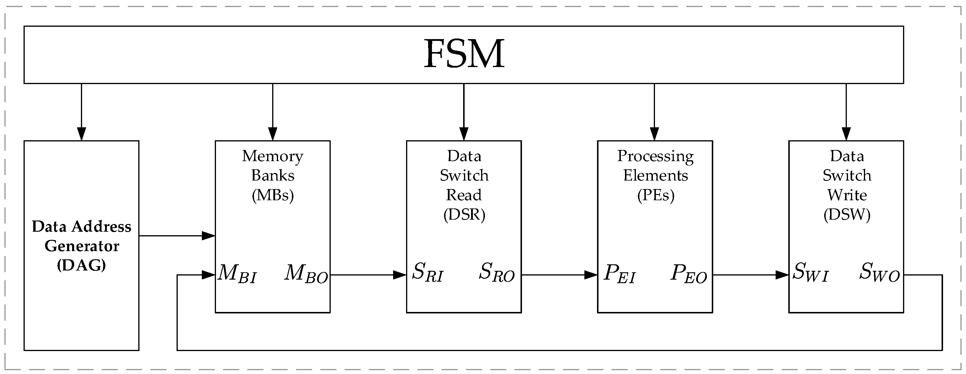
Figure 4 shows an FFT architecture designed with the required blocks for our addressing scheme, under the control of a Finite State Machine (FSM). The Data Address Generator (DAG) produces the addresses depending on the needed permutations. The Memory Banks (MBs) store the input signal and the processed data as well. The Data Switch Read (DSR) permutates the data points from the MBs to process them correctly. The Processing Elements (PEs) perform the mathematical operations. Finally, the Data Switch Write (DSW) permutates the data to avoid memory conflicts. Every block is mathematically represented as an entity, with specified inputs and outputs. To obtain these mathematical representations, we use again the language of matrix algebra and tensor or Kronecker products. In the next subsection, we define the general aspects of these mathematical representations.
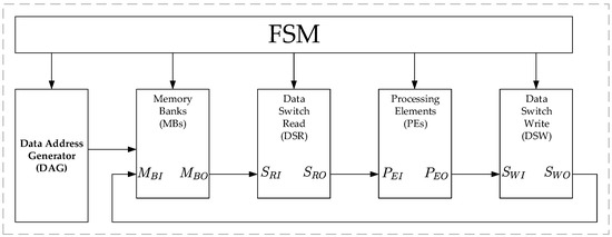
Figure 4.
FFT architecture with our proposed addressing scheme. FSM: Finite State Machine.
The DAG must perform two kinds of permutations over the data points, regardless of the folding factor: a bit-reversal permutation in the first stage and stride-2 permutations in the next stages. Furthermore, since our implementation is intended to be used as a “conflict free memory addressing strategy” [7], these permutations have to be performed by rewriting the data points into the same locations as being read. Since each butterfly needs two different values at the same time, different addressing schemes are needed. However, this work demonstrates that for any folding factor, only two array addressing schemes are needed. An array addressing scheme is defined as a systematic procedure for simultaneously pointing to B blocks of an ordered set of memory data. For an N-point FFT with vertical folding factor the array addressing schemes can be expressed as:
where is the even array addressing scheme, is the odd array addressing scheme, i is the stage identifier, is an exchange matrix, and are, again, a stride permutation and a bit-reversal permutation, respectively, and the superscript T denotes matrix transpose operation.
The addressing scheme requires B memory banks. Since each processing element or butterfly accepts two complex numeric values at the same time, and there are processing elements, the number of memory banks is equal to . Each memory bank consists of memory locations. The memory banks can be indexed using the following scheme,
where is the k-th memory bank, and is the internal step counter. We use row major storage which means that each row contains the complex numeric values of an entire memory bank. That is,
To extract the numeric values stored in the memory banks, we perform an inner product stage operation. This operation consists in first creating a state indexing matrix
and then performing the memory bank output () operation. We form this matrix by interleaving the even and odd array addressing schemes. That is,
where and are, again, the even and odd array schemes vectors respectively. Furthermore, we use the notation to refer the l-th element in k-th row in the i-th stage. Let be an ordered basis of column vectors with an entry of value one in the i-th position and zeros elsewhere. Let , termed a basis vector, denote the i-th element of order , of this basis, where i ranges from 0 to . That is,
The result of the inner product stage operation is the memory bank output (), and is obtained by making
where is the DSR input bus, is a basis vector, and
The numeric values fetched throughout these addressing schemes are the ones to be operated by the PEs at each stage, but they are not in the same order according to the butterflies arrangement.
The DSR permutates these numeric values. In the first stage, the DSR performs a bit reversal permutation over the input data. In the rest of the stages, the DSR performs stride-2 permutations in the first half of the stage, and modified stride-2 permutations in the second. That is,
where is the DSR output bus, and is the PEs input bus. The next action is to process the DSR output through the butterflies. The PEs are an arrangement of radix-2 butterflies represented as and is expressed as:
where is the DSW input bus, is a unit matrix defined as
and,
where and,
After the data points are processed by the butterflies, the results have to be stored in the same locations in the memory banks. However, to avoid memory bank conflicts, the results have to be permutated again. The DSW operator permutates these data points. For the even-indexed values of b, the internal step counter, the DSW does not perform any permutation. On the other hand, the DSW performs the next permutation on the odd-values of b. That is,
where is the DSW output bus, and is the input bus of the memory banks.
Let be an ordered set of row vectors with a zero in the i-th position and ones elsewhere. Let , termed a masking vector, denote the i-th element of order , of this set, where i ranges from 0 to . That is,
The next action is to write-back into the memory banks the numeric values contained in . This process can be done by making an addition. The operation is expressed as,
where the operator ⊙ denotes Hadarmard or entrywise product, the superscript T means matrix transpose operation and,
where is a masking vector. These formulations allow us to devise computational architectures associated with each expression. The next section describes how these expressions, called functional primitives, can be implemented as computational hardware architectures.
3. Hardware Implementation
3.1. Data Address Generator
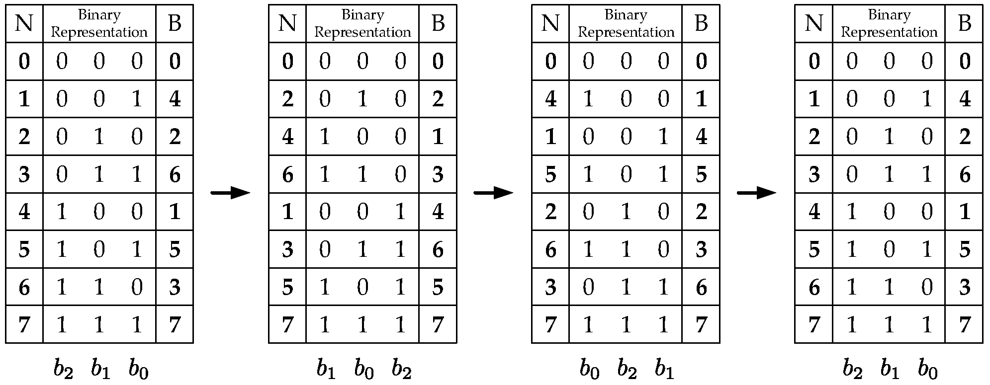
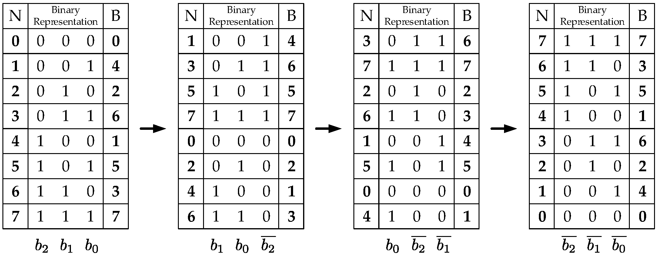
The hardware implementation of this block consists mainly of a standard-order counter and two blocks which modify the counter values. One block generates the addressing scheme for the even-indexed memory banks (Equations (16) and (17)). The other generates the addressing scheme for the odd-indexed memory banks (Equations (18) and (19)). The even-indexed memory banks require stride-2 permutations calculated throughout the stages making a left-circular shift over the previous addressing scheme. An example of how to generate the entire addressing scheme is shown in Figure 5. Similarly, the odd-indexed memory banks require modified stride-2 permutations which are calculated throughout the stages by making a left-circular shift and negating the least significant bit over the previous addressing scheme. Figure 6 shows an example of how to generate the entire addressing schemes Figure 5 and Figure 6 also show the decimal (N column) and decimal bit-reversal (R column) representations, respectively. Since it is easier to calculate the decimal representation, this is the one actually implemented. Nevertheless, the addressing scheme needed is the decimal bit-reversal representation. Therefore, all the address-generator outputs are bit-reversed to produce the correct addresses.
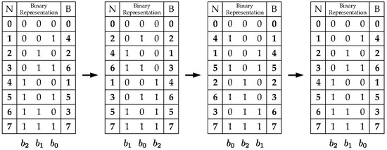
Figure 5.
Addressing scheme example for even-indexed memories ( and ).
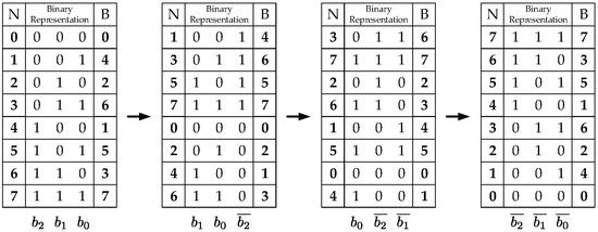
Figure 6.
Addressing scheme example for odd-indexed memories ( and ).
3.2. Phase Factor Scheduling
We took advantage of the periodicity and symmetry properties of the phase factors to reduce memory usage. Only numbers are stored, instead of as an FFT implementation normally requires [28]. The other values needed were obtained using,
Table 1 and Table 2 show the phase factor memory addresses. It is important to remark that the addressing scheme for the phase factors assumes memories of locations. Although we had established that the phase factor memories had locations. This is done due to the fact that the most significant bit of these addresses determines when Equation (36) is used. To establish an algorithm to generate the phase factors, we define three main parameters: the step (s), the frequency (f), and a parameter related with the initial value (n). The step s refers to the value to be added for obtaining the next address value, the frequency f refers to how often this step has to be added, and the initial value n is the first number in the addressing scheme. These main parameters behave as shown in Table 3. The frequency always starts at , decreases by halving its value in each iteration until the value is one, and remains as such until the calculation is over. The step always starts at , and also decreases by halving its value in each iteration until the value reaches the number of butterflies , and remains as such until the calculation is over. Finally, the parameter n, which represents the repetition and stride, at the same time, of the sequence of initial values, always stars at , decreases by making a right shifting operation until the value is zero. Algorithm 1 generates the twiddles address pattern for an implementation of size N and number of butterflies. In this Algorithm, T is the twiddle address, f is the frequency parameter, s is the step parameter, and n is the initial value.

Table 1.
Phase factor addressing scheme example ( and ).
Table 2.
Phase factor addressing scheme example ( and ).
Table 3.
Main parameters behaviour of the phase factor scheduling for .
Variable i represents the stage counter, b is the internal counter, and c is a counter. They are used to initialize the j-sequence per stage and to generate the addresses at each stage, respectively. Finally, R is a temporary variable used to store previous values of T.
| Algorithm 1: Twiddle Address. |
| Input: , , Output: Twiddle Pattern for N points and butterflies ; for to do ; for to do ; if is divisible by n and then ; end for to do if is divisible by f then ; end end end ; if then ; end if then ; end end |
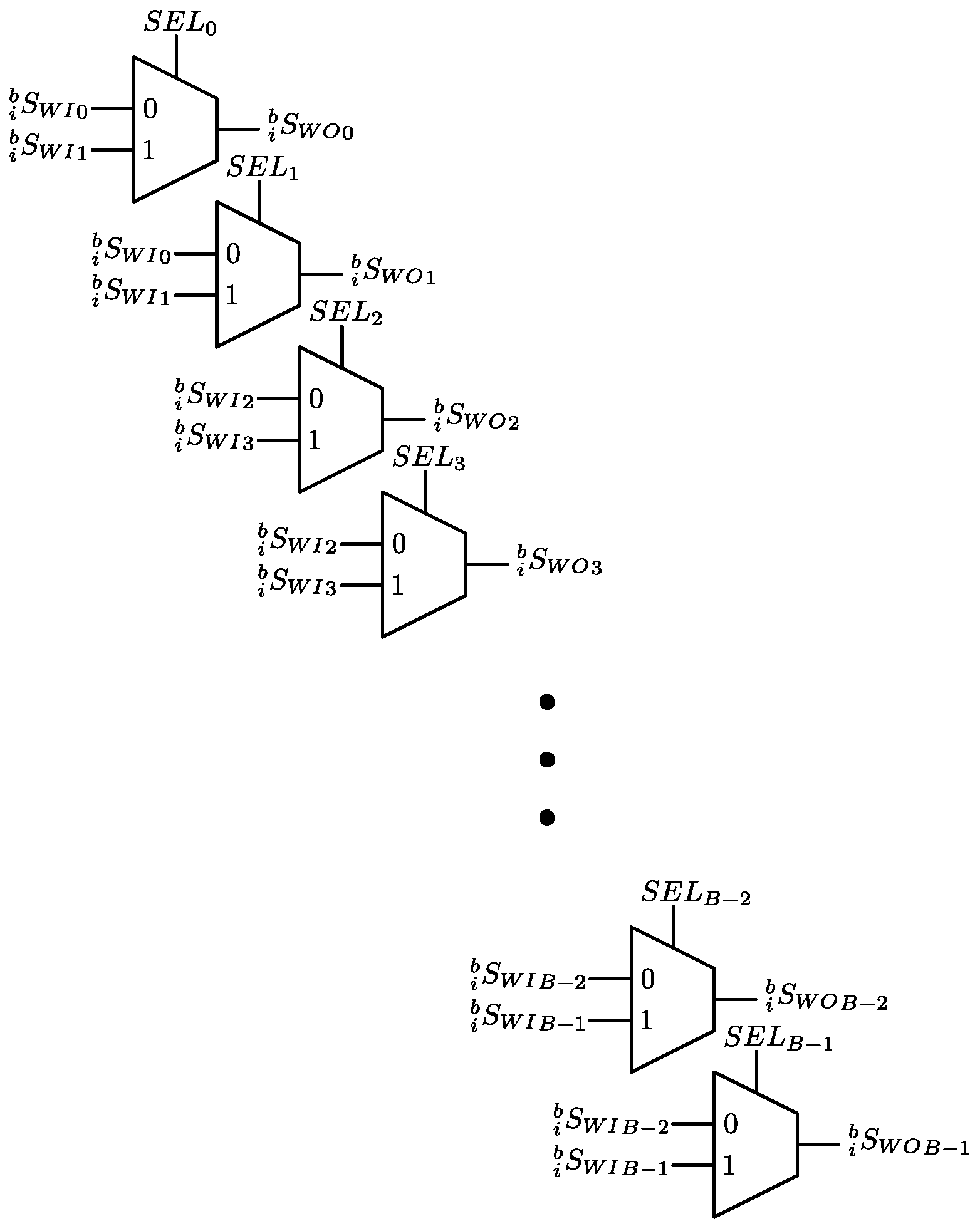
3.3. Data Switch Read (DSR)
In hardware, the Data Switch Read (DSR) is implemented as an array of multiplexers, as shown in Figure 7. To perform the permutations, every multiplexer must choose the correct input. Equation (27) shows these permutations. The bit-reversal, stride-2, and modified stride-2 permutations are generated with bitwise operations over a standard-ordered sequence, such as circular shifting and simple logical operations. A bit-reversal permutation is obtained by making the select input bus () equal to
where is, again, a bit-reversal permutation.
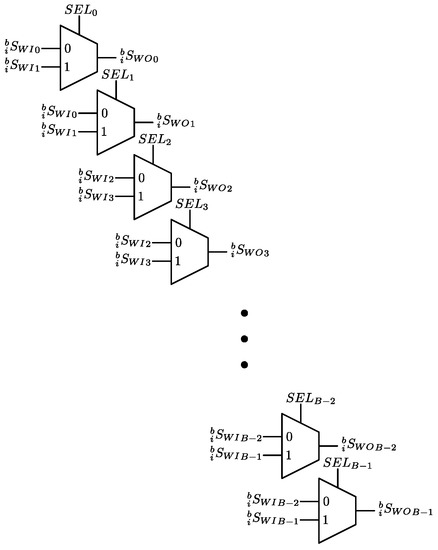
Figure 7.
Hardware Implementation of the DSR.
A stride-2 permutation is obtained by making the bus equals to
where is, again, a stride permutation. In hardware, this operation can be implemented by making a left circular shifting. A modified stride-2 permutation is also obtained by making the bus equal to
where and are, again, the exchange matrix and the identity matrix, respectively. In hardware, this operation can be implemented by making a left circular shifting only once, but negating the least significant bit.
3.4. Data Switch Write (DSW)
In hardware, the Data Switch Read (DSW) is also implemented as an array of multiplexers, as shown in Figure 8.
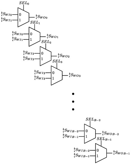
Figure 8.
Hardware implementation of the DSW.
Equation (32) shows the required permutations. The first permutation outputs the input data in the same order. That is,
The second permutation interchanges the even indexed input data with the next odd indexed input data. That is,
3.5. Finite State Machine (FSM)
The FSM is a simple two-state Mealy machine. In first state, the machine is in idle state, waiting for an enable signal. The second state performs the address calculation, returning to the first state when and . The FSM uses the values of i and b to successively generate the signals required to control:
- the output change of the DAG as indicated in Equations (17) and (19),
- the permutation to perform by the DSR and DSW as indicated in Equations (27) and (32),
- the phase factor addresses for the PEs and as indicated in Equation (28),
- the reading and writing process in the MBs as indicated in Equations (25) and (34).
4. FPGA Implementation
This section describes the procedure followed to validate the design. It shows the results obtained after completing the implementation of the proposed address generation scheme. The target hardware platform was a Xilinx VC-707 Evaluation Platform (Xilinx, Inc., San José, CA, United States). This particular board is based on a XC7VX485TFFG1761-2 FPGA (Xilinx, Inc., San José, CA, United States), which is a Virtex-7 family device. Resource consumption results were referenced for this specific chip. In order to provide a reference for comparison, a Xilinx FFT core v9.0 (Xilinx, Inc., San José, CA, United States) were included. Xilinx FFT IP core generator provides four architecture option: Pipelined Streaming I/O, Radix-4 Burst I/O, Radix-2 Burst I/O, and Radix-2 Lite Burst I/O. We concentrated on the Radix-2 architectures since they address the nature of our work. The Radix-2 Lite Burst I/O was not considered since is a simplified version of the Burst I/O version. Furthermore, the Pipelined Streaming I/O was not considered either since the architecture presented in this work optimizes the horizontal folding of any FFT computation.
It is important to emphasize that the Radix-2 Burst I/O architecture was designed to use a single butterfly performing simultaneously vertical and horizontal folding. Our architecture allows for a scalable vertical folding from butterflies (zero folding) to one butterfly (maximum folding). Hence, Radix-2 Burst I/O was chosen because it falls into the same category as the cores designed in this work. Our scalable vertical folding scheme may result in a time speed-up in a factor of .
4.1. Validation
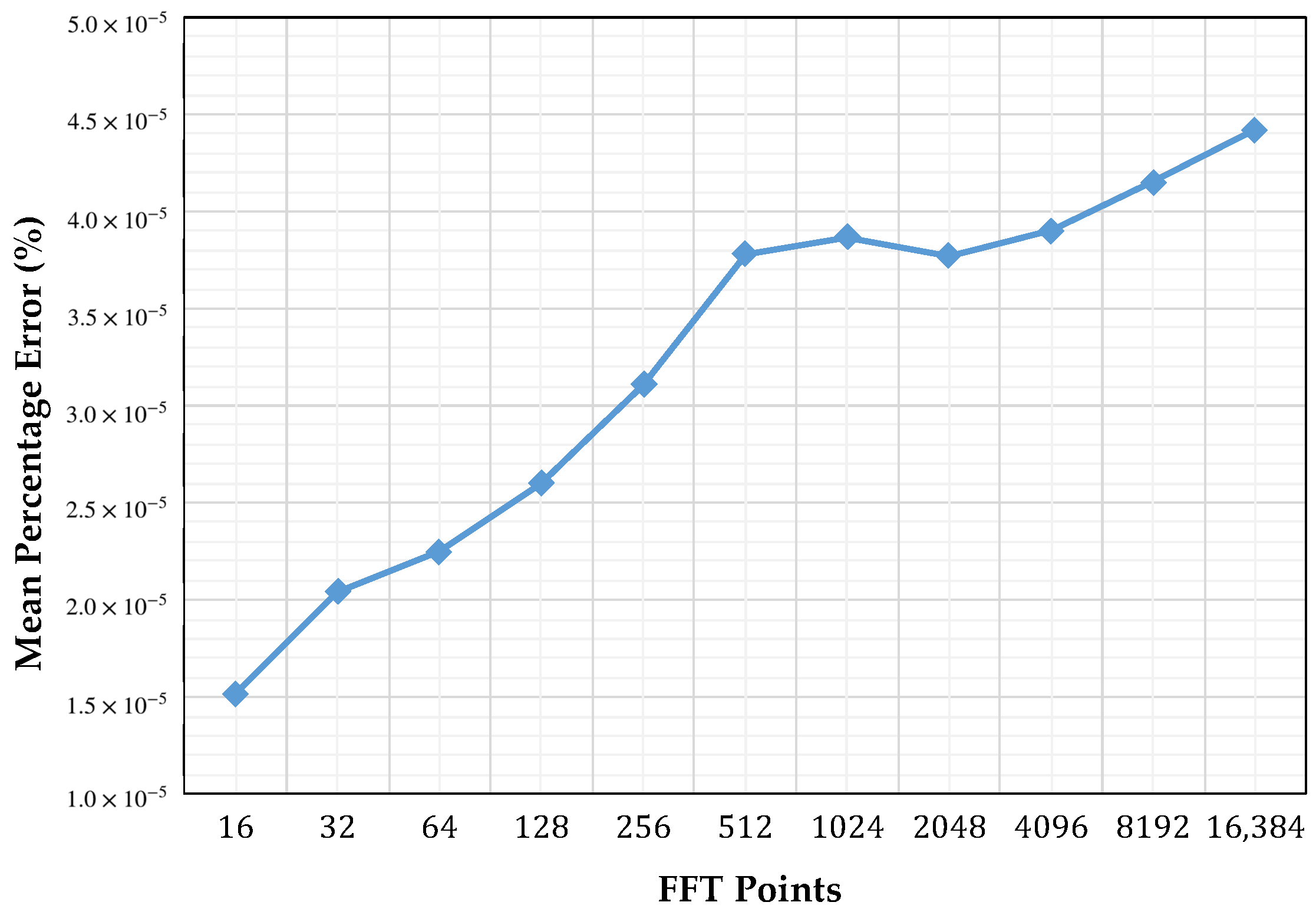
The implemented FFT with address generation scheme first went through a high level verification process. At this point, a MATLAB® program (MathWorks, Inc., Natick, MA, United States, 2014b) served to validate the correctness of the strategy by implementing the same dataflow that would be applied to the hardware version. After a hardware design was completed in VHSIC (very high speed integrated circuit) hardware description language VHDL, another program in MATLAB® was written with the purpose of generating random test data. These data were generated using the MATLAB® function rand, which generates uniformly distributed pseudorandom numbers. The data were then applied to the design by means of a text file. Then, the generated numbers were exported into MATLAB®, where they were converted into a suitable format for comparison with the reference FFT. After completing this procedure, we obtained the Mean Percent Error () of different implementations through the following formula:
where N is number of points, is data generated by MATLAB®, and is data generated by our FFT core in the target FPGA. This procedure was done for power of two transform sizes between and points, using one-, two-, and four-butterfly versions, and using single precision floating point format. Figure 9 illustrates of our core compared to the FFT calculated with MATLAB®. Figure 9 also shows that there is a minimum percent error of on an FFT core of 16 points and a maximum percent error of for an FFT core of 16,384 points. This information reflects an incrementing percent error while the number of points is increased. This is because MATLAB® uses double precision floating point format and rounding errors, which are produced by the large number of operations involved in the calculation. These results confirm that our scalable FFT core implemented using address generation scheme worked as expected.
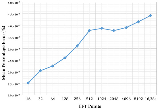
Figure 9.
Mean percentage error of our core with respect to MATLAB®’s FFT function.
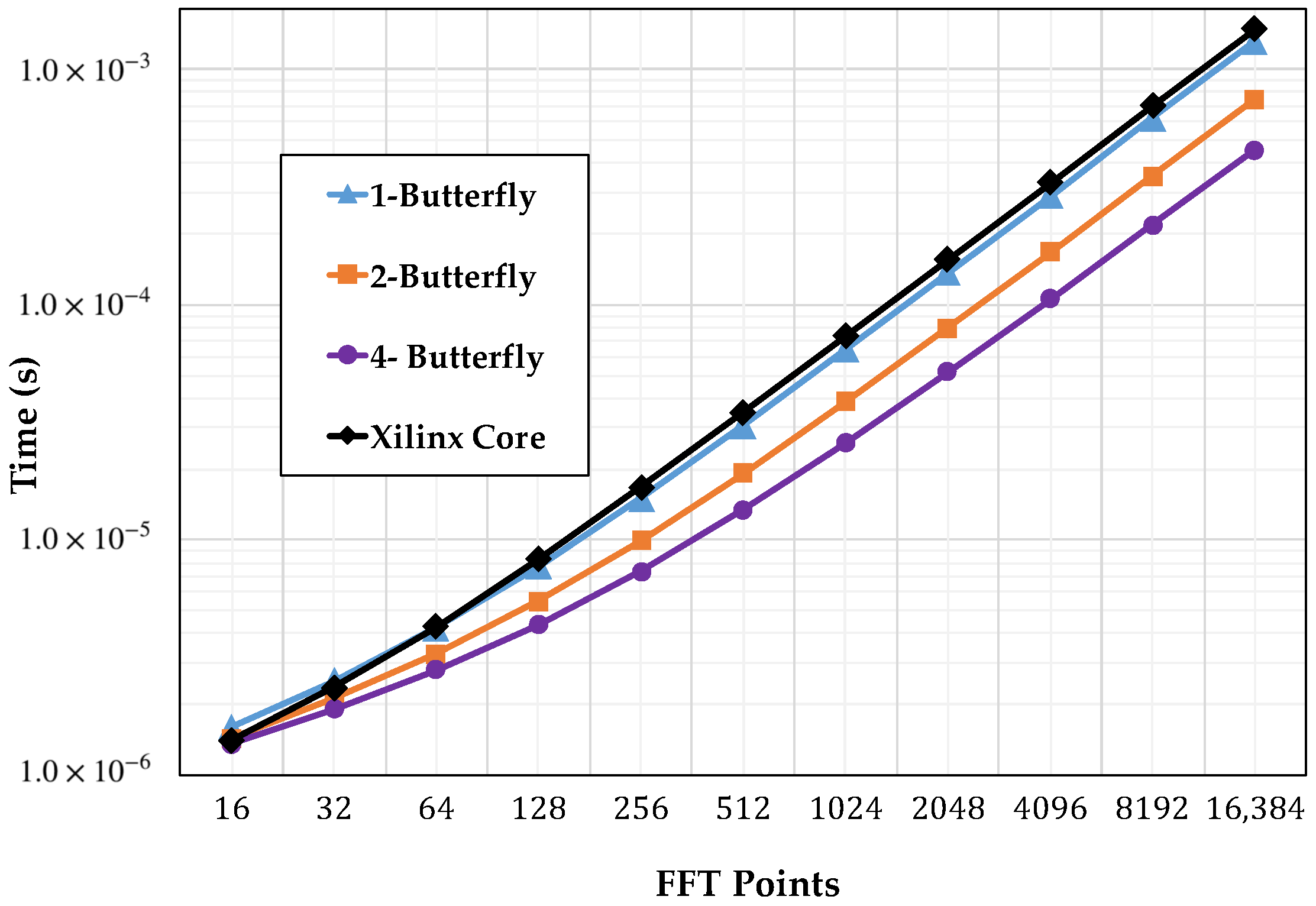
4.2. Timing Performance
In general, when applying the developed strategy, the number of clock cycles required to complete the operation is a well defined function of the transform size N and the number of butterflies used. This is, for a given transform of size N, with butterflies, and a butterfly latency , the cycles required to complete the calculation would be:
Figure 10 shows the computation times comparison of the core implemented with the one-, two-, and four-butterfly versions and the Xilinx version running at 100 MHz as a function of the number of points.
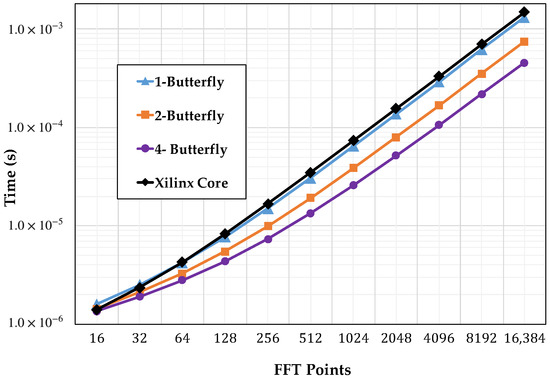
Figure 10.
Computation time.
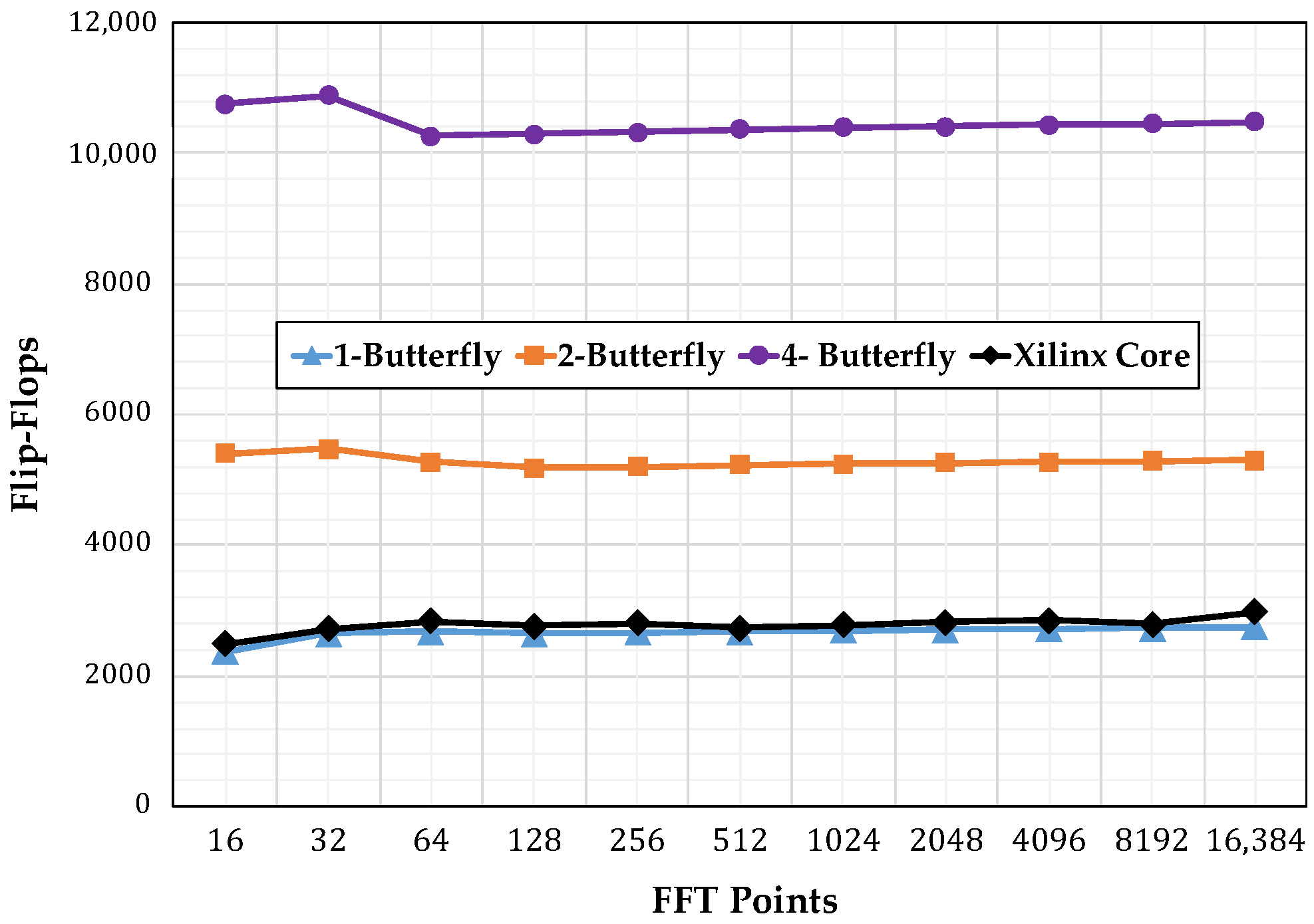
4.3. Resource Consumption
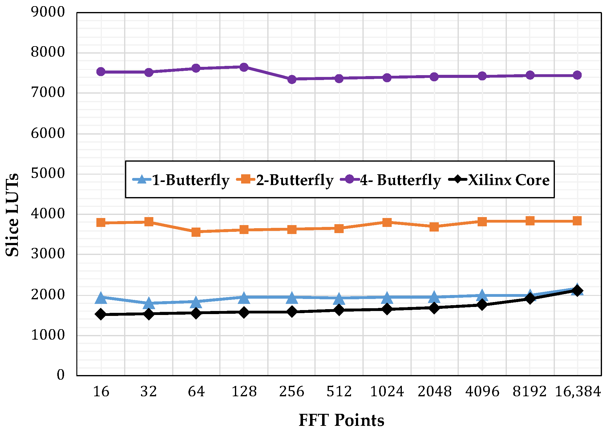
Figure 11 shows the number of slice registers consumed by the different implementations, starting with the single-butterfly to a four-butterfly version.Figure 12 shows the slice look up tables (LUTs) used. Finally, Figure 13 show the memory usage in terms of RAM blocks. The number of slices reflects the amount of logical resources spent. Flip-flops are contained within the slices and give information on how much resource is spent in sequential logic. The number of digital signal processing (DSP) blocks represents the amount of special arithmetic units from the FPGA dedicated to implement the butterfly. The total memory reflects the resources spent to store both, data points and phase factors. Regarding the DSP blocks consumed, each butterfly in this work uses 24 blocks, more than the used by the Xilinx Core. The XC7VX485TFFG1761-2 has 607,200 slice registers, 303,600 Slice LUTs, and 2800 DSP blocks.

Figure 11.
Flip-Flops consumption comparison.
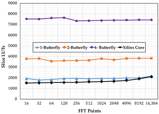
Figure 12.
Slice look up tables (LUTs) consumption comparison.
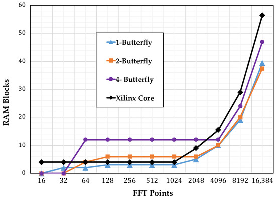
Figure 13.
Memory usage comparison.
4.4. Analysis
Figure 13 reveals that the most heavily affected resource was the memory, as its usage increased in proportion to the transform size. However, using our addressing scheme did not affect the consumption of memory resources. Figure 13 highlights this fact by showing that for increasing levels of parallelism the memory requirements were unaffected. Moreover, for a specific input size and phase factor, the data and address bus width increased proportionally to ; therefore, the system blocks managing these buses would not grow aggressively. The one-butterfly version had a smaller slice register consumption and almost the same slice count as the LUTs used by the FFT Xilinx Core. However, the two- and four-butterfly versions had a higher slice register and slice LUTs use. This was the trade-off to obtain a lower latency.
5. Conclusions
This paper proposed a method to generate scalable FFT cores based on an address generation scheme for FPGA implementation when the folding factor is scaled. The proposed method is an effective alternative to achieve a scalable folding of the Pease FFT structure. As a novel contribution, we provide a mathematical formulation to generate the address patterns and to describe data flow in FFT core computations.
Our approach is complete in the sense that it takes into consideration the address sequences required to access data points as well as twiddle or phase factors. This is accomplished by providing an algorithm and hardware to reproduce the twiddle factors for the Pease FFT radix-2 factorization regardless the number of points, folding factor, and numeric format using addressing schemes. Our implementation improves the computation time about with one butterfly, with two butterflies and with four butterflies when compared to a reference design of the FFT Xilinx Core.
Acknowledgments
This work was supported in part by Texas Instruments Inc. through the TI-UPRM Collaborative Program. The views expressed in this manuscript are the opinions of the authors and do not represent any official position of any institution partially supporting this research.
Author Contributions
Felipe Minotta conceived, designed, and performed the experiments; Manuel Jimenez contributed to analyze the data; Domingo Rodriguez contributed with the mathematical formulations. All authors contributed to the writing of the paper.
Conflicts of Interest
The authors declare no conflict of interest.
References
- Cooley, J.W.; Tukey, J. An Algorithm for the Machine Calculation of Complex Fourier Series. Math. Comput. 1965, 19, 297–301. [Google Scholar] [CrossRef]
- Pease, M.C. An Adaptation of the Fast Fourier Transform for Parallel Processing. J. ACM 1968, 15, 252–264. [Google Scholar] [CrossRef]
- Astola, J.; Akopian, D. Architecture-oriented regular algorithms for discrete sine and cosine transforms. IEEE Trans. Signal Process. 1999, 47, 1109–1124. [Google Scholar] [CrossRef]
- Chen, S.; Chen, J.; Wang, K.; Cao, W.; Wang, L. A Permutation Network for Configurable and Scalable FFT Processors. In Proceedings of the IEEE 9th International Conference on ASIC (ASICON), Xiamen, China, 25–28 October 2011; pp. 787–790. [Google Scholar]
- Montaño, V.; Jimenez, M. Design and Implementation of a Scalable Floating-point FFT IP Core for Xilinx FPGAs. In Proceedings of the 53rd IEEE International Midwest Symposium on Circuits and Systems (MWSCAS), Seattle, WA, USA, 1–4 August 2010; pp. 533–536. [Google Scholar]
- Yang, G.; Jung, Y. Scalable FFT Processor for MIMO-OFDM Based SDR Systems. In Proceedings of the 5th IEEE International Symposium on Wireless Pervasive Computing (ISWPC), Modena, Italy, 5–7 May 2010; pp. 517–521. [Google Scholar]
- Johnson, L.G. Conflict Free Memory Addressing for Dedicated FFT Hardware. IEEE Trans. Circuits Syst. II Analog Digit. Signal Process. 1992, 39, 312–316. [Google Scholar] [CrossRef]
- Wang, B.; Zhang, Q.; Ao, T.; Huang, M. Design of Pipelined FFT Processor Based on FPGA. In Proceedings of the Second International Conference on Computer Modeling and Simulation, ICCMS ’10, Hainan, China, 22–24 January 2010; Volume 4, pp. 432–435. [Google Scholar]
- Polychronakis, N.; Reisis, D.; Tsilis, E.; Zokas, I. Conflict free, parallel memory access for radix-2 FFT processors. In Proceedings of the 19th IEEE International Conference on Electronics, Circuits and Systems (ICECS), Seville, Spain, 9–12 December 2012; pp. 973–976. [Google Scholar]
- Huang, S.J.; Chen, S.G. A High-Throughput Radix-16 FFT Processor With Parallel and Normal Input/Output Ordering for IEEE 802.15.3c Systems. IEEE Trans. Circuits Syst. I Regul. Papers 2012, 59, 1752–1765. [Google Scholar] [CrossRef]
- Chen, J.; Hu, J.; Lee, S.; Sobelman, G.E. Hardware Efficient Mixed Radix-25/16/9 FFT for LTE Systems. IEEE Trans. Large Scale Integr. (VLSI) Syst. 2015, 23, 221–229. [Google Scholar] [CrossRef]
- Garrido, M.; Sanchez, M.A.; Lopez-Vallejo, M.L.; Grajal, J. A 4096-Point Radix-4 Memory-Based FFT Using DSP Slices. IEEE Trans. Large Scale Integr. (VLSI) Syst. 2017, 25, 375–379. [Google Scholar] [CrossRef]
- Xing, Q.J.; Ma, Z.G.; Xu, Y.K. A Novel Conflict-Free Parallel Memory Access Scheme for FFT Processors. IEEE Trans. Circuits Syst. II Express Briefs 2017, 64, 1347–1351. [Google Scholar] [CrossRef]
- Xia, K.F.; Wu, B.; Xiong, T.; Ye, T.C. A Memory-Based FFT Processor Design With Generalized Efficient Conflict-Free Address Schemes. IEEE Trans. Large Scale Integr. (VLSI) Syst. 2017, 25, 1919–1929. [Google Scholar] [CrossRef]
- Gautam, V.; Ray, K.; Haddow, P. Hardware efficient design of Variable Length FFT Processor. In Proceedings of the 2011 IEEE 14th International Symposium on Design and Diagnostics of Electronic Circuits Systems (DDECS), Cottbus, Germany, 13–15 April 2011; pp. 309–312. [Google Scholar]
- Tsai, P.Y.; Lin, C.Y. A Generalized Conflict-Free Memory Addressing Scheme for Continuous-Flow Parallel-Processing FFT Processors With Rescheduling. IEEE Trans. Large Scale Integr. (VLSI) Syst. 2011, 19, 2290–2302. [Google Scholar] [CrossRef]
- Xiao, X.; Oruklu, E.; Saniie, J. An Efficient FFT Engine With Reduced Addressing Logic. IEEE Trans. Circuits Syst. II Express Briefs 2008, 55, 1149–1153. [Google Scholar] [CrossRef]
- Shome, S.; Ahesh, A.; Gupta, D.; Vadali, S. Architectural Design of a Highly Programmable Radix-2 FFT Processor with Efficient Addressing Logic. In Proceedings of the International Conference on Devices, Circuits and Systems (ICDCS), Coimbatore, India, 15–16 March 2012; pp. 516–521. [Google Scholar]
- Ayinala, M.; Lao, Y.; Parhi, K. An In-Place FFT Architecture for Real-Valued Signals. IEEE Trans. Circuits Syst. II Express Briefs 2013, 60, 652–656. [Google Scholar] [CrossRef]
- Qian, Z.; Margala, M. A Novel Coefficient Address Generation Algorithm for Split-Radix FFT (Abstract Only). In Proceedings of the 2015 ACM/SIGDA International Symposium on Field-Programmable Gate Arrays, Monterey, California, USA, 22–24 February 2015; ACM: New York, NY, USA, 2015; p. 273. [Google Scholar]
- Yang, C.; Chen, H.; Liu, S.; Ma, S. A New Memory Address Transformation for Continuous-Flow FFT Processors with SIMD Extension. In Proceedings of the CCF National Conference on Compujter Engineering and Technology, Hefei, China, 18–20 October 2015; Xu, W., Xiao, L., Li, J., Zhang, C., Eds.; Springer: Berlin/Heidelberg, Germany, 2016; pp. 51–60. [Google Scholar]
- Milder, P.; Franchetti, F.; Hoe, J.C.; Püschel, M. Computer Generation of Hardware for Linear Digital Signal Processing Transforms. ACM Trans. Des. Autom. Electron. Syst. 2012, 17, 15. [Google Scholar] [CrossRef]
- Richardson, S.; Marković, D.; Danowitz, A.; Brunhaver, J.; Horowitz, M. Building Conflict-Free FFT Schedules. IEEE Trans. Circuits Syst. I Regul. Papers 2015, 62, 1146–1155. [Google Scholar] [CrossRef]
- Loan, C.F.V. The ubiquitous Kronecker product. J. Comput. Appl. Math. 2000, 123, 85–100. [Google Scholar] [CrossRef]
- Johnson, J.; Johnson, R.; Rodriguez, D.; Tolimieri, R. A Methodology for Designing, Modifying, and Implementing Fourier Transform Algorithms on Various Architectures. Circuits Syst. Signal Process 1990, 9, 450–500. [Google Scholar]
- Rodriguez, D.A. On Tensor Products Formulations of Additive Fast Fourier Transform Algorithms and Their Implementations. Ph.D. Thesis, City University of New York, New York, NY, USA, 1988. [Google Scholar]
- Xilinx, Inc. Available online: https://www.xilinx.com/support/documentation/ip_documentation/xfft/v9_0/pg109-xfft.pdf (accessed on 20 October 2017).
- Polo, A.; Jimenez, M.; Marquez, D.; Rodriguez, D. An Address Generator Approach to the Hardware Implementation of a Scalable Pease FFT Core. In Proceedings of the IEEE 55th International Midwest Symposium on Circuits and Systems (MWSCAS), Boise, ID, USA, 5–8 August 2012; pp. 832–835. [Google Scholar]
Sample Availability: Samples of the compounds ...... are available from the authors. |


© 2018 by the authors. Licensee MDPI, Basel, Switzerland. This article is an open access article distributed under the terms and conditions of the Creative Commons Attribution (CC BY) license (http://creativecommons.org/licenses/by/4.0/).