Abstract
In the present study, the effects of nitrogen incorporation on the transition of a p-type copper oxide semiconductor are investigated. The properties of sputtered copper oxide and nitrogen-incorporated copper oxide are evaluated and compared at various nitrogen gas flow rates. The results indicate that the addition of nitrogen results in an increased optical bandgap, accompanied by significantly reduced tail states compared to pristine copper oxide. In addition, X-ray diffraction and X-ray photoelectron spectroscopy reveal that the incorporation of nitrogen stimulates the transition from copper (II) oxide to copper (I) oxide.
1. Introduction
Recently, thin-film transistors (TFTs) based on metal oxide semiconductors such as In–Ga–Zn–O (IGZO) have attracted considerable attention for pixel-switching devices in flat-panel displays owing to their relatively high performance and stability compared to amorphous silicon (a-Si) [1,2,3]. Commercial products incorporating TFT backplanes based on n-type IGZO are already available in the market. On the other hand, relatively few reports are available on p-type oxide semiconductors.
Candidate p-type oxide semiconductors include copper oxide (CuOx), tin oxide (SnOx), and nickel oxide (NiOx) [3,4,5,6,7]. Among them, copper oxide is a non-toxic, cost-effective material that may be deposited by various techniques such as sputtering, chemical vapor deposition, and even the sol–gel method [8,9,10,11]. As a transition metal, copper oxide may exhibit two different phases, namely cupric oxide (copper (II) oxide, CuO) and cuprous oxide (copper (I) oxide, Cu2O). The monoclinic CuO and cubic Cu2O have optical bandgap energy values around 1.9–2.1 eV and 2.1–2.6 eV, respectively [12,13]. Generally, most amorphous oxide semiconductors have significantly low hole mobility compared to electron mobility, because of the localized valence band (VB) states resulting from highly directional O 2p orbitals. However, copper oxide exhibits a quite different orbital configuration of the VB states. The Cu 3d and O 2p orbitals are located at nearly the same energy level near the valence band maximum (VBM), and are fully occupied by hybridization. Such a configuration forms less-localized VBM states, creating relatively fast pathways for hole carriers [14,15,16]. Charge transport in copper oxide occurs mainly via charged Cu vacancies, which generate acceptor levels near 0.3 eV above the VBM [17,18]. To obtain high-performance, copper oxide-based p-type thin-film transistors, the former studies generally reported on the effect of annealing temperature, oxygen flow ratio during growth, and external dopant concentration [19,20,21,22]. Especially, the incorporation of nitrogen was observed to improve the electrical properties of copper oxide, yet the exact mechanism was not elucidated.
In the present work, the properties of CuO and N-incorporated CuO (CuON) thin films and the related TFTs are investigated. The results indicate that CuON has significantly decreased tail states compared to pristine CuO, as well as increased optical bandgap energy. Moreover, X-ray diffraction (XRD) and X-ray photoelectron spectroscopy (XPS) examinations reveal that the nitrogen incorporation in copper oxide stimulates the transition from copper (II) oxide to copper (I) oxide.
2. Experimental Section
CuxO and CuON thin films were deposited by reactive radio frequency (RF) magnetron sputtering at room temperature with a 3-inch diameter metal Cu target (99.99%). The applied RF power and gas mixing ratio of Ar/O2 were fixed at 80 W and 10:10 (sccm/sccm), respectively. The nitrogen gas flow rates were varied from 0 to 50 sccm. The working pressure values also varied from 7 to 22 mTorr as the amount of nitrogen gas was increased. The microstructures of CuxO and CuON thin films were analyzed by grazing incidence angle X-ray diffraction (GIAXRD) using a Cu kα radiation (D8 DISCOVER, Bruker AXS, Billerica, MA, USA). The surface morphologies were studied by atomic force microscopy (AFM). The chemical bonding states of nitrogen and oxygen components were examined by X-ray photoelectron spectroscopy (XPS) (K-ALPHA ESCA SYSTEM, ThermoFisher Scientificz, Waltham, MA, USA). The optical transmittance and bandgap values were extracted using a Transmittance UV-vis Spectrometer (S-3100, SCINCO, Seoul, Korea) in the range of 200 to 1000 nm. Hall measurements were also carried out to observe the electrical characteristics of thin films (HMS-5500, ECOPIA, Gyeonggi-do, Korea).
CuxO and CuON TFTs with bottom-gated structures were fabricated on highly doped p-type Si substrates with thermally grown 100-nm thick SiO2 gate dielectrics. After depositing the CuxO or CuON active layers, post-annealing was conducted at 300 °C for 2 h in a vacuum ambient by a rapid thermal annealing system (RTA). Then, the source–drain electrodes were formed using a shadow mask, by depositing a 100-nm thick nickel (Ni) film by thermal evaporation. The width and length of the resulting devices were 800 μm and 200 μm, respectively. The transfer characteristics were analyzed using an HP 4156B semiconductor parameter analyzer (HEWLETT PACKARD, CA, USA) in the dark under ambient conditions.
3. Results and Discussions
The XRD patterns of pristine CuxO exhibit intense (−111) and (111) peaks of a monoclinic structure at 2θ = 36 and 38°, respectively in Figure 1a. After annealing, the same peaks persist, as shown in Figure 1b. Similarly, the as-deposited CuON film also exhibits identical peaks; however, the (−111) peak is more intense compared to those of the as-deposited and annealed CuxO films (Figure 1c). On the other hand, the annealed CuON film exhibits a quite different structure. The corresponding diffractogram in Figure 1d exhibits the (111) and (200) peaks of Cu2O (N2 50 sccm). No apparent reaction between copper and nitrogen seems to have taken place, since even at relatively high nitrogen gas flow rates, no peaks related to compounds such as Cu3N are detected. At this point, it is suggested that nitrogen inhibits the oxidation of CuO and promotes the formation of the Cu2O phase. When nitrogen is incorporated in the plasma environment, nitrogen may play a role of removing oxygen gas as follows: 1/2O2 + N2 → N2O or O2 + N2 → 2NO. Figure 2 shows the AFM surface morphologies of CuxO and CuON layers. In the CuxO film, the root mean square (RMS) surface roughness is 0.83 nm, while CuON films grown with different nitrogen gas flow rates all exhibit relatively smooth surfaces with RMS roughness values no greater than 0.57 nm.
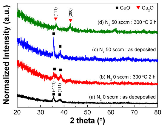
Figure 1.
XRD patterns of CuxO and CuON films. (a) as-deposited CuxO, (b) annealed CuxO, (c) as-deposited CuON, and (d) annealed CuON.
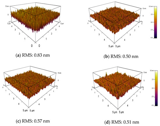
Figure 2.
Atomic force microscope images of films grown with (a) N2 0 sccm, (b) N2 10 sccm, (c) N2 20 sccm, and (d) N2 50 sccm.
The optical transmittance curves of CuxO and CuON layers were collected over a wavelength range of 200–1000 nm, as shown in Figure 3a. Figure 3b shows how Tauc’s law is used to extract the optical bandgap values of 1.99 and 2.49 eV for CuxO and CuON, respectively. After annealing, the optical bandgap values increased slightly up to 2.00 and 2.59 eV for CuxO and CuON, respectively. Therefore, the incorporation of nitrogen appears to affect the optical bandgap. Figure 3c shows the absorption coefficient spectra as a function of photon energy in the CuxO and CuON films. The tail state extending in the bandgap is called the Urbach tail, and its slope reflects the number of localized trap states. The small slope of the Urbach tail suggests that it has a large amount of localized trap state in the optical bandgap [20]. As the absorption spectra of pristine and annealed films in the subgap region show, CuON (i.e., the region of the green circle marked with Eg < 2.59 eV) layers exhibit smaller subgap defect absorption than CuxO (i.e., the region of the blue circle marked with Eg < 2.00 eV) films. At this point, it is highly likely that the presence of nitrogen results in decreased tail states.
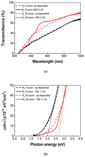
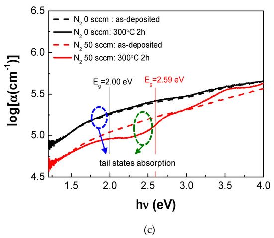
Figure 3.
(a) Transmittance spectra of as-deposited and post-annealed films grown under N2 0 and 50 sccm, respectively. (b) Optical bandgap with respect to N2 flow rates using Tauc’s plot. (c) The tail state absorption with respect to N2 flow rates.
XPS analyses were performed to observe the chemical bond properties in the films. The peak positions were calibrated using the C 1s peak, of which the standard binding energy is about 284.5 eV. Figure 4 shows the Cu 2p1/2 spectra of annealed CuxO and CuON. Both as-deposited CuxO and CuON thin films exhibit shoulder peaks around 954 eV and satellite peaks near 962 eV. Such satellite and shoulder peaks originate from copper (II) oxide [22,23,24]. The intensities of the satellite and shoulder peaks in CuON decrease largely after annealing, which strongly suggests that some transition from monoclinic CuO to cubic Cu2O has occurred. Such results are also in agreement with the XRD results shown in Figure 1. Figure 5a–d shows the O 1s peak spectra of the CuxO and CuON films. The peaks were resolved into two sub-peaks from metal oxygen bonds (M–O) and oxygen-related defects bond such as oxygen deficient sites (VO) and contamination species (OH-). Generally, it is well-known that the M–O, oxygen-related defects peaks in metal oxides are located near 530.6 eV and 531.9 eV, respectively [19,25,26]. In CuxO films, the O 1s sub-peak spectra did not change much after annealing, which suggests that no transition has taken place. However, the addition of nitrogen results in an increased oxygen-related defects peak portion from 20.9% to 34.9%, as is observed in pristine CuxO and CuON, respectively. It suggests that nitrogen incorporation may disturb Cu–O bonds and increase disordering or O-related defect density. However, as the CuON layers are annealed, the oxygen-related defects peak portion decreases considerably from 34.9% to 17.7%. While the migration of nitrogen forming Cu–N bonds may have contributed to the decrease in the intensity of the oxygen-related defects, the transition from CuO to Cu2O is also a probable factor. Figure 5e shows the N 1s peak of the pristine and annealed CuON thin films. The peak at 398.08 eV indicates the presence of Cu–N bonds [20]. In contrast, Cu–N bonds are not detected in pristine CuON, which implies that the incorporated nitrogen atoms are most likely to exist in the form of weakly bonded interstitials.
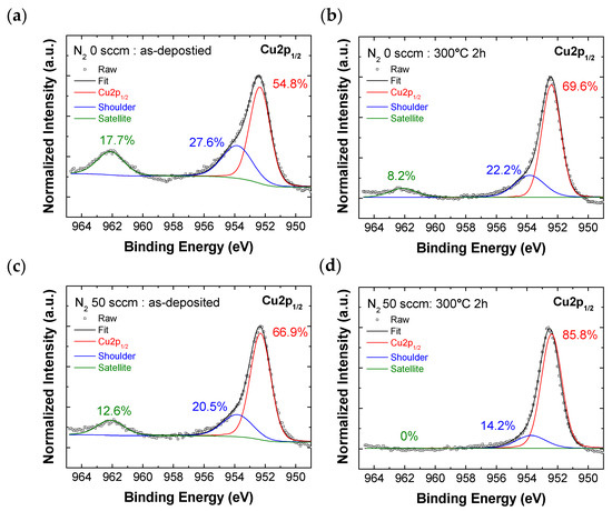
Figure 4.
X-ray photoelectron spectroscopy (XPS) Cu 2p1/2 peaks of (a) as-deposited CuxO, (b) annealed CuxO, (c) as-deposited CuON, and (d) annealed CuON.
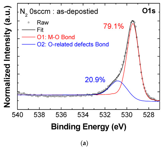
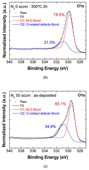
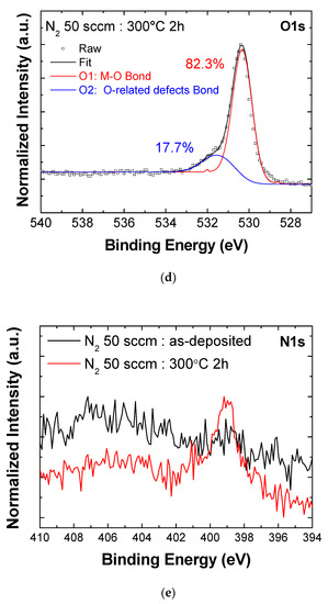
Figure 5.
XPS O 1s peaks of (a) as-deposited CuxO, (b) annealed CuxO, (c) as-deposited CuON, and (d) annealed CuON. (e) XPS N 1s spectra of as-deposited CuON and annealed CuON.
The relative atomic compositions of CuxO and CuON films are indicated in Table 1. Only the annealed CuON film exhibits a Cu:O composion ratio of 2:1, while the other samples exhibit Cu:O ratios near 1:1. In accordance with the XRD results, it may be concluded that the incorporated nitrogen promotes the transition from CuO to Cu2O after thermal treatment.

Table 1.
The atomic compositions of CuxO and CuON films obtained by XPS analysis.
Table 2 shows the Hall measurement results of CuxO and CuON thin films, which exhibited p-type behavior. As the nitrogen flow rate is increased during CuON growth, the carrier concentration values decrease from 2.24 × 10²⁰ to 3.59 × 10¹⁴/cm3, whereas the Hall mobility increases from 0.33 to 49.8 cm2/Vs. Generally, Cu2O exhibits relatively higher hole transport properties than CuO, even at relatively low carrier concentrations. Here, the increasing Hall mobility may be attributed to the presence of nitrogen, which helps to maintain the Cu2O phase.

Table 2.
Hall measurement results of CuON films grown at various N2 flow rates.
Figure 6a shows the transfer curves of CuxO and CuON TFTs with an optimized channel layer thickness at 10 nm. The gate-to-source voltage (VGS) is measured in the range of −30 to 30 V, and the drain-to-source voltage (VDS) is fixed at −30 V. The conductive characteristics of CuxO TFTs may be explained by the relatively high carrier concentration. The on–off current ratio and the field effect mobility of CuxO TFTs are 1.5 and 2.7 × 10⁻⁴ cm2/Vs, respectively. In contrast, the CuON TFTs show improved switching characteristics, with an on–off current ratio and field effect mobility of 7.4 and 6.93 × 10⁻³ cm2/Vs, respectively. It is highly anticipated that N 2p orbitals may further enhance the delocalization and hybridization of valence band states, which would enhance the p-type transport properties. CuxO and CuON TFTs have poor electrical properties due to the charge trap density between the active layer and the dielectric [19]. The output curve characteristics of the CuxO and CuON TFTs are shown in Figure 6b. While only linear properties are observed in the CuxO TFT, the CuON device exhibits clear pinch-off and current saturation without current crowding.
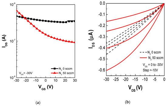
Figure 6.
(a) Characteristics of CuxO and thin-film transistors (TFTs) transfer curve according to N2 flow rates. (b) Output curves of the CuxO and CuON TFTs.
4. Conclusions
In the present work, the properties of CuO and CuON thin films and the related TFTs were investigated. Structural and chemical analyses indicate that the incorporation of nitrogen promotes the formation of the Cu2O phase. In the transmittance spectra, relatively small band tail states are observed in CuON compared to CuxO, indicating that CuON is less defective. Also, CuON films exhibit higher hole mobility than pristine CuxO. Such electrical characteristics are also reflected in the transfer and output curves of the corresponding TFT devices. The above results indicate that the nitrogen incorporation is an effective method not only to obtain a stable Cu2O structure, but also to enhance the p-type charge transport properties.
Author Contributions
S.-Y.A. performed the experimental work, analyzed data and wrote the paper; XPS measurement was performed by D.C.; K.P. assisted with XPS data analysis; J.P. and Y.J.K. assisted with writing and editing the paper; H.-S.K., supervised this work.
Funding
This work was supported by Basic Science Research Program through the National Research Foundation of Korea (NRF) funded by the Ministry of Education (Grant No: NRF-2019R1I1A2A01064153) and partially by the MOTIE (Ministry of Trade, Industry & Energy (Grant 10051403)) and KDRC (Korea Display Research Corporation) support program for the development of future devices technology for display industry.
Acknowledgments
The authors would like to thank Kim, H.D. and Jang, S.C. for supporting this study.
Conflicts of Interest
The authors declare no conflict of interest.
References
- Yang, D.G.; Kim, H.D.; Kim, J.H.; Park, G.; Kim, J.H.; Kim, Y.J.; Park, J.; Kim, H.S. Performance and stability of amorphous In-Ga-Zn-O thin film transistors involving gate insulators synthesized at low temperatures. J. Alloy. Compd. 2017, 729, 1195–1200. [Google Scholar] [CrossRef]
- Jang, S.C.; Park, J.; Kim, H.D.; Hong, H.; Chung, K.B.; Kim, Y.J.; Kim, H.S. Low temperature activation of amorphous In-Ga-Zn-O semiconductors using microwave and e-beam radiation, and the associated thin films transistor properties. AIP Adv. 2019, 9, 025204. [Google Scholar] [CrossRef]
- Yu, J.; Liu, G.; Liu, A.; Meng, Y.; Shin, B.; Shan, F. Solution-processed p-type copper oxide thin-film transistors fabricated by using one-step vacuum annealing technique. J. Mater. Chem. C 2015, 3, 9509–9513. [Google Scholar] [CrossRef]
- Matsuzaki, K.; Nomura, K.; Yanagi, H.; Kamiya, T.; Hirano, M.; Hosono, H. Epitaxial growth of high mobility Cu2O thin films and application to p-channel thin films transistor. Appl. Phys. Lett. 2008, 93, 202107. [Google Scholar] [CrossRef]
- Figueiredo, V.; Elangovan, E.; Barros, R.; Pinto, J.V.; Busani, T.; Martins, R.; Fortunato, E. p-type CuxO Films Deposited at Room Temperature for Thin-Film Transistors. J. Disp. Technol. 2012, 8, 41–47. [Google Scholar] [CrossRef]
- Sung, S.Y.; Kim, S.Y.; Jo, K.M.; Lee, J.H.; Kim, J.J.; Kim, S.G.; Chai, K.H.; Pearton, S.J.; Norton, D.P.; Heo, Y.W. Fabrication of p-channel thin-film transistors using CuO active layers deposited at low temperature. Appl. Phys. Lett. 2010, 97, 222109. [Google Scholar] [CrossRef]
- Sohn, J.; Song, S.H.; Nam, D.Y.; Cho, I.T.; Cho, E.S.; Lee, J.H.; Kwon, H.I. Semicond. Effects of vacuum annealing on the optical and electrical properties of p-type copper-oxide thin-film transistors. Sci. Technol. 2013, 28, 015005. [Google Scholar]
- Sanal, K.C.; Vikas, L.S.; Jayaraj, M.K. Room temperature deposited transparent p-channel CuO thin film transistors. Appl. Surf. Sci. 2014, 297, 153–157. [Google Scholar] [CrossRef]
- Barreca, D.; Comini, E.; Gasparotto, A.; Maccato, C.; Sada, C.; Sbervegloeri, G.; Tondello, E. Chemical vapor deposition of copper oxide films and entangled quasi-1D nanoarchitectures as innovative gas sensors. Sens. Actuator B Chem. 2009, 141, 270–275. [Google Scholar] [CrossRef]
- Jang, J.; Chung, S.; Kang, H.; Subramanian, V. P-type CuO and Cu2O transistors derived from a sol-gel copper (II) acetate monohydrate precursor. Thin Solid Films 2016, 600, 157–161. [Google Scholar] [CrossRef]
- Kim, S.Y.; Ahn, C.H.; Lee, J.H.; Kwon, Y.H.; Hwang, S.; Lee, J.Y.; Cho, H.Y. p-Channel Oxide Thin Film Transistors Using Solution-Processed Copper Oxide. ACS Appl. Mater. Interfaces 2013, 5, 2417–2421. [Google Scholar] [CrossRef]
- Zou, X.; Fang, G.F.; Yuan, L.; Li, M.; Guan, W.; Zhao, X. Top-Gate Low-Threshold Voltage p-Cu2O Thin-Film Transistor Grown on SiO2/Si Substrate Using a High-k HfON Gate Dielectric. IEEE Electron Device Lett. 2010, 31, 827–829. [Google Scholar]
- Refea, M.A.; Roushdy, N. Determination of the optical band gap for amorphous and nanocrystalline copper oxide thin films prepared by SILAR technique. J. Phys. D Appl. Phys. 2009, 42, 015413. [Google Scholar] [CrossRef]
- Han, S.; Flewitt, A.J. The origin of the High Off-State Current in p-Type Cu2O Thin Film Transistors. IEEE Electron Device Lett. 2017, 38, 1394–1397. [Google Scholar] [CrossRef]
- Fortunato, E.; Figueiredo, V.; Barquinha, P.; Elamurugu, E.; Barros, R.; Goncalves, G.; Park, S.H.; Hwang, C.S.; Martins, R. Thin-film transistors based on p-type Cu2O thin films produced at room temperature. Appl. Phys. Lett. 2010, 96, 239902. [Google Scholar] [CrossRef]
- Jun, T.; Kim, J.; Sasase, M.; Hosono, H. Material Design of p-Type Transparent Amorphous Semiconductor, Cu-Sn-I. Adv. Mater. 2018, 30, 1706573. [Google Scholar] [CrossRef] [PubMed]
- Han, S.; Niang, K.M.; Rughoobir, G.; Flewitt, A.J. Effects of post-deposition vacuum annealing on film characteristics of p-type Cu2O and its impact on thin film transistor characteristics. Appl. Phys. Lett. 2016, 109, 173502. [Google Scholar] [CrossRef]
- Nam, D.W.; Cho, I.T.; Lee, J.H.; Cho, E.S.; Sohn, J.; Song, S.H.; Kwon, K.I. Active layer thickness effects on the structural and electrical properties of p-type Cu2O thin-film transistors. J. Vac. Sci. Technol. B 2012, 30, 060605. [Google Scholar] [CrossRef]
- Yang, Y.; Yang, J.; Yin, W.; Huang, F.; Cui, A.; Zhang, D.; Li, W.; Hu, Z.; Chu, J. Annealing time modulated the film microstructures and electrical properties of P-type CuO field effect transistors. Appl. Surf. Sci. 2019, 481, 632–636. [Google Scholar] [CrossRef]
- Shijeesh, M.R.; Jayaraj, M.K. Low temperature fabrication of CuxO thin-film transistors and investigation on the origin of low field effect mobility. J. Appl. Phys. 2018, 123, 161538. [Google Scholar] [CrossRef]
- Nakano, Y.; Saeki, S.S.; Morikawa, T. Optical bandgap widening of p-type Cu2O films by nitrogen doping. Appl. Phys. Lett. 2009, 94, 022111. [Google Scholar] [CrossRef]
- Li, H.J.; Pu, C.Y.; Ma, C.Y.; Li, S.; Dong, W.J.; Bao, S.Y.; Zhang, Q.Y. Growth behavior and optical properties of N-doped Cu2O films. Thin Solid Films 2011, 520, 212–216. [Google Scholar] [CrossRef]
- Wang, Z.; Al-Jawhari, H.A.; Nayak, P.K.; Caraveo-Frescas, J.A.; Wei, N.; Hedhili, M.N.; Alshareef, H.N. Low Temperature Processed Complementary Metal Oxide Semiconductor (CMOS) Device by Oxidation Effect from Capping Layer. Sci. Rep. 2015, 5, 9617. [Google Scholar] [CrossRef] [PubMed]
- Akgul, F.A.; Akgul, G.; Yildirim, N.; Unalan, H.E.; Turan, R. Influence of thermal annealing on microstructural, morphological, optical properties and surface electronic structure of copper oxide thin films. Mater. Chem. Phys. 2014, 147, 987–995. [Google Scholar] [CrossRef]
- Jin, Z.; Liu, C.; Qi, K.; Cui, X. Photo-reduced Cu/CuO nanoclusters on TiO2, nanotube arrays as highly efficient and reusable catalyst. Sci. Rep. 2017, 7, 39695. [Google Scholar] [CrossRef]
- Zhnag, D.; Hu, B.; Guan, D.; Luo, Z. Essential roles of defects in pure graphene/Cu2O photocatalyst. Catal. Commun. 2016, 76, 7–12. [Google Scholar]
© 2019 by the authors. Licensee MDPI, Basel, Switzerland. This article is an open access article distributed under the terms and conditions of the Creative Commons Attribution (CC BY) license (http://creativecommons.org/licenses/by/4.0/).