1. Introduction
Nowadays, with the increasing demand for multi-standard, high data-rate wireless communications, voltage-controlled oscillators (VCOs) that are able to cover multiple frequency bands attract more and more attention. The capacitive tuned LC VCOs are preferred for their low phase noise and low power dissipation. An ultra-wideband VCO with a tuning range of 70% and a center frequency of 1.8GHz has been reported [
1]. For higher operation frequency or millimeter waveband, because the quality factor (Q) of the capacitor degrades rapidly with frequency, the tuning range is often kept relatively narrow for higher tank Q. To further increase the tuning range without sacrificing the tank Q, magnetic tuning has also been proposed, such as switched extra inductors that are coupled to the main inductors [
2,
3,
4], directly controlling the loop length of the main inductor in the LC tank [
5], switched guard-ring [
6], and switched substrate-shield [
7], that are artificial grounded metal shield to the inductor. In this way, better performance can be achieved for the tuning range, phase noise and power consumption. However, compared to conventional LC VCOs, the quality factor of the switchable inductor will significantly degenerate when the switch is at the ON-state due to the parasitic on-resistance [
8], resulting in poor phase noise and higher power consumption. Therefore, the magnetic tuning approach is not superior to conventional VCOs with discrete oscillating cores except for less area, unless the Q of the switchable inductor can be improved, especially at switch ON-state. Although a Q-boosted switched inductor has been implemented [
9], the work is related to PCB inductors with SMD PIN diode as RF switch for low-GHz applications. There are few works related to Q-boosting for on-chip switched inductors at ON-state or VCOs using Q-boosted switched inductor to improve phase noise at tens-GHz or millimeter-wave band.
In this article, the design of K-band low phase noise VCO based on Q-boosted switched inductor using NMOS transistor as the switch is presented. A quality factor boosting approach for the K-band on-chip switched inductor is proposed. The major design issues, such as the equivalent inductance, quality factor, and self-resonance frequency of the inductor at the switch ON/OFF states are analyzed and derived, based on the equivalent circuit. 1:n transformers with arbitrary parameter n are analyzed in the analytical expressions and design trade-offs are discussed, such as self-resonance frequency and Q limitation at the switch ON/OFF states. To avoid self-resonance frequency degeneration, a 1:2 transformer and an optimized switch size are utilized for the Q-boosted switched inductor. For comparison, both the proposed Q-boosted and the conventional switched inductors have been used for K-band VCOs design and fabrication in the 130 nm BiCMOS process. Measured results have shown an improved VCO phase noise at 100 kHz and 1 MHz offset by 2–5 dB at switch ON-state, with the proposed Q-boosted switched inductor.
2. Design and Implementation of the Low Phase Noise VCO with Q-boosted Switched Inductor
Figure 1 shows the schematic of the Colpitts VCO and equivalent circuits of the switched inductor at the switch ON and OFF states. The switched inductor consists of 1:n inductor-loaded transformer and NMOS transistor as the RF switch, which is connected to the secondary coil and controlled by Vsw. L
P and L
S are the self-inductances of the primary and secondary coil, k is the coupling coefficient, and n is the turn ratio. R
Soff, C
Soff, Y
Pon and C
Pon are the equivalent circuit parameters for the NMOS switch at the OFF/ON state. For simplification, the resistances and capacitances between the primary coil and secondary coil are omitted. Intuitively, for ideal conductive coil, the magnetically induced (eddy) current in the secondary coil is such that its resulting magnetic field will cancel the magnetic flux opposed by the excitation magnetic field of the primary coil. In order to cancel the same magnetic flux, the eddy current in the n-turn secondary coil will decrease to 1/n. Thus, the energy loss due to the switch on-resistance can be decreased to 1/n
2, leading to a boosted inductor Q.
In order to simplify the switch model, the ON-admittance Y
SW_ON = Y
Pon + jωC
Pon and OFF-impedance Z
SW_OFF = R
Soff + 1/(jωC
Soff) are simulated for the NMOS transistor with width of 6 µm, 10 µm, 14 µm, and channel length of 0.12 µm. The simulated results are shown in
Figure 2.
It is noted that, |Y
Pon| > 10 |jωC
Pon| and |1/(jωC
Soff)| > 5|R
Soff|, so C
Pon and R
Soff can be omitted for first-order simplification. The same simplified switch model can be found in [
2]. The excitation is applied to the primary coil (L
p), with voltage v
1 and current i
1,
The equivalent inductance L
eq and current in the secondary coil i
2 can be calculated with the following equations,
where k is the coupling coefficient and M is the mutual inductance between the primary and secondary coils. Then, at switch ON-state, the equivalent inductance L
eq_on and quality factor Q
Ind_on can be derived as.
At switch OFF-state, the self-resonance frequency ω
Res_off can be expressed as
From (6), if n
2ω(1 − k
2)L
pY
pon/k
2>>1/(n
2ωk
2L
pY
pon), the former term will be the main contributor to Q
Ind_on, which will linearly increase as n
2 increases. To achieve this,
is equally required. For typical ω of ~2π·25 GHz, L
p of ~500 pH, and k of ~0.5, n
2Y
Pon should be much larger than 14.7 mS, which means the inductor Q will increase at the ON-state if using the larger size for the switch transistor, or more turns for the secondary coil. However, this will also lead to large parasitic capacitance at the switch OFF-state, and degeneration of inductor operation frequency because the self-resonance frequency will decrease with 1/n
2, as derived in (7). To demonstrate the Q-boosting effect at K-band, W = 10 µm and n = 2 are chosen in the following design.
Figure 3a,b shows the normal switched inductor with a secondary turn of n = 1 and the proposed Q-boosted switched inductor with n = 2. Top metal layer with a thickness of 4 µm and height to the ground of 9.62 µm has been used for the inductor for high Q application. The design is co-simulated with Agilent Advanced Design System (ADS) and Ansoft High Frequency Structure Simulator (HFSS).
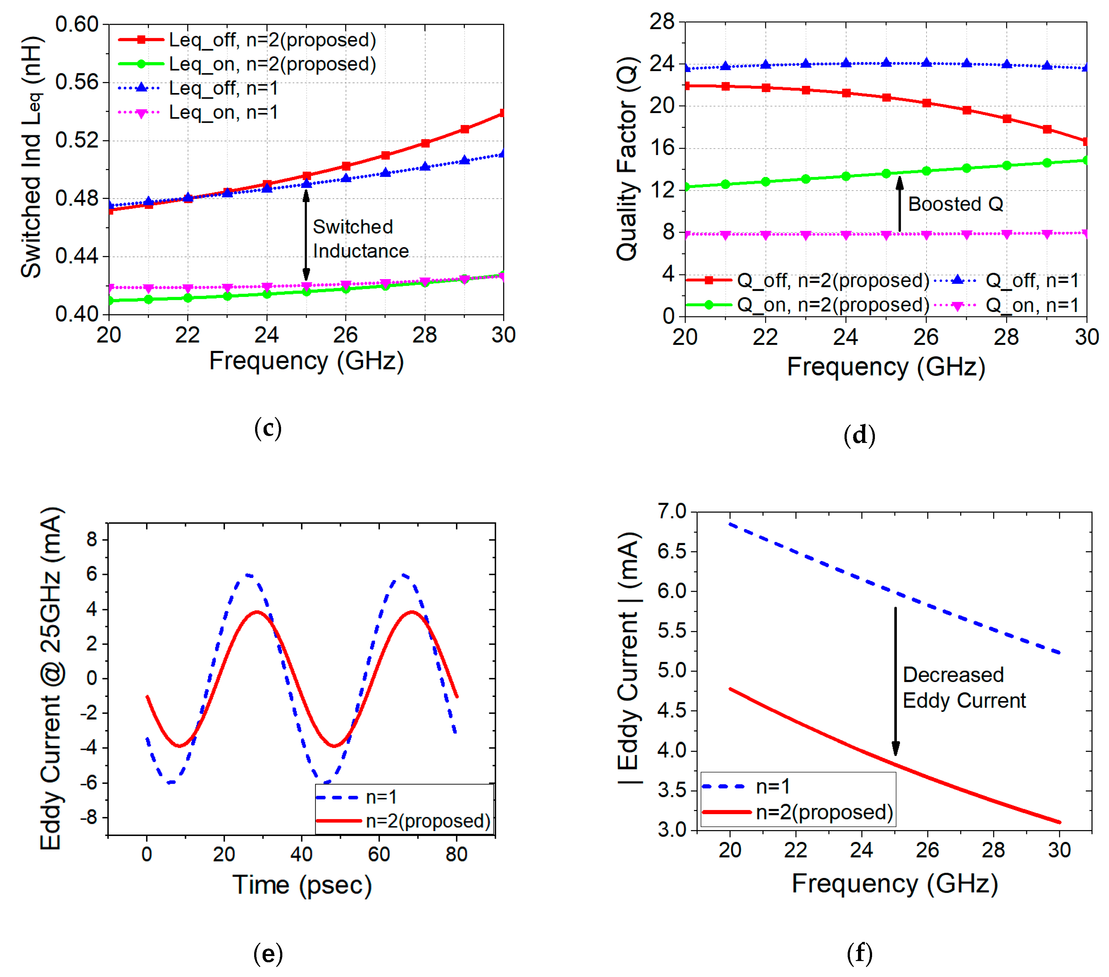
Figure 3c shows the simulated inductance L
eq. At 25 GHz, the L
eq can be reconfigured as 0.42 nH/0.49 nH (ON/OFF-state) for the normal switched inductor (dashed line), and 0.416 nH/ 0.496 nH (ON/OFF-state) for the proposed Q-boosted switched inductor (solid line).
Figure 3d shows the simulated quality factor Q. At the ON-state, the Q-boosted switched inductor has Q of 12.3–14.8 for 20–30 GHz, while the normal switched inductor has Q of 7.8–8. This shows that the quality factor can be improved with the proposed Q-boosting technique. It is noted because the derivation of (1)–(4) does not take into account the resistance of the secondary coil and other ohm-loss in the inductor, the Q-boosting factor is much less than n
2. At the OFF-state, this technique will degenerate the Q from 23.8 to 16.6–21.9, which results from larger parasitic capacitance and resistance of the secondary coil at OFF-state. But this degeneration is acceptable, because the overall Q of the switched inductor is mostly limited by the ON-state performance. To further validate the proposed Q-boosted approach, 1 V peak-peak differential AC-voltage-source has been used as input at the primary inductor, and the Eddy currents on the NMOS transistor and secondary inductor are simulated at the switch ON-state.
Figure 3e shows the transient Eddy currents at 25 GHz with the normal switched inductor (dashed line) and the proposed Q-boosted switched inductor (solid line). The amplitude of the sinusoid Eddy current for n = 2(proposed) is 3.8 mA, while the Eddy current for n = 1(conv) is 6.0 mA.
Figure 3f shows the magnitude of the Eddy currents from 20–30 GHz, which is 1.5–1.6 times higher on conventional inductor than that on the proposed inductor. With the same NMOS transistor RF switch, smaller eddy current means smaller ohm-loss for the same ON-resistance, thus boosted inductor Q. Then, K-band Colpitts VCOs are designed with the Q-boosted switched inductor and normal switched inductor, for comparison. As shown in
Figure 1, the LC tank consists of C
1, C
2, L
2, C
var, L
e, and the switched inductor L
eq. C
var is the capacitance of the varactor, which is biased with tuning voltage, V
t. Bipolar transistor T
1 generates the desired negative resistance to sustain oscillation. The biasing condition for T
1 and T
2 are optimized for noise and output power. The emitter lengths for T
1 and T
2 are 18 µm and 10 µm, respectively. Differential outputs
f0+ and
f0− are combined with balun for single-end output. Finally, the designed Colpitts VCOs are fabricated with 130 nm BiCMOS process, which is shown in
Figure 4, with a core size of 860 µm × 690 µm, excluding the pads.
3. Results
The K-band Colpitts VCO chips are wire-bonded to the PCB board for DC biasing and tested with Zprobe GSG probe. The output spectrum and phase noise of the VCOs are measured with R&S signal source analyzer FSUP50, which also provides biasing voltage V
dd, V
b V
t, V
sw to the chip.
Figure 5a shows the measurement setup environment, and
Figure 5b shows the output spectrum for the Colpitts VCO with the Q-boosted inductor, where the VCO outputs 3.7 dBm (after calibration) at 25.557 GHz, with V
dd = 2.8 V, I
dd = 35 mA, at V
t = 0.3 V, and V
sw = 0 V.
Figure 6a shows the output frequency range of VCO with Q-boosted switched inductor is from 24.998 to 27.134 GHz for switch OFF-state (V
sw = 0 V), and 26.432 to 28.672 GHz for switch ON-state (V
sw = 1.2 V), which is very close to the frequency tuning range of VCO using conventional switched inductor.
Figure 6b shows the measured VCO phase noise from 100 kHz to 10 MHz offset under the switch ON/OFF states, when V
t = 0.8 V. VCO using the conventional inductor shows best phase noise at the switch OFF-state (V
SW = 0 V) (red solid line), with −91dBc/Hz@100 kHz, and −112.1dBc/Hz@1MHz. However, the phase noise at switch ON-state (V
SW = 1.2 V) (black dot line) degenerates by ~7 dB to −84dBc/Hz@100kHz, and −105.2dBc/Hz@1MHz. This is expected because of the decreased inductor Q at the switch ON-state, as shown in
Figure 3d. For the VCO using proposed Q-boosted inductor, the phase noise at switch OFF-state (purple dash line) is −89.1dBc/Hz@100kHz and −110.7dBc/Hz@1MHz. At switch ON-state (blue dash-dot line), the phase noise gently decreases to −87.4dBc/Hz @100kHz and −109.6dBc/Hz@1MHz. The proposed Q-boosting technique successfully improves VCO phase noise at the switch ON-state by 3.4–4.4 dB for 100 kHz and 1 MHz offset. The phase noise improvement at 10 MHz offset is less than ~1.5 dB at the switch ON-state, because it’s close to the phase noise floor, which is mainly dependent on the active device and the output power level of oscillators [
10]. This can also be further explained with the following phase noise equation,
where
L{Δω} is the phase noise at the frequency offset Δω from the carrier frequency ω
0,
F is the phase noise figure from the active device,
PSig is the output power of the oscillator,
Q is the quality factor of the LC tank, Δω
1/f3 is the 1/f
3 corner frequency. At extremely small frequency offsets, the phase noise is mainly contributed by the flicker noise from the active device, which is dependent on the device itself, and difficult to suppress by tank Q. For frequency offset between Δω
1/f3 and ω
0/2Q, the phase noise is mainly contributed by the up-converted thermal noise, which can be filtered by the RLC tank, so increased Q can help to suppress the phase noise in this region. At large frequency offset, the phase noise is basically the fixed thermal noise floor, which can be improved with increasing output signal power.
It is noted that the Q-boosting technique will slightly degenerate phase noise at switch OFF-state by ~1dB, due to larger parasitic capacitance and resistance of the secondary coil. This is acceptable because the overall phase noise is mainly limited by ON-state performance, as shown in
Figure 6b. Phase noise comparisons across full tuning range at switch ON state is shown in
Figure 6c. It is clear that the proposed Q-boosting technique has typically improved the VCO phase noise at switch ON-state by 2–5dB for 100 kHz and 1 MHz offset. Comparison of reported VCOs using switched inductor is listed in
Table 1.


