1. Introduction
The demand for services in current communications networks has experienced a heavy growth in recent years, and it is predictable that this trend will continue in the future, or even rise, because consumers demand access to an increasing amount of information using more and more different devices [
1]. From the standpoint of service providers, this poses a severe challenge in terms of research and innovation in the design and implementation of communications systems.
DVB-T tuners have been reported for some years, with realizations in the early 1990s [
2], and have since remained a popular field of research [
3,
4,
5,
6,
7,
8]. They have a wide spread both in the technology in which they are implemented, which ranges from standard Si CMOS technologies of down to 40
[
7] to other technologies such as SiGe BiCMOS [
6]. Also, they are typically intended for direct RF antenna inputs in the available bands (UHF, VHF, L-band...).
One field of active research in the communications industry is broadband global networks, which today allow providers to offer jointly high-speed access to the Internet, telephone lines and television broadcasting using a single network to the end user. The concept of combining these three services is referred to as
triple-play. The first attempt to deploy triple-play commercially was carried out in Italy back in 2001 by the operator Fastweb, using a fiber-to-the-home (FTTH) infrastructure [
9]. This strategy was proven right and allowed them to lead in the average revenue per user (ARPU) rankings for some consecutive years [
10], which has fueled most telecommunications operators to follow this approach. Presently, FTTH networks are being deployed to offer triple-play solutions around the world.
To provide triple-play, operators must have a network capable of carrying all three services simultaneously. Of them, the most demanding one in terms of bandwidth is television broadcasting, which today typically requires 10 Mbit/
–15 Mbit/
alone [
11]. With today’s technology, network infrastructures suitable for triple-play services can be deployed based on copper, cable or optical fiber, although the latter shows a clear advantage in terms of bandwidth [
12]. Besides this, networks based on optical fiber also introduce lower attenuation, which allows covering larger distances between provider and clients; they permit the implementation of point-to-multipoint (P2MP) tree structures; and, consisting of passive elements, they are very cost-efficient and easy to maintain. For this reason, networks based on passive optical fiber with gigabit capabilities (GPON) are the preferred choice to implement FTTH for triple-play solutions [
1].
In a conventional triple-play implementation, both telephone lines and television broadcasts tend to be IP services (VoIP and IPTV, respectively) that along with Internet access, share the whole bandwidth of the subscriber. Typically, telephone lines and Internet provision share a common background among service providers, but the broadcast of television contents in triple-play brings with it a series of issues that need to be addressed separately. Among them, the most critical one is the saturation of the clients’ available bandwidth, which is even more pressing with the demand of contents featuring ultra-high definition (UHD) at 4K or even 8K.
In this respect, practical implementations to deliver 4K and 8K contents require, respectively, over 20 Mbit/
and 40 Mbit/
of bandwidth, if virtual reality (VR) content needs to be streamed, even with compression [
13]. This bandwidth needs to be taken from the clients’ overall bandwidth, thus limiting the capabilities for other services, which in turn require an increasing bandwidth to allow the simultaneous use of several different devices at home. This issue is even more critical if we take into account that in a typical household, several television sets might be used at the same time to watch different channels, each of them requiring its own bandwidth.
2. Broadcast Architecture
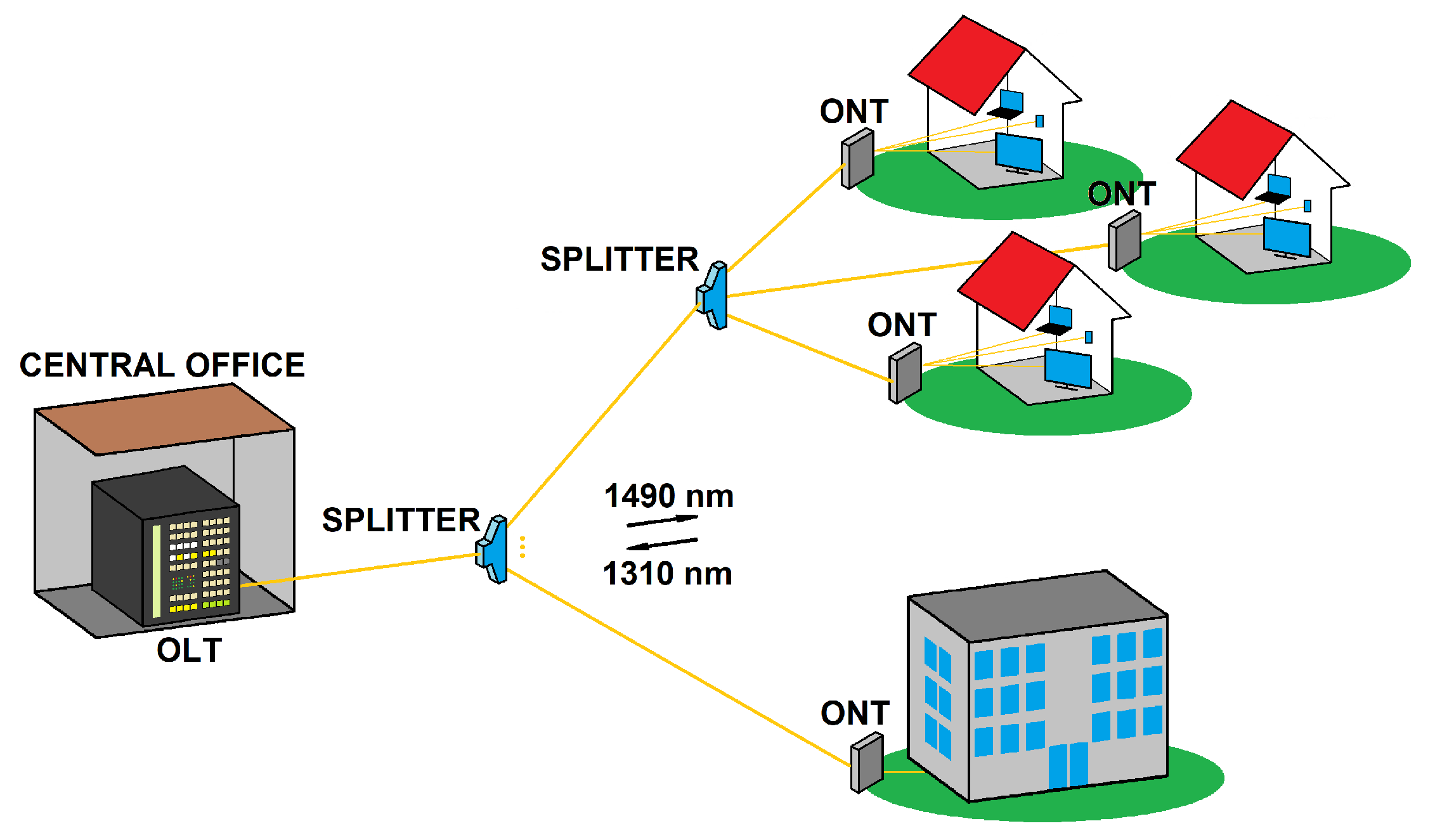
GPONs have a tree P2MP structure with passive optical splitters (typically 1:32 or 1:64) to divide the signals and drive them from the service provider endpoint, called
optical line termination (OLT), to the customer premises, where a piece of equipment called
optical network terminal (ONT) allows the obtaining of the services (Internet, television and telephone) provided with triple-play. Both the up- and down-links in a GPON use the same optical fiber, which is shared using wavelength division multiplexing (WDM).
Figure 1 shows a scheme of the distribution of contents in a GPON network from the OLT to the different ONTs, both in residential and industrial areas.
A standard implementation of GPON uses
class-B transceivers, which allow a transmitter laser power of over 1 dBm and a receiver sensitivity of
dBm [
14]. Because one splitting stage introduces roughly 20 dB of attenuation, and the typical losses of the fiber are
dB/
, the above figures mandate that the distance between the OLT and the ONT in a GPON cannot be longer than 20
[
14].
In terms of the transmitted signal, as it is shown in
Figure 1, the down-link uses only one carrier at a wavelength of 1490
, which is modulated directly at the OLT at a maximum speed of
Gbit/
. This signal is then broadcast to all the users connected to the GPON, and it is every ONT that filters out the traffic that is not directed to it. The up-link, in turn, uses time-division multiplexing access (TDMA) to avoid collisions with the other ONTs connected to the GPON. The traffic in the up-link is limited to
Gbit/
, and the ONTs operate modulating a single carrier at 1310
.
One solution to alleviate the saturation of the bandwidth in GPON, which has already been adopted by some of the biggest operators in the world, is the use of a third wavelength in addition to WDM to deliver the content. This wavelength, which is known as third lambda, is set at 1550 , and it is used exclusively to deliver video and television broadcasts to the clients directly in radio-frequency (RF).
The third lambda is used only in the down-link from the OLT to the different ONTs; therefore, not having an up-link, it is not suitable for interactive or on-demand content. In this way, the approach to implement a third lambda configuration is to broadcast all traditional television channels using the additional down-link at 1550
, freeing the corresponding bandwidth in the 1310
and 1490
links. Because the RF signal sent in the third lambda allows only very simple (i.e., spectrum inversion) or even no encryption, it is not suitable to transmit premium contents subject to subscription, which are still sent by IP using the conventional up- and down-links at 1310
and 1490
[
15].
Figure 2 shows a detailed scheme of the structure of a GPON to implement triple-play services using the third lambda. The IP packages containing the services of telephone, Internet access, and interactive and premium television are generated at the ONT and modulated over the down-link carrier at 1490
. In turn, all traditional television channels coming from the header are modulated over the carrier at the third lambda of 1550
.
Both signals are combined and fed to the optical fiber, where they travel until they are split before reaching the ONT at the end user’s premises; once there, the wavelengths are separated using an optical triplexer. The IP packages carried by the traditional down-link at 1490 are sorted out and those directed to the end user are distributed to the appropriate device. For its part, the RF signal containing the television broadcast in the third lambda of 1550 is converted to the electrical domain and demodulated at the ONT, from where it can be fed directly to the television set at the end user’s premises. It is important to mention that the demodulated RF signal is a standard television signal and, therefore, it can be fed to any television set without the need for a decoder as it happens with IPTV, thus facilitating the implementation and use of this service.
In this work, we present an integrated reconfigurable RF converter to tune digital video broadcasting terrestrial (DVB-T) television signals sent in a triple-play architecture over GPON using the third lambda carrier at 1550
and encryption by spectrum inversion. The system, whose conceptual principle of operation is shown in
Figure 3, takes the DVB-T input, which is multiplexed in frequency (WDM) in the range from 47
–1000
in channels of 8
, and spectrally inverted. Then, to separate the desired channel from the rest of the signal, it up-converts its frequency to the band-pass of a highly selective surface-acoustic wave (SAW) filter centered at
. Finally, the filtered signal containing only one broadcast channel is down-converted, spectrally inverted and centered in one of the channels of a television set, which range from 470
to 868
.
3. System Architecture
To realize the operation outlined in the previous section, a first prototype was designed and fabricated (RFID-I), but it did not fulfill the expected specifications. This work presents a re-design of the system (RFID-II) and its main elements, whose block diagram is shown in
Figure 4. It consists of two independent variable frequency synthesizers to generate the LO references for up- and down-conversion, and two passive mixers. The frequency synthesizers, which are based on an integer-N phase-locked loop (PLL), share a common reference obtained from an external temperature-compensated crystal oscillator (TCXO) oscillating at 20
.
The system is fed with regulated supplies that are compensated in temperature in the range from 0 –100 . The supplies use a reference voltage based on a band-gap architecture which is biased externally in the range from 2.7 –3.6 . The regulator for the analog blocks has a low drop-out (LDO) architecture and provides a DC voltage output of whereas the regulator for the digital blocks has a conventional architecture and it provides a DC voltage of . They can give a maximum current of 70 and 20 by means of current supply circuits based on an operational tans-impedance amplifier (OTA) and high-swing cascode mirrors.
The programming of the system is carried out by means of a serial inter-integrated circuit (IC) interface operating on five 16-bit registers.
Radio-frequency overlay applications demand very stringent characteristics in terms of noise and linearity to provide good quality signals to the end users. In the following sections, a summary of the main design considerations and characteristics of the main building blocks of the radio-frequency converter (the frequency synthesizer and the mixers) will be presented.
3.1. Frequency Synthesizer
The input RF signals oscillate in the range from 470 –1000 ; then, they need to be up-converted to 1350 of the pass band of the SAW filter that performs channel selection; and, finally, down-converted to the 470 –868 input range of television sets. Considering the above figures, it can be obtained that the LO must provide frequencies at least up to . Nevertheless, because the operation frequency of integrated gigahertz oscillators suffers from process, voltage and temperature (PVT) variations, the oscillator in this work has been designed to provide frequencies up to .
On the other hand, because this application demands a very high frequency resolution and low phase noise, the oscillator is based on two independent, complementary LC-tank voltage-controlled oscillators (VCOs) with a 7-level capacitor bank for a dense coarse frequency tuning, which are placed in an integer-N PLL with an 8/9 dual-modulus prescaler with current-mode-logic (CML) dividers to operate at the required speed. To achieve the frequency resolution required for the application in this work ( 1 ), the reference frequency for the synthesizer is obtained dividing a 20 reference from a TCXO by 20.
The frequency synthesizer in this work needs to provide an oscillating signal with a frequency up to
, which means that it needs to cover independently a range from
to the desired
, as lower frequencies can be generated by frequency division.
Figure 5a shows the block diagram of the frequency synthesizer.
The target application of this work requires the signal generated by the synthesizer to be stable and feature a low phase noise, well below the
dBc/
at a 1
offset from the carrier in all the tuning range. For this reason, a resonant LC-tank-based voltage-controlled oscillator (LC-VCO) has been used at the core of the synthesizer, based on the implementation in [
16].
Although LC-VCOs achieve a much better phase noise performance than their ring-VCO counterparts, care needs to be put into their design so that they can be correctly incorporated in frequency synthesizers. The main reason for this is two-fold [
17]. On the one hand, the frequency tuning of an LC-VCO is done modifying the capacitance of an MOS varactor, whose variation is around 10% of its nominal value; this translates into a 5% variation in the oscillating frequency, a value that is typically not enough to encompass PVT variations.
On the other hand, a wide frequency variation is not desirable either because the phase noise of a PLL shows a tight dependency on the frequency tuning gain () of the VCO so that an increase in makes any ripple at the VCO control voltage produce large frequency variations on the VCO output signal, and thus increase the phase noise of the PLL.
To increase the tuning range of the oscillator without harming the performance of the PLL, a bank of binary weighed switched capacitors has been added in parallel to the MOS varactor. In this widely used solution, the variation of the varactor capacitance yields the fine frequency tuning of the oscillator and the connection/disconnection of the binary weighed capacitors from the bank, using a digital word, yields its coarse frequency tuning.
Finally, the frequency synthesizer in this work, and thus the oscillator, needs to cover a wide frequency range of over 1
. Using only one LC-VCO for this purpose would have caused serious difficulties in the design and management of the switched capacitor bank because it would require a very large ratio between the size of the largest and smallest capacitors in the bank to achieve the full tuning range. For this reason, the oscillator in this work will is composed of two independent LC-VCOs that cover, respectively, the range from
to 2
and from 2
to
, and that incorporate a 7-level switched capacitor bank for coarse tuning.
Figure 5b shows the circuit diagram of the oscillator in this work.
3.2. Mixers
The system in this work includes two double-balanced mixers based on the Gilbert cell in which the input RF signals are fed through the NMOS sources to achieve a better impedance matching and improve their linearity, given that fewer inter-modulation products at high input power are introduced.
The mixers accept input signals in their RF/IF inputs in a frequency range from 50 to 2700 and they use the internal oscillator for their LO input in a frequency range from 330 to 2700 . Also, their voltage supply is done by non-regulated chokes at 3 from the PMOS drains through external 200 coupling resistors through a 4:1 balun.
The RF outputs of the mixers are the drains of the MOS transistors, and they must be directly coupled to the load in these terminals by a load resistor and a 4:1 balun, or by two resistors directly connected to . They can feed a load impedance of up to 200 , but it has to be noticed that an increase in the load results in an increase of the conversion gain and a decrease of the linearity.
The polarization of each mixer can be programmed internally to operate with a current of
(low-power mode) or 12
(high-linearity mode), depending on the requirements of power and also of input impedance, which is maximum in the low-power mode and minimum when in the high-linearity mode. A circuit diagram of the mixers is shown in
Figure 6.
4. System Implementation and Validation
This section presents the results obtained from the experimental characterization of the proposed system, as well as for its main building blocks, which have been laid out and fabricated as separate test blocks. The technology used for this development is a cost-effective standard CMOS process supplied by TSMC, fed at and , respectively, for its digital and analog blocks.
A micro-photograph of the full system with its different parts highlighted is presented in
Figure 7a. It occupies
and it has been encapsulated in a QFN-32 package for on-board testing.
Figure 7b shows a photograph of the PCB fabricated for the experimental characterization of the reconfigurable radio-frequency converter. In the following sections, a description of the main characteristics of the measured operation of the whole system and its main building blocks (i.e., frequency synthesizer and mixers) will be presented.
4.1. Frequency Synthesizer
The test VCO is the one that generates the higher frequencies for the synthesizer, which has been chosen to optimize the area and test its operation under the most stringent conditions. Its active area occupies 800 μm × 350 μm, of which 350 μm × 350 μm and 260 μm × 200 μm are used, respectively, by the inductor and the switched capacitor bank. The VCO for the lower frequencies occupies a slightly larger area to incorporate a bigger inductor and capacitors, measuring 900 μm × 450 μm, with 450 μm × 450 μm for the inductor and 300 μm × 250 μm for the switched capacitor bank.
Also, to facilitate testing, only 3 PADs for the VCO coarse control have been enabled to be controlled externally, which along with the fine-tuning PAD, allow the use of a 4-bit DC-probe for frequency control. These 3 PADs have been distributed to that one of them controls the least significant bit of the coarse control, and the other two fix the remaining coarse control bits in groups of 3. In this way, then, the coarse states that can be chosen in the test VCO are given by and their 8 possible values are ‘0000000’, ‘0000001’, ‘0001110’, ‘0001111’, ‘1110000’, ‘1110001’, ‘1111110’ and ‘1111111’, which allows testing of the highest and lowest frequencies, as well as the coarse frequency step.
Figure 8 shows the measured results of the oscillating frequency of the VCO in its 8 available bands as described in the previous paragraph. It achieves a frequency range from
to
with a coarse frequency step of 2
and 46
at its lowest and highest frequencies, respectively. The phase noise of the VCO is
dBc/
at a 1
from the carrier at the maximum oscillation frequency. This is a value that suits all modulation modes of both DVB-T (QPSK, 16QAM, and 64QAM) and DVB-T2 (the former and 256QAM), since one feature of the proposed architecture is that it is suitable to feed directly the TV set, without the need to cascade receivers. Finally, the synthesizer consumes a power of 25
.
4.2. Mixers
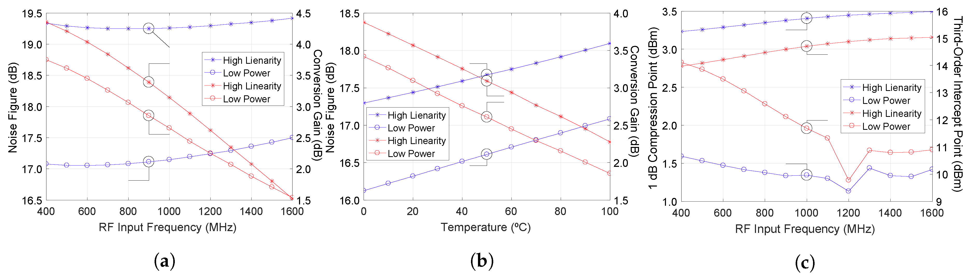
Figure 9 shows the measured operation of the RF mixer in terms of noise figure and gain for a supply of 3
, both for the high-linearity and the low-power modes. In particular,
Figure 9a shows the dependency of these two magnitudes with respect to the RF input frequency in a range from 400
to 1600
, whereas
Figure 9b plots the variation of noise figure and gain with respect to temperature in the desired operation range from 0
to 100
.
Figure 9c shows the values of the 1 dB compression point (P1dB) and the third-order intercept (IP3) of the mixers with respect to the RF input frequency, also for the high-linearity and low-power modes.
Finally,
Table 1 provides a summary of the performance of the main building blocks of the frequency synthesizer, which have been characterized as stand-alone cells: the voltage-controlled oscillators and the mixers. It has to be noted that the figures corresponding to VCO
have been obtained by extracted post-layout simulations, since only VCO
has been fabricated for testing; nevertheless, the synthesizer, which incorporates VCO
has a correct operation over its whole frequency range.
5. Conclusions
This work presents the design and validation of a reconfigurable RF converter for DVB-T television applications. The system is designed to operate in a triple-play architecture over GPON using a carrier at 1550 (third lambda) and spectrum inversion.
By the joint integration of two pairs of frequency synthesizer and mixer, the RF converter in this work takes the DVB-T input, a WDM signal with spectral inversion, formed by 8 channels in the range from 47 –1000 , and up-converts its frequency to the band-pass of a highly selective SAW filter centered at . The resulting signal is subsequently down-converted by the other frequency synthesizer and mixer so that it can be directly input to a television set.
The mixers designed are two double-balanced structures based on the Gilbert cell, with their input RF signals input through the transistor sources for better impedance matching and improved linearity, which can be programmed to operate in a low-power mode or a high-linearity mode. The frequency synthesizer uses two LC-tank VCOs inside an integer-N PLL and a 20 TCXO reference to generate the desired local oscillator signal in a frequency range from to . The system is fed with regulated supplies compensated in temperature and programmed by an IC interface operating on five 16-bit registers.
All in all, the combination of third lambda transmission and spectrum inversion allows operators to alleviate the saturation of the bandwidth in GPONs by broadcasting all traditional television channels using the additional down-link at 1550 , and leaving for IP transmission over the conventional up- and down-links at 1310 and 1490 for premium content requiring added login security. Finally, another advantage of this solution is that the resulting demodulated signal can be fed to any television set without the need for a decoder, facilitating the implementation and use of this service.


