2.1. CMOS Differential Stage with Passive Load
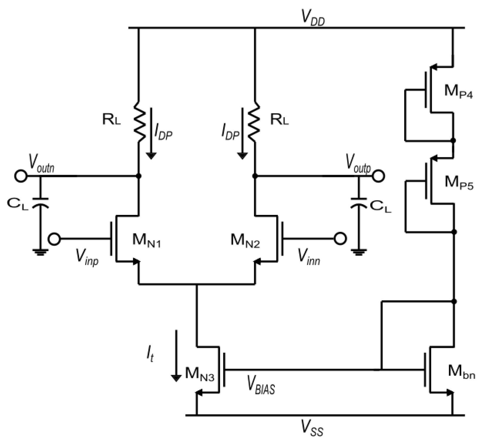
The main objective in designing a CMOS differential stage that is used for the implementation of a VCO, is oriented to achieve the highest oscillation frequency. In this manner, the first task is identifying the design issues to increase the frequency response of the CML block, which is shown in
Figure 1. Its sizing considers that, according to Equation (
1), the oscillation frequency is inversely proportional to both the number of CML stages
N and the propagation delay
. Therefore, to achieve a high oscillation frequency, the delay must be reduced [
16,
18]. It can be approximated by Equation (
2), so that, varying the transistors dimensions [
15,
18,
19], the delay can be reduced by augmenting
and reducing the equivalent capacitance, where
could be the dominant one. On the one hand, augmenting the MOS transistors dimensions leads to larger parasitic capacitance values. Therefore, the sizing is focused on reducing the dimensions of the differential-pair transistors. On the other hand, the load resistance
affects the delay and it also modifies the value of the dominant pole [
20], described as
. In integrated circuit design,
is directly proportional to the gain-bandwidth-product (
), and considering the trade-off between
and the open-loop gain
, the most important issue is enhancing
[
21,
22].
To find the appropriate load resistor value one can use
. If the MOS transistors should be in saturation, one must accomplish
and
. For instance, setting
,
, and
, then
. The overdrive voltages take into account that small size dimensions are desirable, and the ratios are calculated by Equation (
3) that is obtained from the quadratic model equation. In this manner, using CMOS technology of 180 nm from UMC, the sizes are set to
m,
m,
m, and
m.
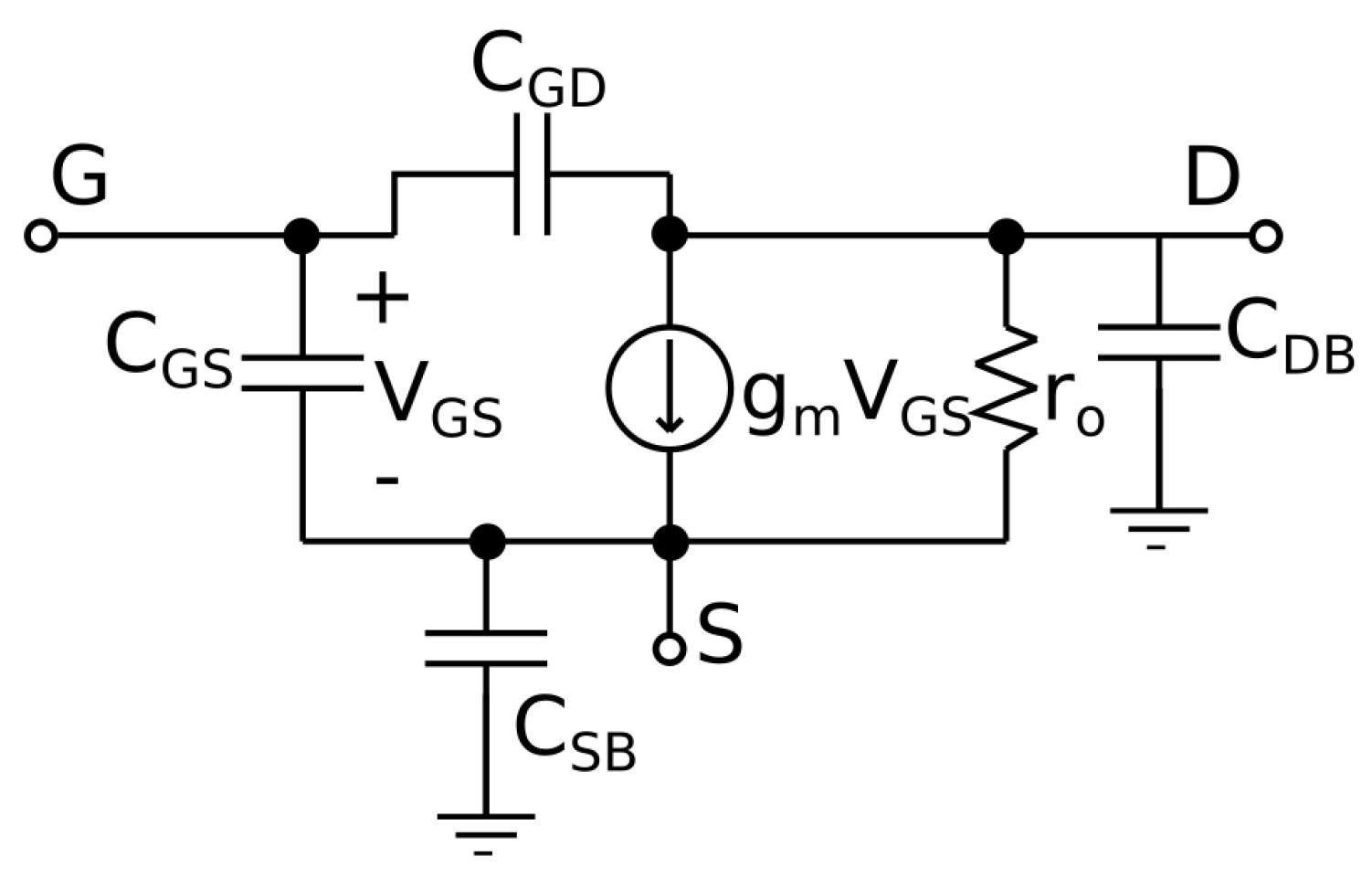
Since the VCO is desired to operate at high frequencies, the MOS high-frequency model shown in
Figure 2 [
22] is used. An input voltage
is connected to the node labeled
, and node
is associated to the sources of the differential pair, so that performing nodal analysis results in the matrix formulation given in Equation (
4), where:
,
,
,
,
,
,
,
,
,
,
,
,
,
. Applying the work in [
23,
24], the compact and second-order symbolic expression that approaches the dominant pole can be expressed by
, where:
and
. It is notorious that the dominant pole value heavily depends on both
and
, the values of which are proportional to the transistor’s sizes [
20]. That way, the reduction of transistor’s sizes leads to an increase of
. To verify the symbolic approximation, the Bode magnitude given in
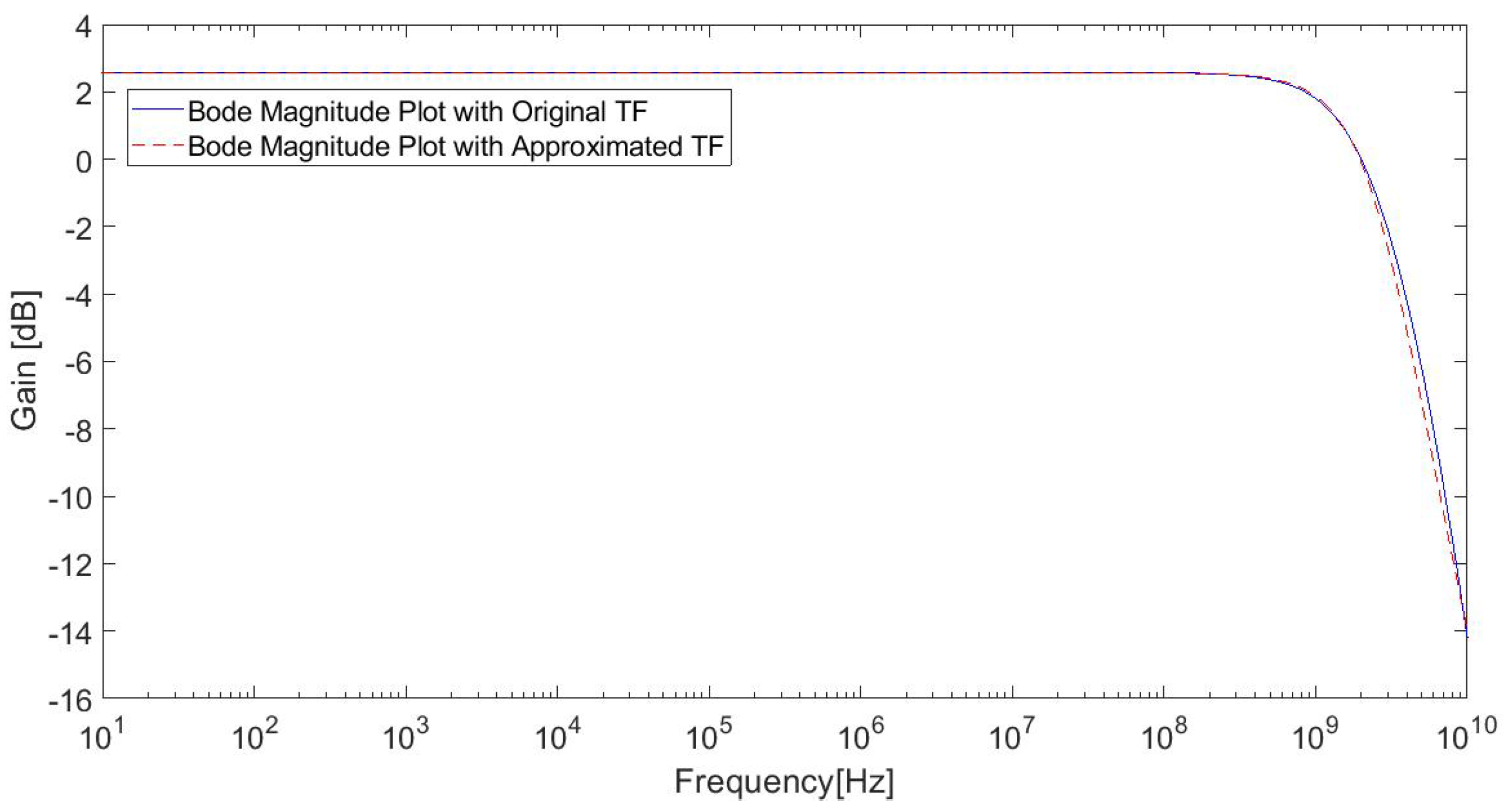
Figure 3 compares the complete or original transfer function (TF) with the approximated TF.
The CMOS CML stage can be characterized measuring the open-loop gain
and the dominant pole
. The gain-bandwidth product
is the frequency at which
becomes 0 dB [
25]. The load capacitor is selected under the supposition that a CML stage must be capable of driving three stages, therefore we assume
, where
is obtained from the .lis file generated from the SPICE circuit simulation. The design is tested under process, voltage and temperature (PVT) variations. A robust design must have a low PVT sensitivity, and it is performed considering five process corners: TT (typical–typical), SS (slow–slow), SNFP (slow–fast), FNSP (fast–slow) and FF (fast–fast). The test considers three voltage variations of
of
, and three temperature variations from
C,
C and
C [
26].
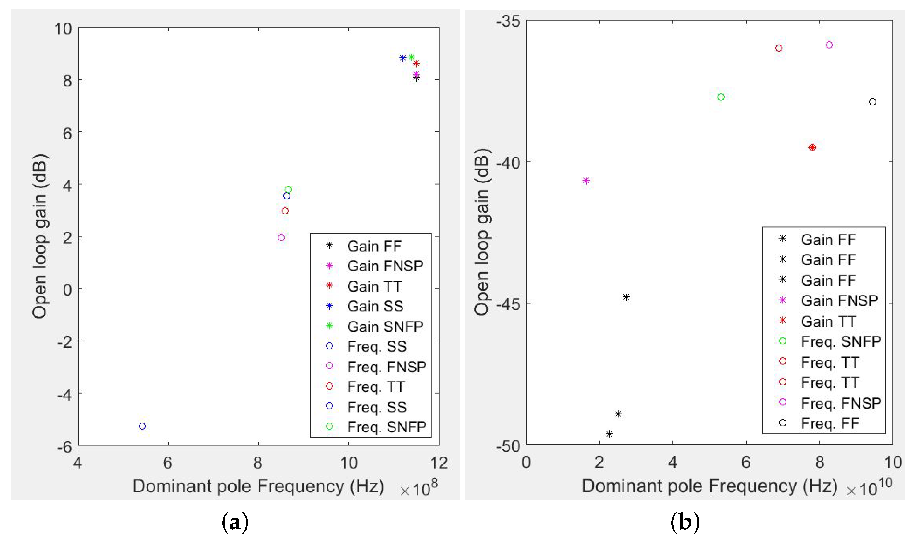
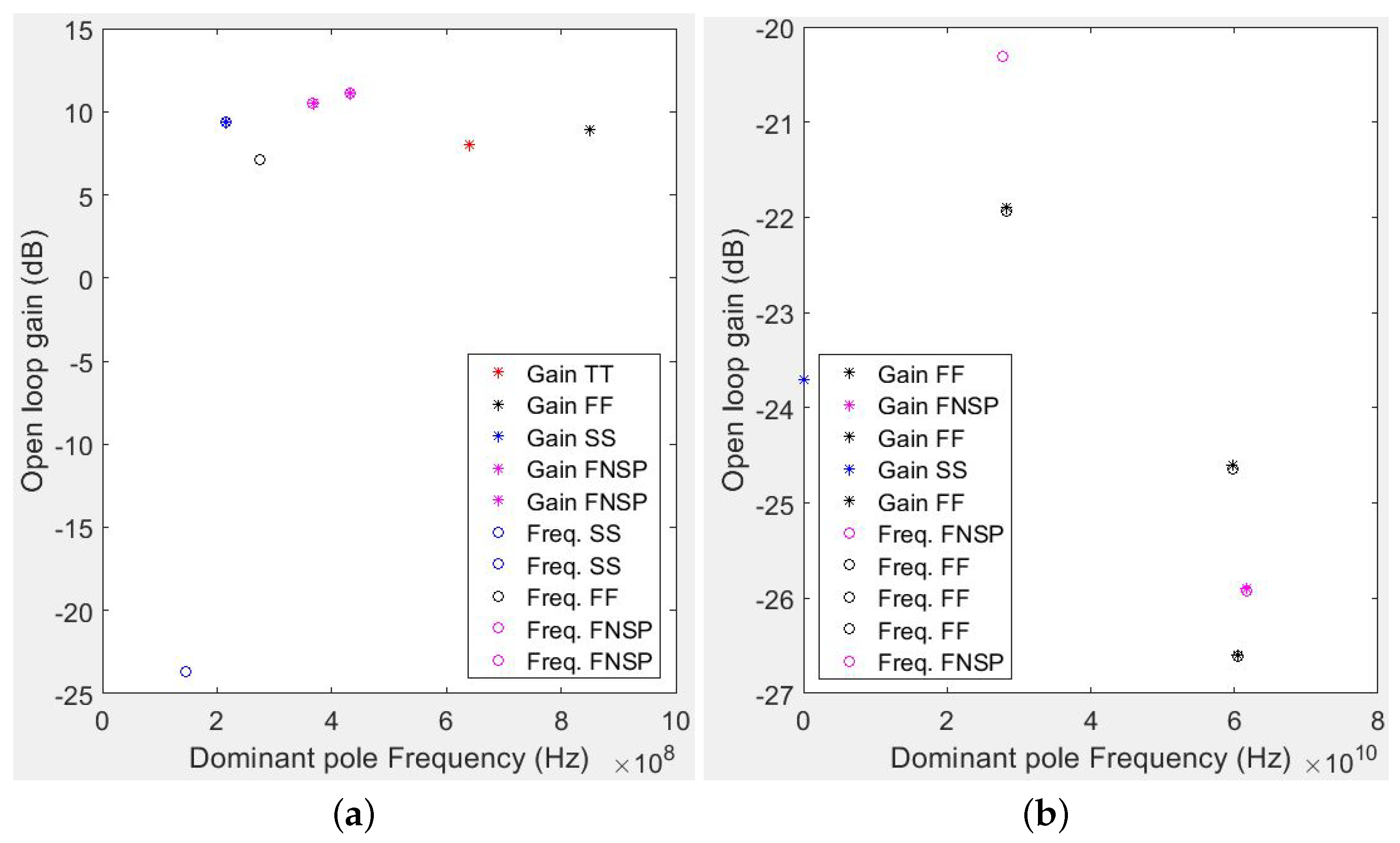
Figure 4 summarizes the higher and lower values resulting from the PVT variations for
. The dependence of the gain and dominant pole values under PVT variations depicted in this figure show that there is a wide variation in both parameters, where the high gain cases occur mostly for lower dominant pole frequencies and viceversa.
Table 1 summarizes the measured
and
values, for each PVT variation. Due to the huge variations, this design is unsuitable for designing a VCO. Therefore, a CMOS CML stage with active load is detailed in the next subsection.
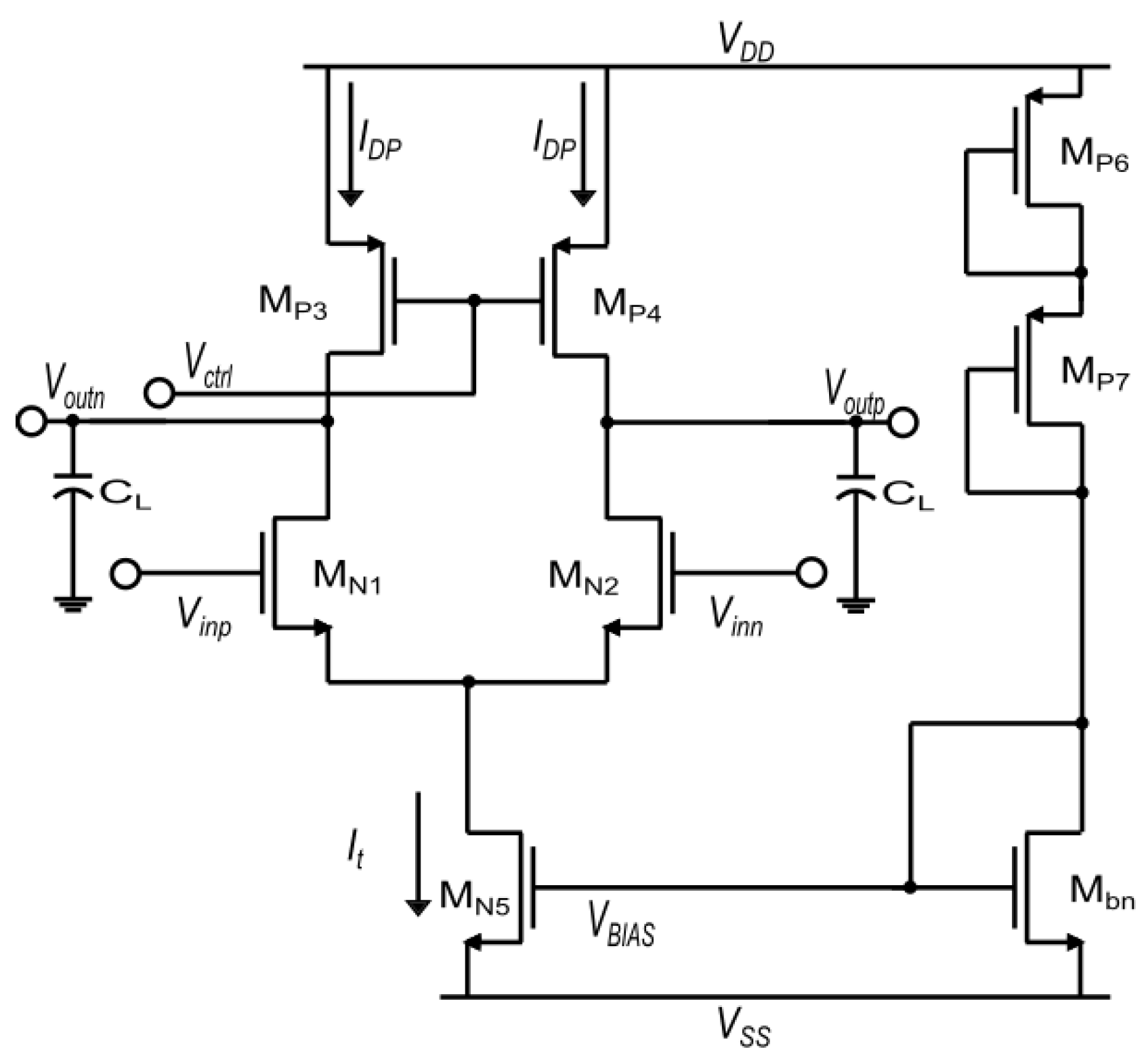
2.2. CMOS Differential Stage with Active Load
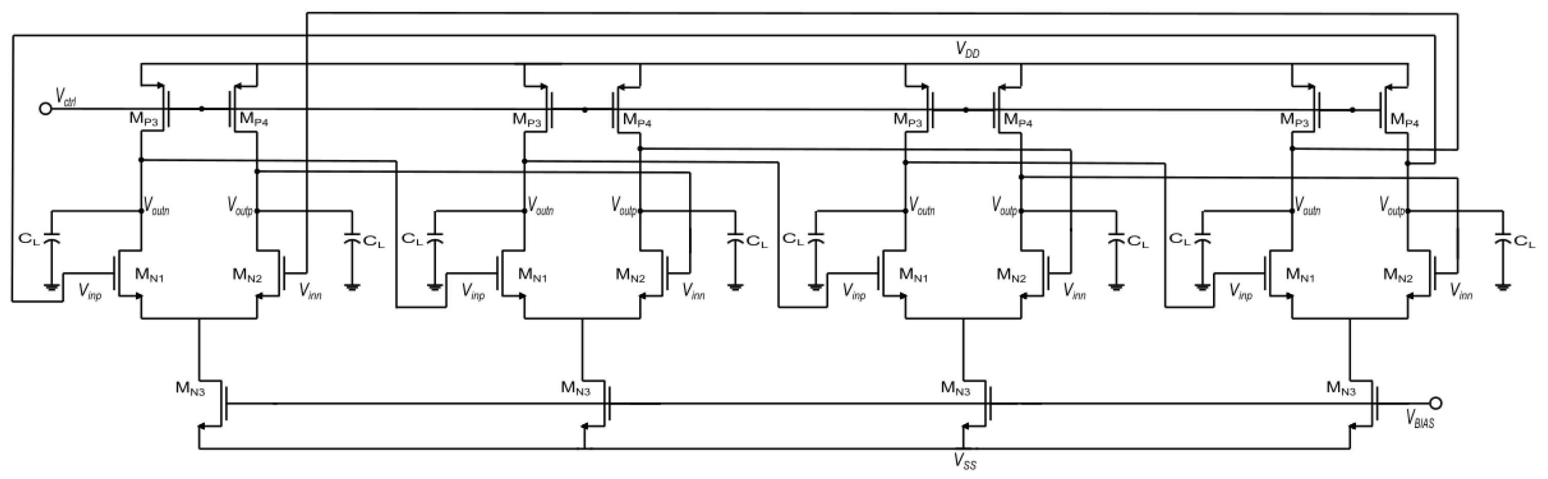
Figure 5 shows the CMOS differential stage with active loads implemented by P-type MOS transistors (
and
) that must operate in the triode region. The value of the equivalent resistance is controlled by varying the voltage at the gates of the PMOS transistors, which is called control voltage
[
16,
27]. The output conductance of the PMOS transistor can be approached as
. The sizing of
-
must accomplish
and Equation (
5) [
28]. To achieve a wide range of control-voltage, the sizes are:
m,
m,
m,
m, and
m, in all cases
m.
The approximation of the dominant pole is performed in the same way as done for the CML stage with passive load, and it can be approached by Equation (
6). The comparison of the Bode magnitude of both the original and the approximated transfer functions (TF) is shown in
Figure 6. Again, it can be appreciated that the dominant pole depends on both
,
of the differential pair, and
of the active load [
24], so that the reduction of the transistor’s sizes leads to an increase of
.
The characterization of the CMOS differential stage with active load provides the results given in
Section 4, where one can see the comparison between the performances with and without post-layout simulations. The PVT variations are simulated setting
, considering five process corners (TT, SS, SNFP, FNSP and FF), three voltage variations (
of
), and three temperature variations (
C,
C and
C) [
26]. The higher and lower gain and frequency values are shown in
Figure 7. One can see that the higher dominant pole frequencies are achieved in the FNSP and TT process corners; however, the FNSP corner also presents some of the lowest dominant pole values along with the SS corner.
Table 2 summarizes the PVT simulation results.
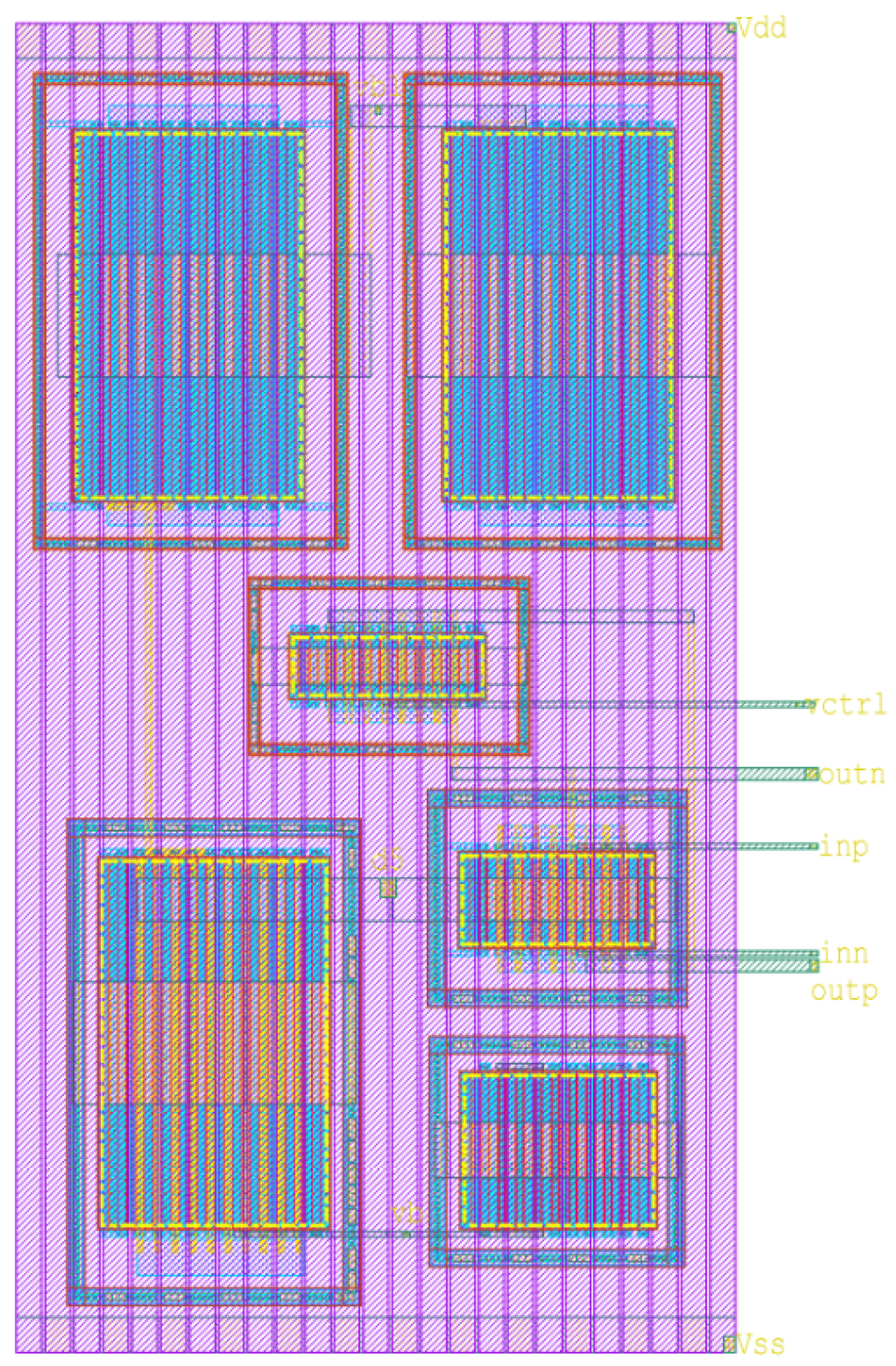
2.3. Voltage Controlled Oscillator Based on CMOS Differential Stages
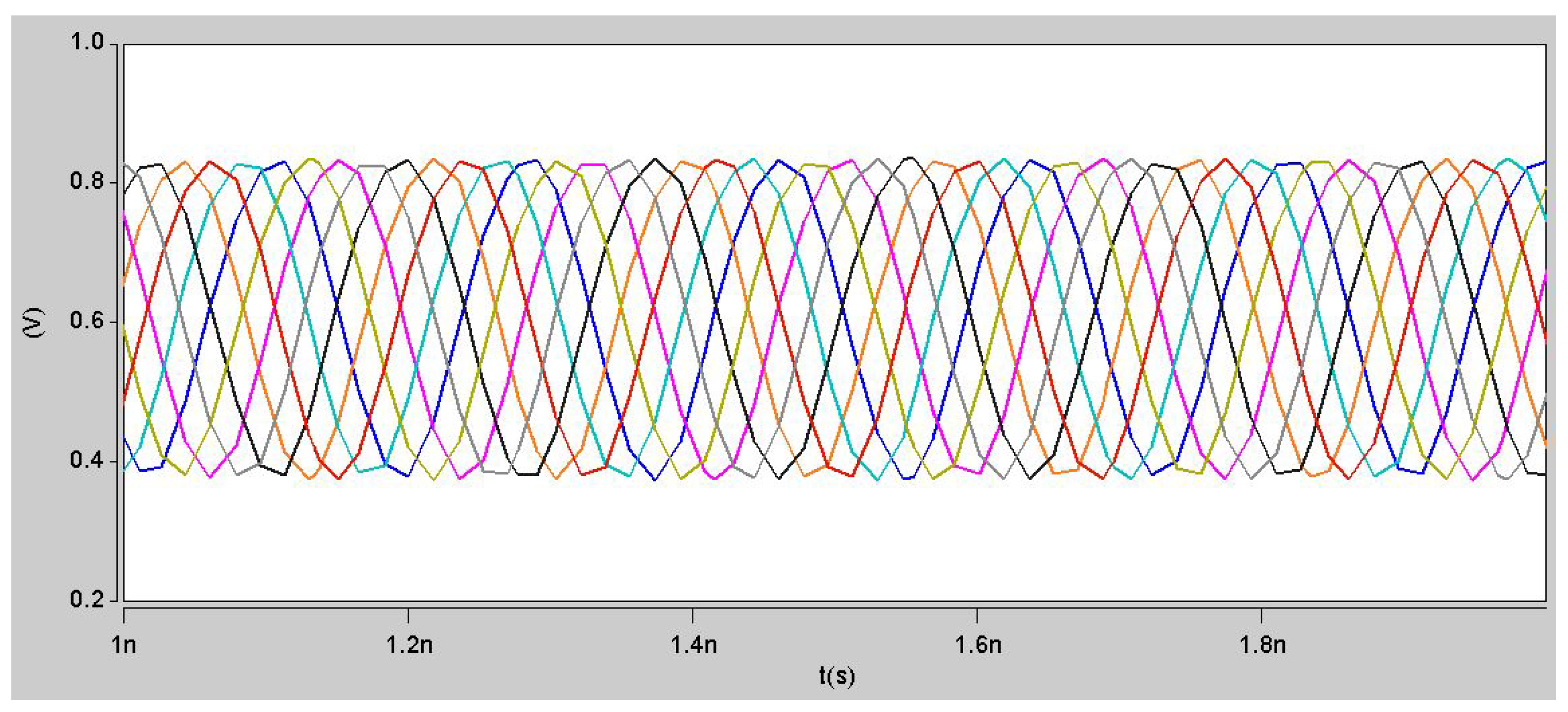
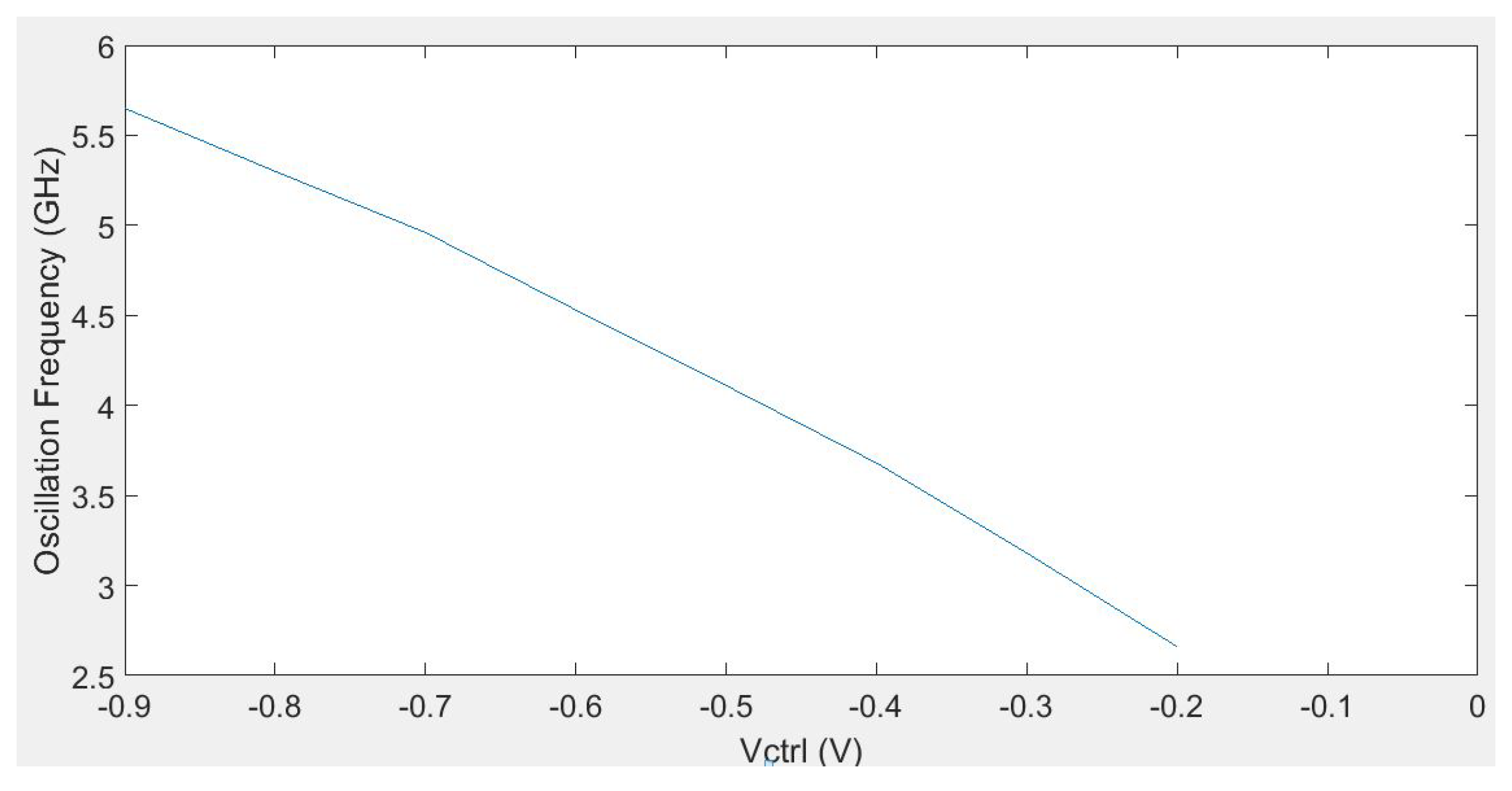
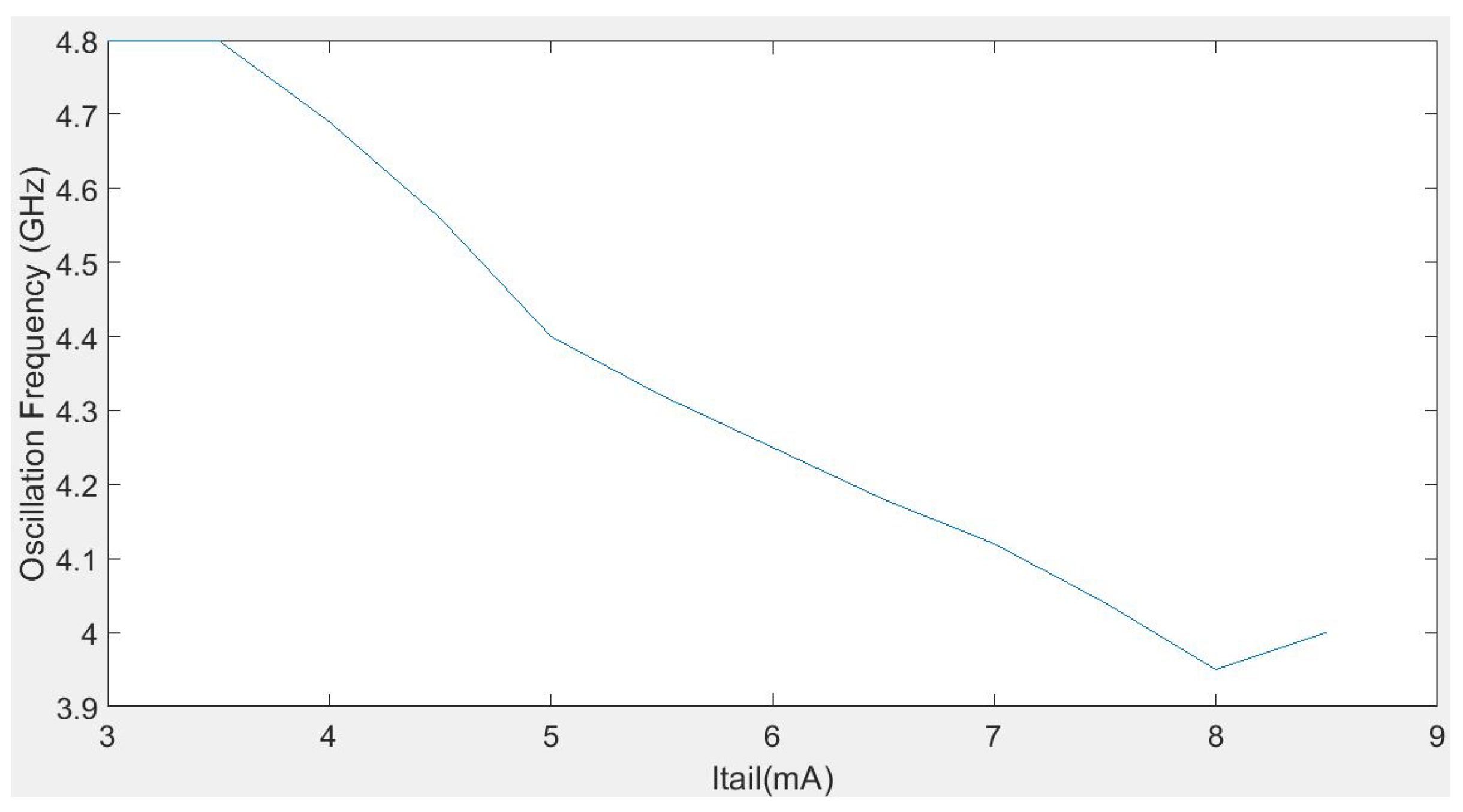
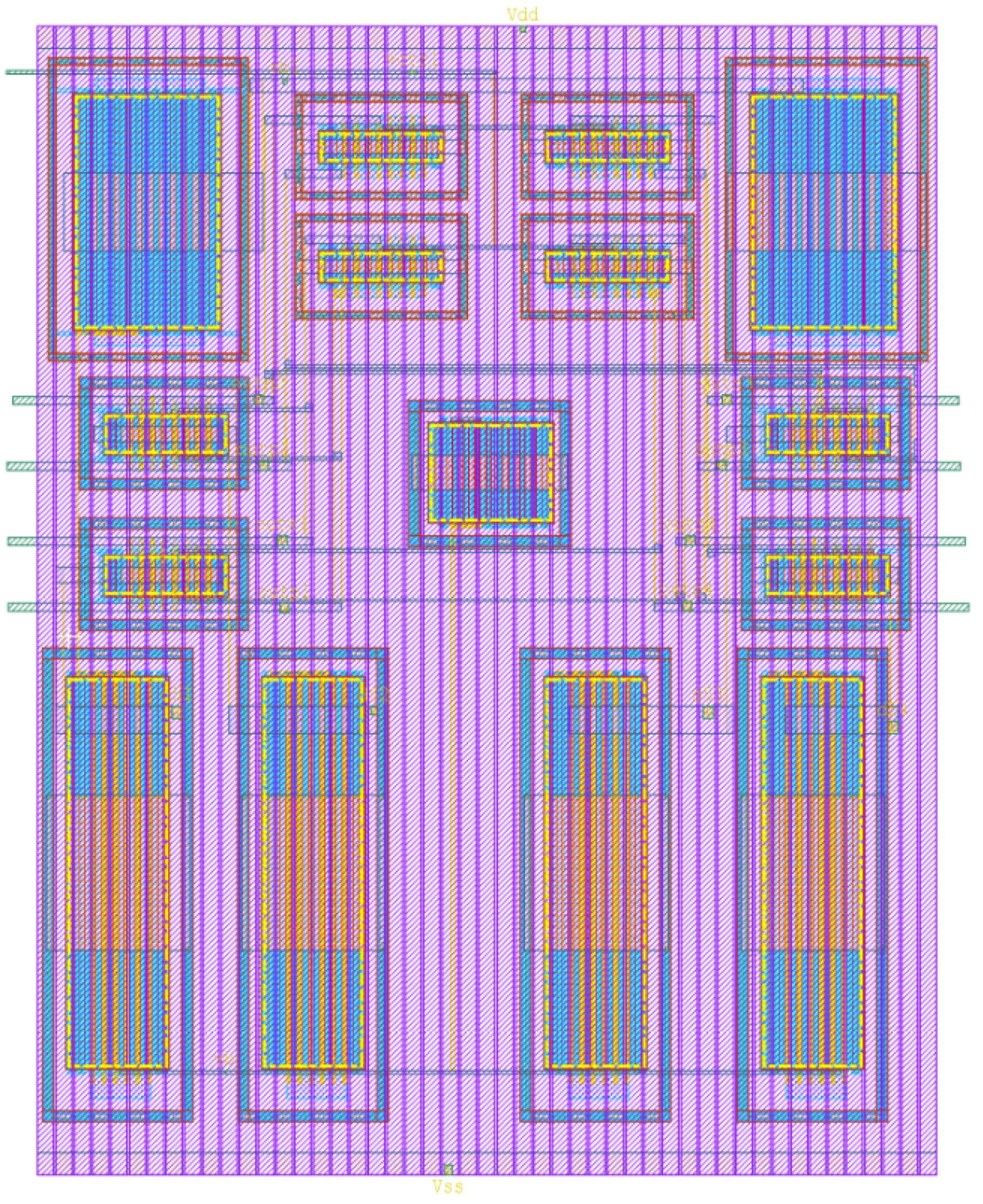
The CMOS differential stage with active load is used herein to design a four-differential stages VCO, as shown in
Figure 8. In this case, the sizes of the MOS transistors are varied to reach the highest oscillation frequency, so that they were established as
m,
m, with
, thus resulting in oscillations between the frequencies 2.65 GHz and 5.65 GHz, which require control voltages in the range between
V and
V. The oscillating frequency of 5.65 GHz with a control voltage of
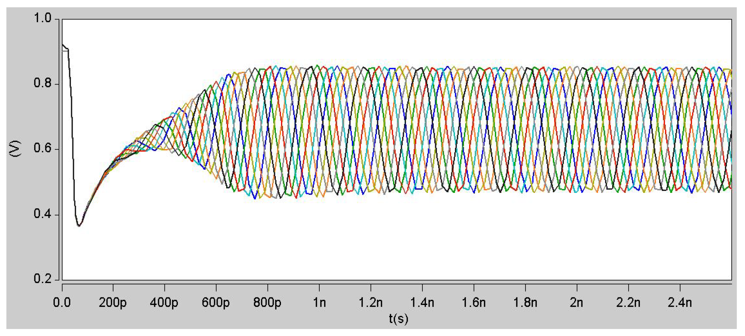
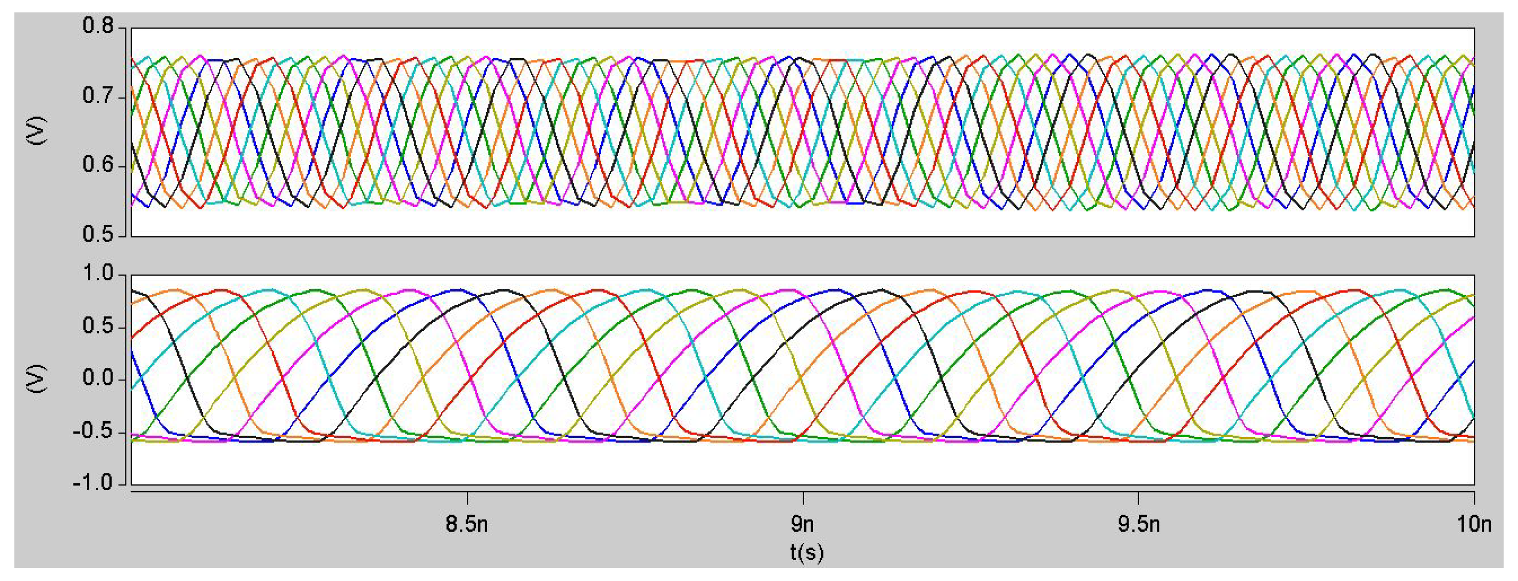
V is shown in
Figure 9, for which the average power consumption was 39 mW. The control voltage range can be appreciated in
Figure 10.
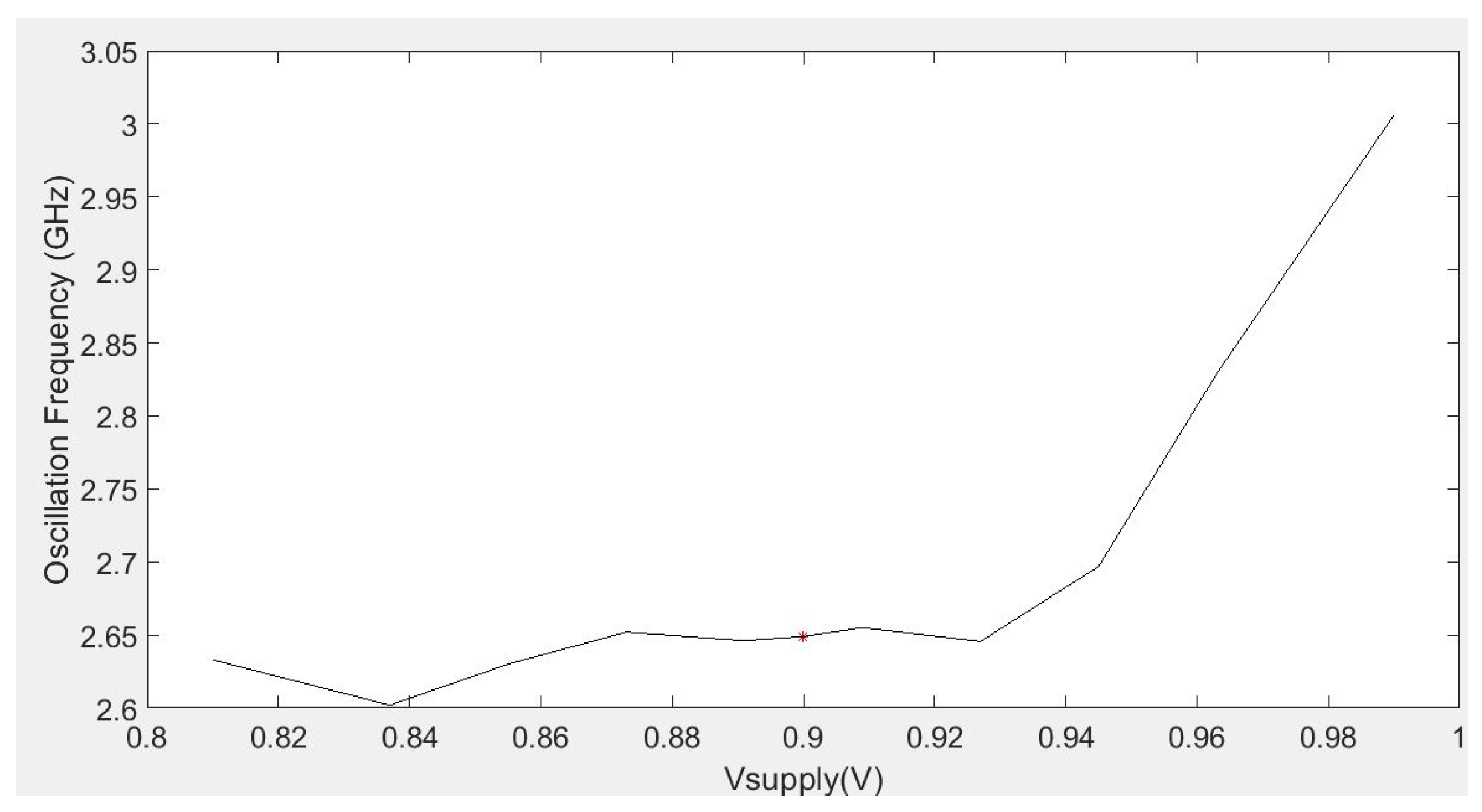
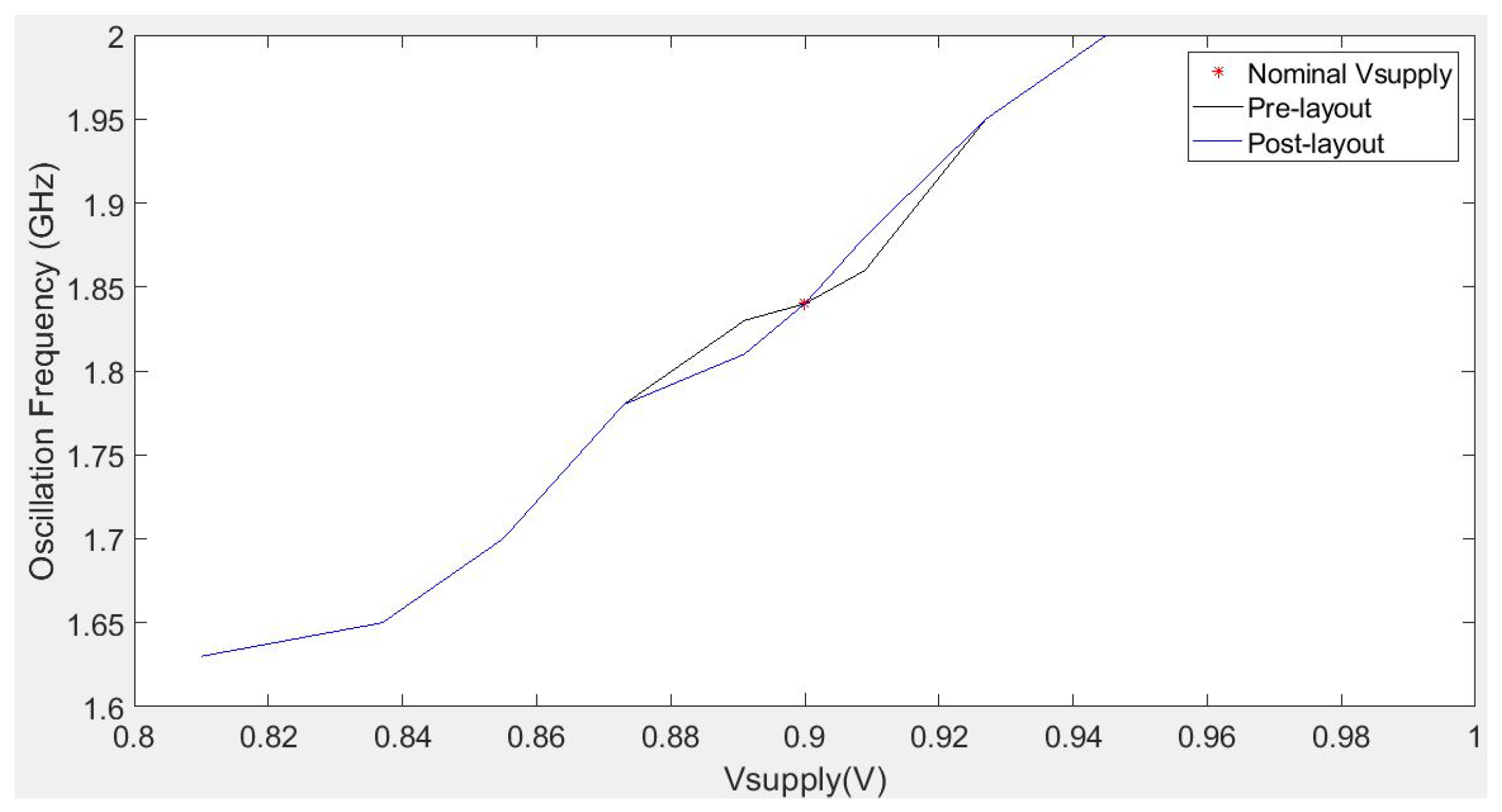
The static supply sensitivity of the VCO is very important, and it is measured observing the change in the oscillation frequency due to a
supply voltage variation [
29].
Figure 11 shows the frequency variations produced by the changes in the supply voltage. The results show a static supply sensitivity of
.
Table 3 shows a comparison between the proposed VCO and other CML-based VCOs already published in the literature. As one can see, the three VCOs are designed using CMOS technology of 180 nm and voltage supplies of 1.8 V. Other VCOs implemented in CML-based ring structure have been designed and applied in analog-to-digital converter [
30] and pseudo-random bit sequence generator [
31]. However, they are not listed in
Table 3 due to lack of information such as number of stages, supply voltage, tail current, load capacitance, and power dissipation. Besides, the VCO in [
30] was implemented using CMOS technology of 90 nm and the one in [
31] using 180 nm. These VCOs provide frequency tuning ranges of 1–7.2 and 2.7–3.3 GHz and voltage tuning ranges of 0.32–0.62 and 0–1.1 V, respectively. On the other hand, the proposed VCO uses four stages and a higher load capacitance compared to the one in [
15,
32], and it provides the higher frequency tuning range while maintaining an acceptable control-voltage range, power dissipation and supply sensitivity.

 ,
, 


