Abstract
Partial shading on photovoltaic (PV) strings consisting of multiple panels connected in series is known to trigger severe issues, such as reduced energy yield and the occurrence of multiple power point maxima. Various kinds of differential power processing (DPP) converters have been proposed and developed to prevent partial shading issues. Voltage stresses of switches and capacitors in conventional DPP converters, however, are prone to soar with the number of panels connected in series, likely resulting in impaired converter performance and increased circuit volume. This paper proposes a DPP converter using an LLC resonant voltage multiplier (VM) with a voltage divider (VD) to reduce voltage stresses of switches and capacitors. The VD can be arbitrarily extended by adding switches and capacitors, and the voltage stresses can be further reduced by extending the VD. Experimental verification tests for four PV panels connected in series were performed emulating partial shading conditions in a laboratory and outdoor. The results demonstrated the proposed DPP converter successfully precluded the negative impacts of partial shading with mitigating the voltage stress issues.
1. Introduction
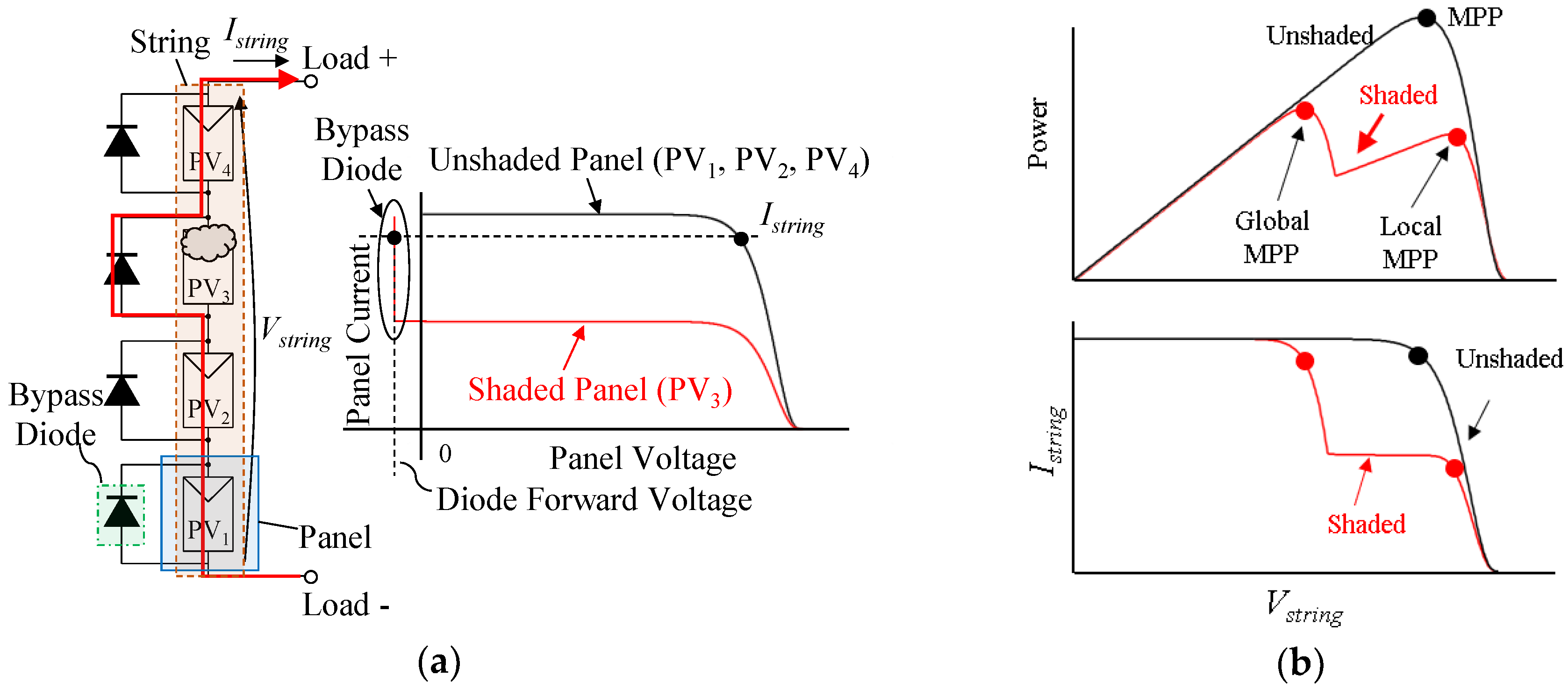
Ordinary photovoltaic (PV) panels generally consist of two or three substrings, each comprising multiple cells connected in series. PV panels are further connected in series to meet voltage requirements of loads or systems. When partial shading occurs on the series-connected PV panels due to neighboring buildings, fallen leaves, bird dropping, etc., electrical characteristics of series-connected PV substrings or panels (hereafter call panels unless otherwise noted) are mismatched. Characteristic mismatch conditions are also triggered by uneven aging of panels and uneven irradiance due to curved surfaces of PV panels. Under characteristic mismatch conditions, a string current, Istring, flows through a bypass diode that is connected in parallel with a shaded panel, as illustrated in Figure 1a. The bypassed panel no longer generates power as its voltage is subzero value, significantly reducing the power generation of the string as a whole. An annual energy yield reportedly deteriorates by 20%–30% due to partial shading on a PV panel [1]. Furthermore, partial shading generates multiple maximum power points (MPPs), including one global and some local MPPs, on a P–V characteristic of the partially-shaded string that might hinder and confuse ordinary MPP tracking (MPPT) algorithms—the shaded PV panel might operate at a local MPP, at which the panel generates less power than at the global MPP, as shown in Figure 1b. Although advanced MPPT techniques have been proposed to certainly track the global MPP even under partial shading conditions [2], a shaded panel is bypassed and cannot contribute to power generation, unavoidably resulting in reduced energy yield.
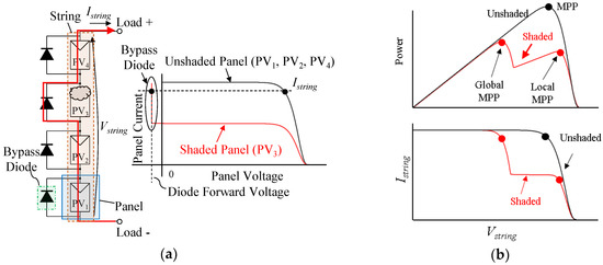
Figure 1.
Characteristics under partial shading conditions: (a) Current path and panel characteristics; (b) String characteristics.
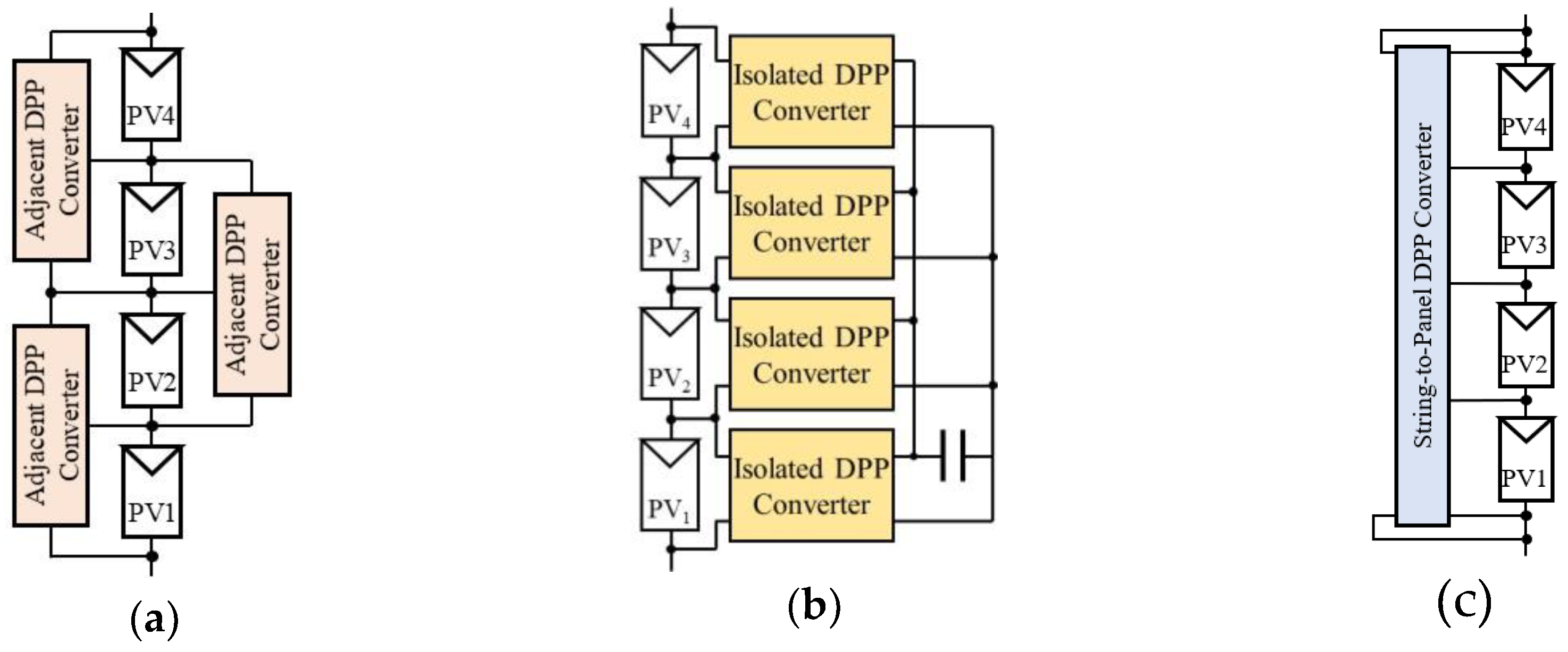
Various kinds of differential power processing (DPP) converters, also known as voltage equalizers, have been proposed and developed. DPP converters deliver power from unshaded panels to shaded ones so that all panel characteristics are virtually matched to preclude the abovementioned partial shading issues. DPP converters are roughly categorized into three groups based on power redistribution scenarios, as shown in Figure 2: the adjacent panel-to-panel architecture, panel-to-panel architecture with an isolated port, and string-to-panel architecture. DPP converters in the adjacent panel-to-panel architecture are based on nonisolated bidirectional converters, such as PWM converters [3,4,5,6,7,8,9,10] and switched capacitor converters [11,12,13,14,15,16,17]. Isolated bidirectional flyback converters are employed in the panel-to-panel architecture with an isolated port [18,19,20,21,22,23,24]. For the string-to-panel architecture, single-input–multi-output converters, such as a multi-winding flyback converter [25], multi-stacked buck-boost converters [26,27], and resonant voltage multipliers (VMs) [28,29,30,31], are employed. Regardless of types of architectures, these DPP converters transfer a fraction of the generated power of unshaded panels to shaded ones so that all panel characteristics are virtually matched.

Figure 2.
Differential power processing (DPP) architectures: (a) Adjacent panel-to-panel architecture; (b) Panel-to-panel with isolated port architecture; (c) String-to-panel architecture.
In PV systems, more than ten panels are connected in series to form a PV string, and an MPP voltage and open-circuit voltage of such strings reach 400–600 V for traditional systems or even 1000 V for the latest high-voltage PV systems. With the adjacent panel-to-panel architecture, shown in Figure 2a, numerous DPP converters in proportion to the number of series-connected panels necessary, and therefore the total volume, cost, and complexity of the system as a whole are prone to increase. Furthermore, since power transfer is limited only between adjacent two panels, power from unshaded panels might have to traverse multiple DPP converters and panels before reaching shaded panels, hence collectively increasing power conversion losses. With the panel-to-panel architecture with an isolated port, shown in Figure 2b, power from unshaded panels can directly be transferred to shaded ones via the isolated port. However, each DPP converter contains a bulky and expensive transformer, and the number of DPP converters necessary is equal to the number of panels connected in series, thus resulting in increased system complexity and cost. Meanwhile, the number of DPP converters can be ideally reduced to only one in the string-to-panel architecture, as shown in Figure 2c. Furthermore, shaded panels can directly receive power from the string, and hence the overall power conversion efficiency can be improved in comparison with the adjacent panel-to-panel architecture.
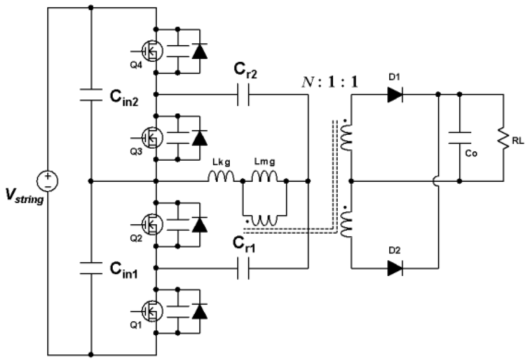
Conventional DPP converters have been chiefly developed for substring-level equalization within individual panels, and therefore voltage stresses of semiconductor devices and passive components are rated for panel voltages around 30–50 V. For panel-level equalization, on the other hand, circuit components are exposed to a string voltage Vstring of several hundred volts. Three-level converters based on a neutral-point diode-clamped converter [32] and an LLC resonant converter (see Figure 3) [33] have been proposed to mitigate voltage stress issues, and voltage stresses of switches and capacitors can be reduced to Vstring/2. However, these circuit components are still exposed to high voltage stresses in high-voltage PV strings.
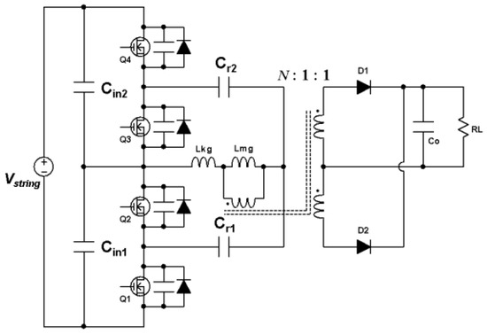
Figure 3.
Three-level LLC resonant converter.
This article presents a novel DPP converter for the string-to-panel DPP architecture for high-voltage strings. The proposed DPP converter is based on the combination of a conventional LLC resonant VM and voltage divider (VD) using switched capacitor converters (SCCs). In comparison with the conventional DPP converter based on the LLC resonant VM, voltage stresses of switches can be reduced. In addition, voltage stresses of input smoothing capacitors can also be reduced by adding inductors to the SCCs. The rest of this paper is organized as follows. Section 2 discusses the proposed DPP converter and its major features. The operation analysis will be performed in Section 3. Section 4 presents the results of experimental verification tests using a prototype for four or eight panels connected in series in a laboratory and outdoor. Section 5 contains the concluding statements.
2. Proposed DPP Converter Based on Voltage Divider and LLC Resonant Voltage Multiplier
2.1. Key Circuits for Proposed DPP Converter
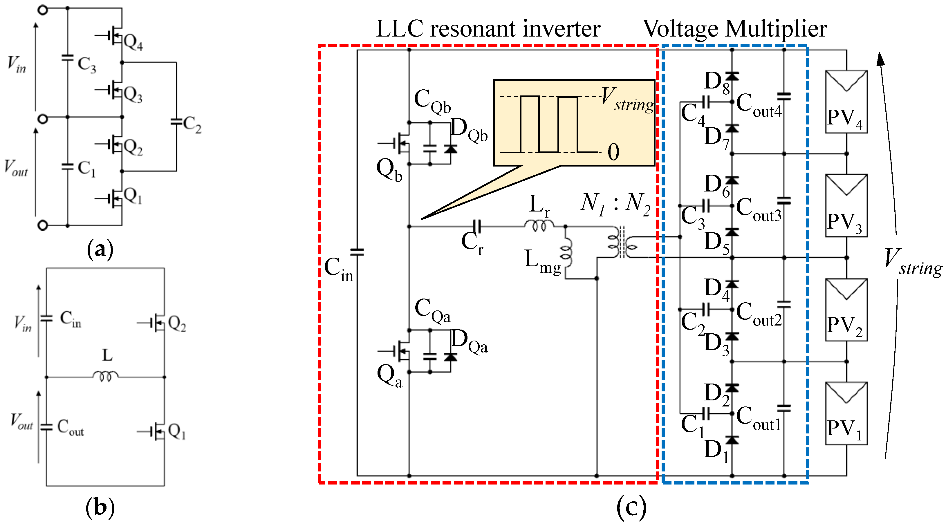
From three key circuits of an SCC, bidirectional PWM converter, and conventional LLC resonant VM (see Figure 4), the proposed DPP converter for the string-to-panel architecture can be derived. Switches in the SCC (see Figure 4a) are driven with a fixed 50% duty cycle, and all capacitors in the SCC are indirectly connected in parallel, and their voltages are automatically balanced. With the bidirectional PWM converter operating with a fixed 50% duty cycle (see Figure 4b), the voltages of the input and output capacitors, Cin and Cout, can be automatically balanced.
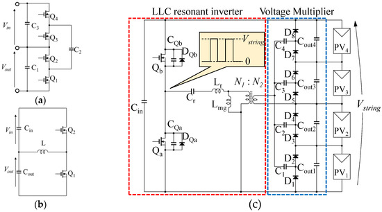
Figure 4.
Key circuits for proposed DPP converter: (a) Switched capacitor converter (SCC); (b) Bidirectional PWM converter; (c) LLC resonant voltage multiplier (VM).
The LLC resonant VM, shown in Figure 4c, comprises an LLC resonant inverter and VM. The high- and low-side switches (Qb and Qa) are driven at a fixed frequency with a fixed 50% duty cycle in a complementary manner, and the LLC resonant tank is driven by a square-wave voltage with a peak-to-peak voltage of Vstring, as shown in the inset of Figure 4c. A sinusoidal current generated by the LLC resonant tank is transferred to the secondary side and is rectified by the VM. Eventually, the VM produces uniform multiple output voltages, by which PV substring characteristics are automatically unified even without feedback control [28,29,30,31].
2.2. Proposed DPP Converter
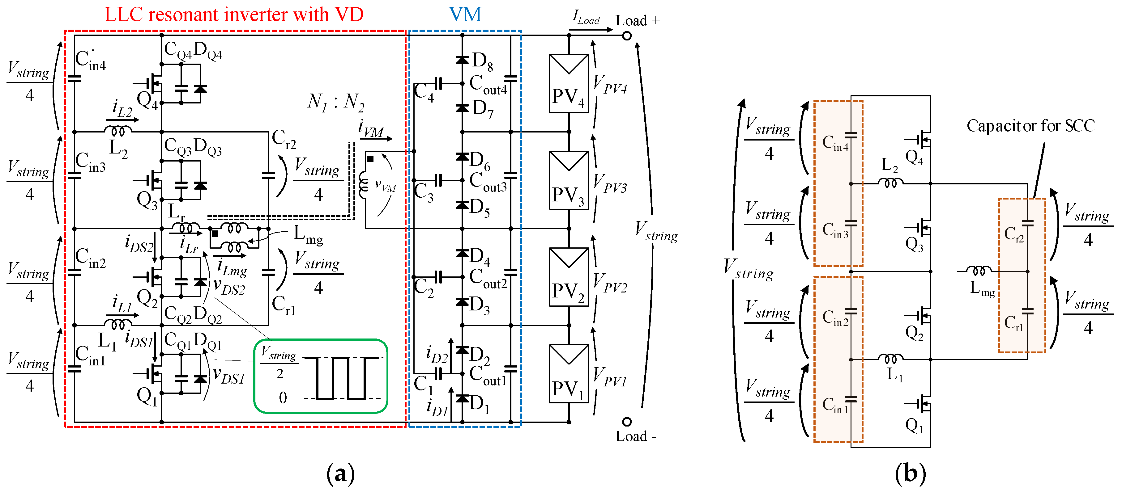
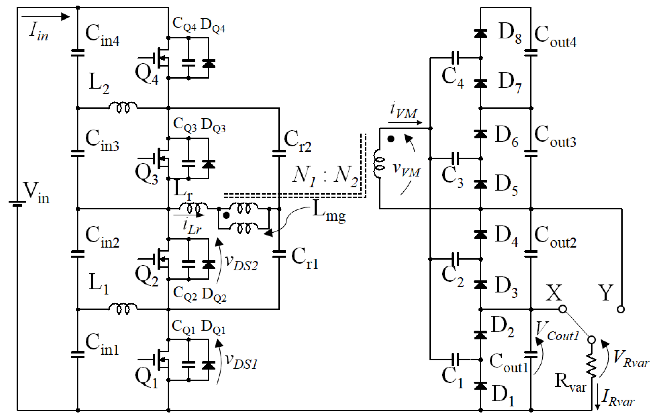
By merging the three circuits shown in Figure 4, the proposed DPP converter for the string-to-panel architecture can be derived, as shown in Figure 5a, in which a topology for four panels connected in series is exemplified. In comparison with the conventional DPP converter shown in Figure 4c, the VM is identical, whereas the LLC resonant inverter side is modified to be a VD with an LLC resonant inverter to reduce voltage stresses of switches Q1–Q4 and input smoothing capacitors Cin1–Cin4. Body diodes (DQ1–DQ4) and parasitic output capacitances (CQ1–CQ4) of MOSFETs, which play important roles to achieve zero voltage switching (ZVS) operations, are also illustrated. A leakage inductance Lr and magnetizing inductance Lmg of the transformer are utilized for the resonant operation. The VD comprises the SCC containing inductors, while the LLC resonant inverter is very similar to that in the conventional DPP converter shown in Figure 4c. For the sake of clarity, the circuit on the VD side is defined as a transformer’s primary side, and the secondary side is the VM. The string voltage Vstring is divided into four by the SCC and PWM converters in the VD, achieving the reduced voltage stresses of circuit components on the primary side.
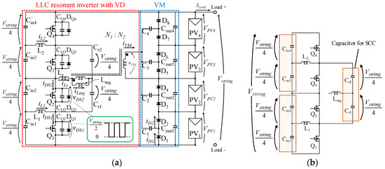
Figure 5.
(a) Proposed DPP converter based on voltage divider (VD) and LLC resonant voltage multiplier (VM); (b) Voltage divider.
The VD circuit is emphasized in Figure 5b. Series-connected capacitors (i.e., Cin1–Cin2, Cin3–Cin4, and Cr1–Cr2) act as capacitors C1, C2, and C3 in the traditional SCC (see Figure 4a), respectively. Cr1 and Cr2 also behave like resonant capacitors. Meanwhile, thanks to the added inductors of L1 and L2, and the magnetizing inductor Lmg of the transformer, three PWM converters can be formed in the VD. By driving switches with a fixed 50% duty cycle, all capacitor voltages are automatically balanced to be Vstring/4 by the SCC and PWM converters in the VD.
The LLC resonant VM is driven by the VD. Resonant capacitors, Cr1 and Cr2, and Lmg form an LLC resonant tank that produces ac current and voltage. The ac power generated by the LLC resonant tank is transferred to the secondary side, and the transferred power is automatically redistributed to shaded panels having weak characteristics. This power redistribution realizes automatic characteristic equalization. The detailed operation principle and mechanism of this power redistribution have been reported and discussed in detail in the past work [28].
2.3. Major Features
Similar to the conventional LLC resonant VM, a fraction of the generated power of the string is automatically transferred to the shaded panel(s) through the proposed DPP converter even without feedback control. In other words, the proposed DPP converter can operate with a fixed duty cycle at a fixed switching frequency, and no voltage and current sensing are necessary. This automatic power redistribution allows eliminating a feedback control loop from the DPP converter, achieving simplified circuit implementation.
The voltage stresses of switches and capacitors on the primary side can be reduced in comparison with the conventional LLC resonant VM (see Figure 4c). The reduced voltage stresses of capacitors allow small multi-layer ceramic capacitors (MLCCs) to be used even for high-voltage applications. Although multiple inductors are necessary for the VD, these inductors can be very tiny as their average currents are zero.
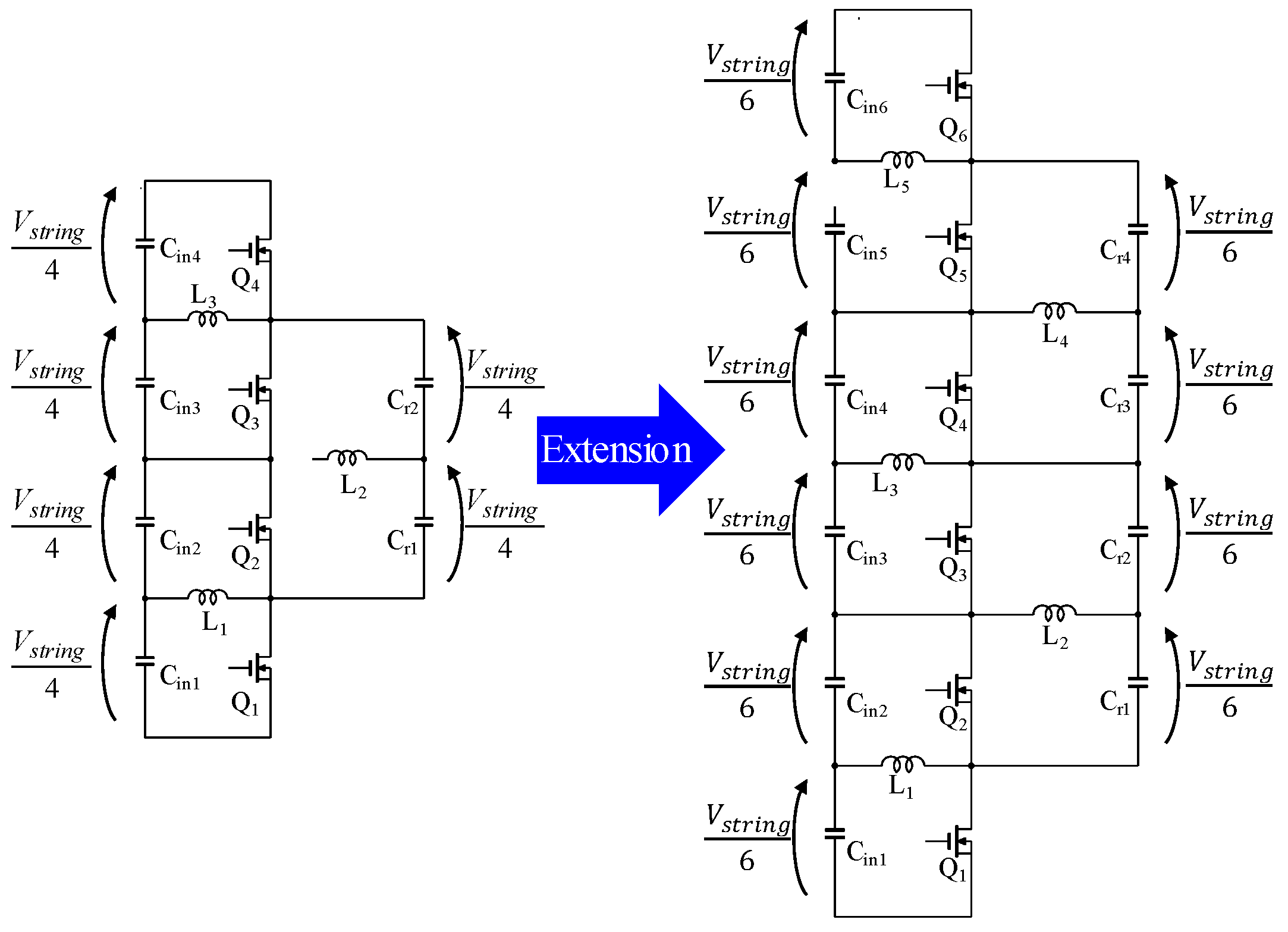
Another feature of the proposed DPP converter is that the VD is scalable. The VD in the proposed DPP converter can be arbitrarily extended by adding capacitors, switches, and inductors. The larger the number of circuit components in the VD, the lower will be the voltage stresses of capacitors and switches. Figure 6 illustrates the scalability of the VD. The left-hand side circuit consists of four input capacitors connected in series (defined as n = 4), and voltage stresses of capacitors and switches are Vstring/4 and Vstring/2, respectively. The circuit on the right-hand side corresponds to the case of n = 6, and voltage stresses of capacitors and switches can be reduced to Vstring/6 and Vstring/3, respectively. Either L2 or L4, or both of them, is replaced with a magnetizing inductance of a transformer to form an LLC resonant VM. Similarly, by extending the circuit to n = 8, the voltage stresses of capacitors and switches can be further reduced to Vstring/8 and Vstring/4.
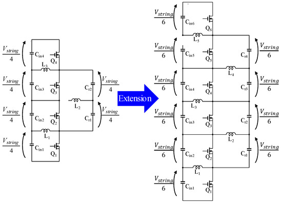
Figure 6.
Extension of VD from n = 4 to n = 6.
2.4. Extended Topology of Proposed DPP Converter
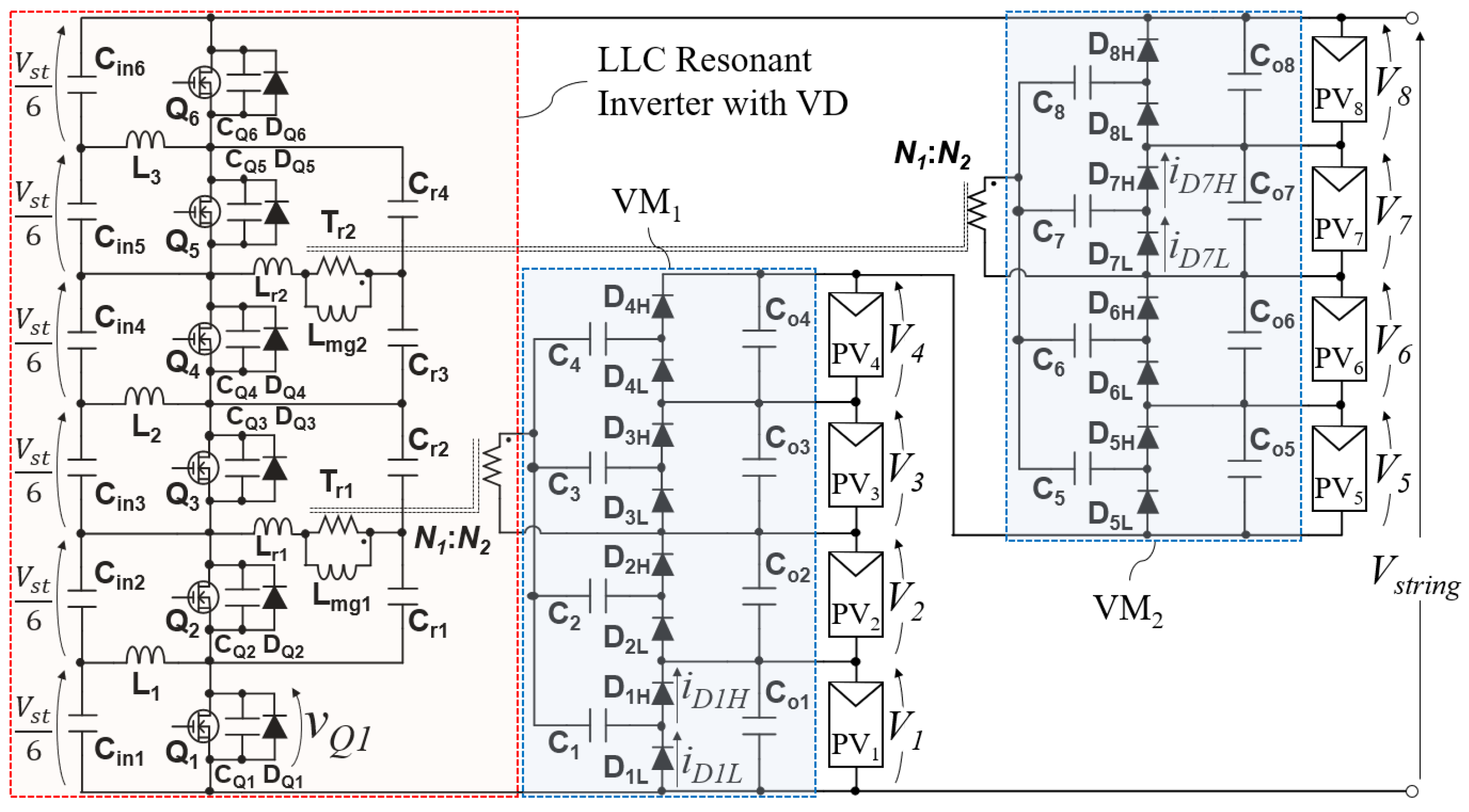
An extended version of the proposed DPP converter is exemplified in Figure 7. This topology is the combination of a VD with n = 6 (see Figure 6) and two LLC resonant VMs (VM1 for PV1–PV4, and VM2 for PV5–PV8). Vstring is divided into six in the VD, allowing reduced voltage stresses of capacitors and switches, as mentioned in Section 2.3. L2 and L4 in the VD in Figure 6 are replaced with transformers’ magnetizing inductances, Lmg1 and Lmg2, respectively. An operation mechanism of VMs in the extended topology is identical to that of the VM in Figure 5a. Hence, in the next section, the operation analysis is performed only for the basic topology for the sake of clarity.
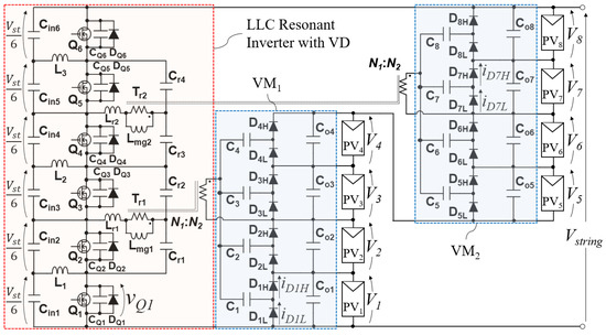
Figure 7.
Extended DPP Converter using two VMs and VD with n = 6.
The increased design difficulty should be cited as a drawback of the proposed DPP converter. The conventional DPP converters for the adjacent panel-to-panel architecture (Figure 2a) and panel-to-panel with an isolated port architecture (Figure 2b) are fully modular and can be applied to any numbers of panels connected in series without design changes. The proposed DPP converter, on the other hand, needs to be redesigned by properly designing the transformers, VD, and VM as the number of panels connected in series changes.
3. Operation Analysis
3.1. Operation Principle
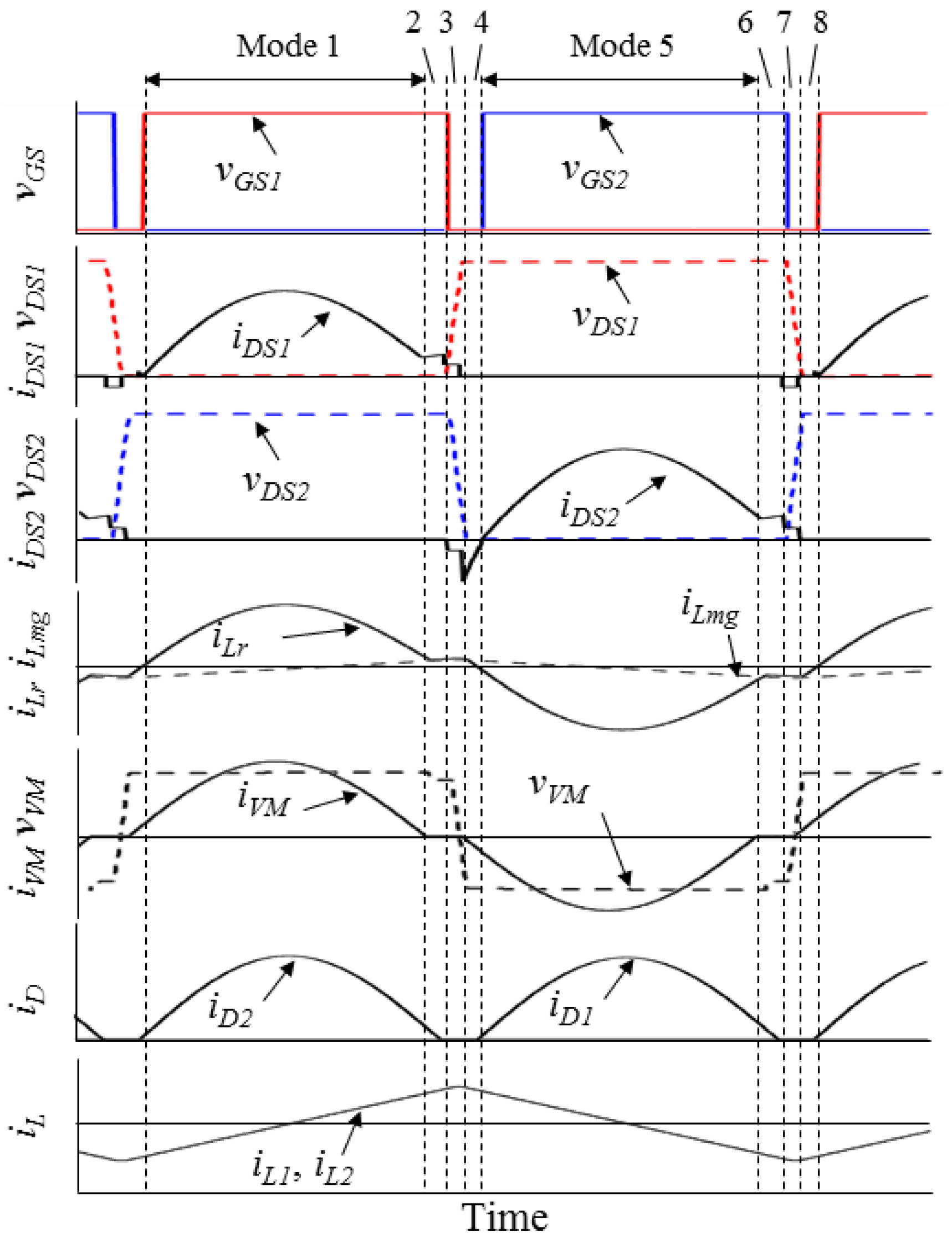
The operation analysis is performed for the case that PV1 only is partially shaded. Key operation waveforms and current flow paths are shown in Figure 8 and Figure 9, respectively. All switches are driven with a fixed duty cycle with a proper dead time period. Current and voltage waveforms of Q1 and Q2 are identical to those of Q4 and Q3, and therefore, waveforms of Q1 and Q2 only are illustrated and discussed in this section. Capacitances of the resonant capacitors of Cr1 and Cr2 are assumed identical.
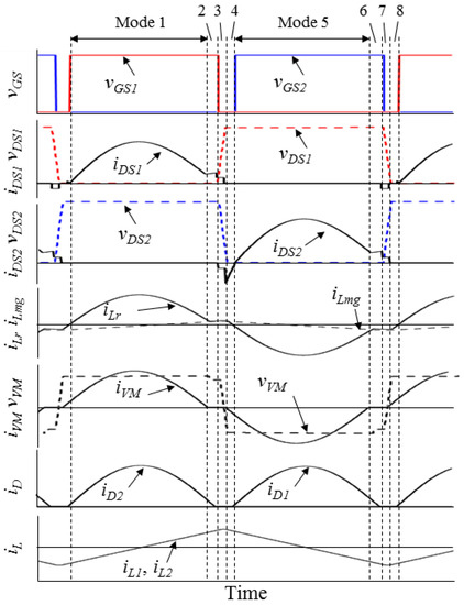
Figure 8.
Theoretical key operation waveforms when PV1 is shaded.
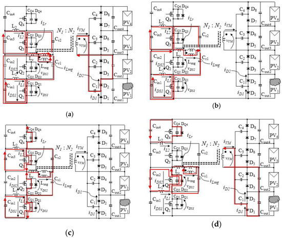
Figure 9.
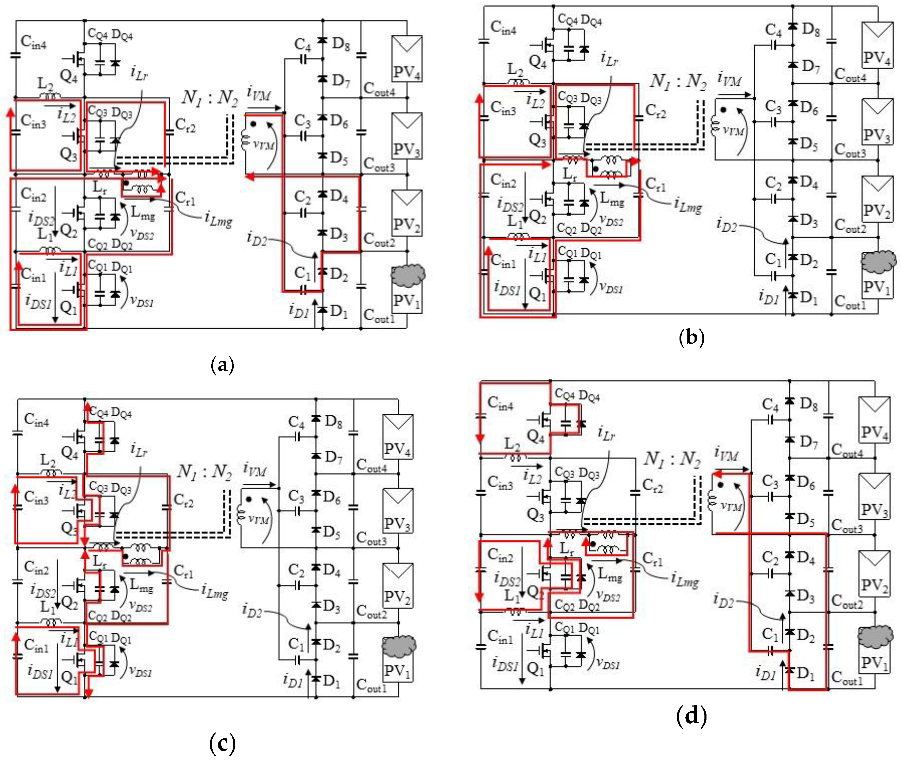
Operation modes: (a) Mode 1; (b) Mode 2; (c) Mode 3; (d) Mode 4.
Mode 1 (Figure 9a): Odd-numbered switches are on, and voltages of Q1 and Q2, vDS1 and vDS2, are zero and Vstring/2, respectively. The series connection of Cin1 and Cin2 is connected in parallel with the series connection of Cr1 and Cr2, and therefore, voltages of these series-connected capacitors become uniform. Currents of L1, L2, and Lmg (iL1, iL2, and iLmg) linearly increase as they are charged by Cin1, Cin3, and Cr2, respectively. Meanwhile, the current of Lr, iLr, sinusoidally changes due to the resonance between Lr and Cr1–Cr2. A current equal to iLr – iLmg is transferred to the secondary side in the form of iVM = N (iLr − iLmg) where N (= N1/N2) is the transformer turn ratio. C1 in the VM is charged by iVM through the diode D2. After half the resonant period, iLr becomes equal to iLmg, and the operation shifts to the next mode.
Mode 2 (Figure 9b): iLmg and iLr are equal and linearly increase. In the VD, iL1 and iL2 still linearly increase. On the secondary side, no currents flow in the VM, except for output smoothing capacitors.
Mode 3 (Figure 9c): The gating signal for Q1, vGS1 is removed to turn off Q1, and CQ1 and CQ2 start to be charged and discharged by iLmg, respectively. vDS1 increases with a slope, thus achieving ZVS turn-off. Meanwhile, vDS2 decreases with a slope equal to that of vDS1 because the sum of vDS1 and vDS2 is always equal to the total voltage of Cin1 and Cin2 (i.e., Vstring/2). This turn-off operation is essentially identical to that of traditional LLC resonant converters.
Mode 4 (Figure 9d): Charging and discharging of CQ1 and CQ2 are completed. vDS1 and vDS2 become Vstring/2 and 0, respectively, and the body diode of Q2, DQ2, starts conducting. Meanwhile, iL1, iL2, and iLmg start linearly decreasing as they are charged by Cin2, Cin4, and Cr1, respectively. Sinusoidal resonant current iLr starts flowing again due to the resonance between Lr and Cr1–Cr2. In the VM, iVM flows through the low-side diode, D1.
Mode 5: While DQ2 is conducting (i.e., vDS2 = 0), the gating signal for Q2, vGS2, is applied to turn on Q2 to achieve ZVS turn-on. This operation mode is symmetric to Mode 1.
Operations in Mode 5–8 are symmetric to those in Mode 1–4 and therefore are omitted to save page length. Since average currents of iL1 and iL2 are zero, small inductors with a small current rating can be used for L1 and L2. In the VM, currents flow through diodes and a capacitor that are connected to the shaded panel of PV1, while other diodes and capacitors are not in operation. Average current of a capacitor under steady-state conditions must be zero, and therefore, an equalization current supplied from the DPP converter to PV1 is equal to an average current of D1 or D2.
3.2. Operation Boundary
In order for Modes 2 and 3 to exist, half the resonant period must be shorter than half the switching period. To this end, the following operation condition needs to be fulfilled;
where fs, fr, and f0 are the switching frequency, higher resonant frequency, and lower resonant frequency, respectively.
3.3. Voltage Equalization Mechanism of Voltage Multiplier
The VM, shown in Figure 10, is essentially a single-input-multi-output converter that converts an input ac voltage vVM with a peak-to-peak value of Vpp into a dc voltage with a magnitude of Vpp. In Figure 10, for example, when an ac voltage vVM with Vpp = VPV is inputted, the VM produces uniform output voltages of VPV across Cout1–Cout4. C1–C4 in the VM behave as ac coupling capacitors that block dc currents and allow ac components only to flow through them. Hence, by removing dc components, the VM can be transformed to an equivalent circuit shown on the right-hand side, in which all the PV panels are separated and grounded. Since all PV panels are equivalently connected in parallel, all the voltages of panels as well as Cout1–Cout4 are automatically equalized. Detailed operation analyses have been performed in past works [28].
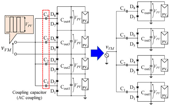
Figure 10.
VM and its equivalent circuit.
3.4. Design Guideline for LLC Resonant Inverter
In general, a ratio of Lmg to Lr for ordinary LLC resonant converters is designed to be around 5–10 in order to obtain proper gain-frequency characteristics [34]; ratios vary depending on applications but do not exceed 10 in most applications. The proposed LLC resonant VM-based DPP converter, on the other hand, operates at a fixed switching frequency with a fixed duty cycle. Since ordinary PV panels are generally installed so that partial shading does not occur as far as possible, the proposed DPP converter should be designed to minimize the loss under unshaded conditions, which correspond to no-load conditions for ordinary LLC resonant converters. A small value in Lmg leads to an increased loss due to a large iLmg under no-load conditions. Hence, to reduce the loss originating from iLmg, Lmg in the proposed DPP converter should be designed to be large within the range that iLmg can completely charge and discharge CQ of MOSFETs in order to achieve the ZVS operations.
Since the ratio of Lr to Lmg of the LLC resonant tank (approximately 150 in the prototype, see Table 1) is rather larger than that of ordinary LLC resonant converter (around 5–10), the LLC resonant tank in the proposed DPP converter operates more like a series-resonant tank. Therefore, similar to traditional series-resonant tanks, the gain of the LLC resonant tank in the proposed DPP converter is unity at the higher resonant frequency fr. It suggests the turns ratio of the transformer can be determined by assuming the unity gain of the LLC resonant tank.

Table 1.
Circuit components used for prototype.
The voltages of Cr1 and Cr2 are alternately applied to the transformer primary winding, and Vpp is equal to Vstring/2. As mentioned in Section 3.3, the voltages of the VM’s outputs (i.e., Cout1–Cout4) are equal to the peak-to-peak value of the VM’s input voltage vVM (or the voltage of the secondary winding), yielding the following equation:
where VPV is the voltage of the panel that receives an equalization current from the DPP converter. Assuming all voltages are ideally equalized to be VPV, substituting Vstring = 4VPV into (2) produces:
This equation corresponds to an ideal condition. In practical cases, however, considering forward voltage drops of diodes and voltage drops in resistive components in switches and capacitors, the turns ratio should be determined so that 2N2 is slightly larger than N1 (i.e., 2N2 > N1).
3.5. Peak Current of Inductor
Since the string voltage Vstring is divided by the VD, the voltages applied to the inductors in the VD can be reduced, contributing to reduced peak inductor currents. The peak current of the inductors, IL.peak, can be yielded as:
where VCin is the voltage of Cin1–Cin4, Ts (= 1/fs) is the switching period, and L is the inductance. Applying the experimental conditions (Vstring = 142.5 V, VCin = 35.6 V, Ts = 7.15 μs, and L = 470 μH), IL.peak is calculated to be 136 mA. Although Vstring is 142.5 V, IL.peak can be as low as 136 mA with L = 470 μH thanks to the zero average currents of the inductors.
4. Experimental Results
4.1. Prototype
Previous works reported that DPP converters capable of processing 30% of panel power are sufficient to preclude loss in annual energy yield in most cases [35,36]. As long as panels are installed in a proper location, severe shading conditions rarely occur. We assumed that two out of four panels are shaded at the same time and their short circuit currents are 30% less than those of unshaded panels in the worst shading condition. Accordingly, for a PV string consisting of four 200 W panels connected in series, each with a short-circuit current of 5.0 A and open-circuit voltage of 45 V, a prototype capable of supplying 60 W for each shaded substring was designed and built as shown in Figure 11. Component values used for the prototype are listed in Table 1. The maximum power rating of the prototype was 120 W. Except for Cr1 and Cr2, MLCCs were employed as capacitors in the prototype. The higher resonant frequency fr was 164 kHz, and the prototype was operated at fs = 140 kHz with a dead time period of 0.4 μs.
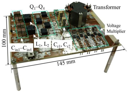
Figure 11.
Prototype capable of supplying 60 W for each shaded panel in PV string consisting of four panels connected in series.
4.2. Fundamental Characteristics of DPP Converter
Power conversion efficiencies and output characteristics of the prototype were measured using the experimental setup shown in Figure 12. The input and output ports of the prototype were separated in order to measure power conversion efficiencies and output characteristics. All PV panels were removed, and the prototype was powered by an external power supply Vin. A variable resistor Rvar was connected to the output of the VM through the selective tap to emulate current flow paths under partial shading conditions. Selecting tap X, for example, can emulate the current flow paths under the case that PV1 is partially shaded. With the tap Y selected, the prototype behaves as if PV1 and PV2 are uniformly shaded. Vin was set to be 142.5 V, which corresponded to an MPP voltage of the string used for the experiment.
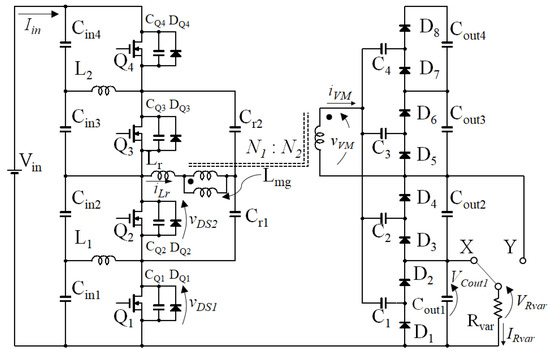
Figure 12.
Experimental setup for characteristic measurement.
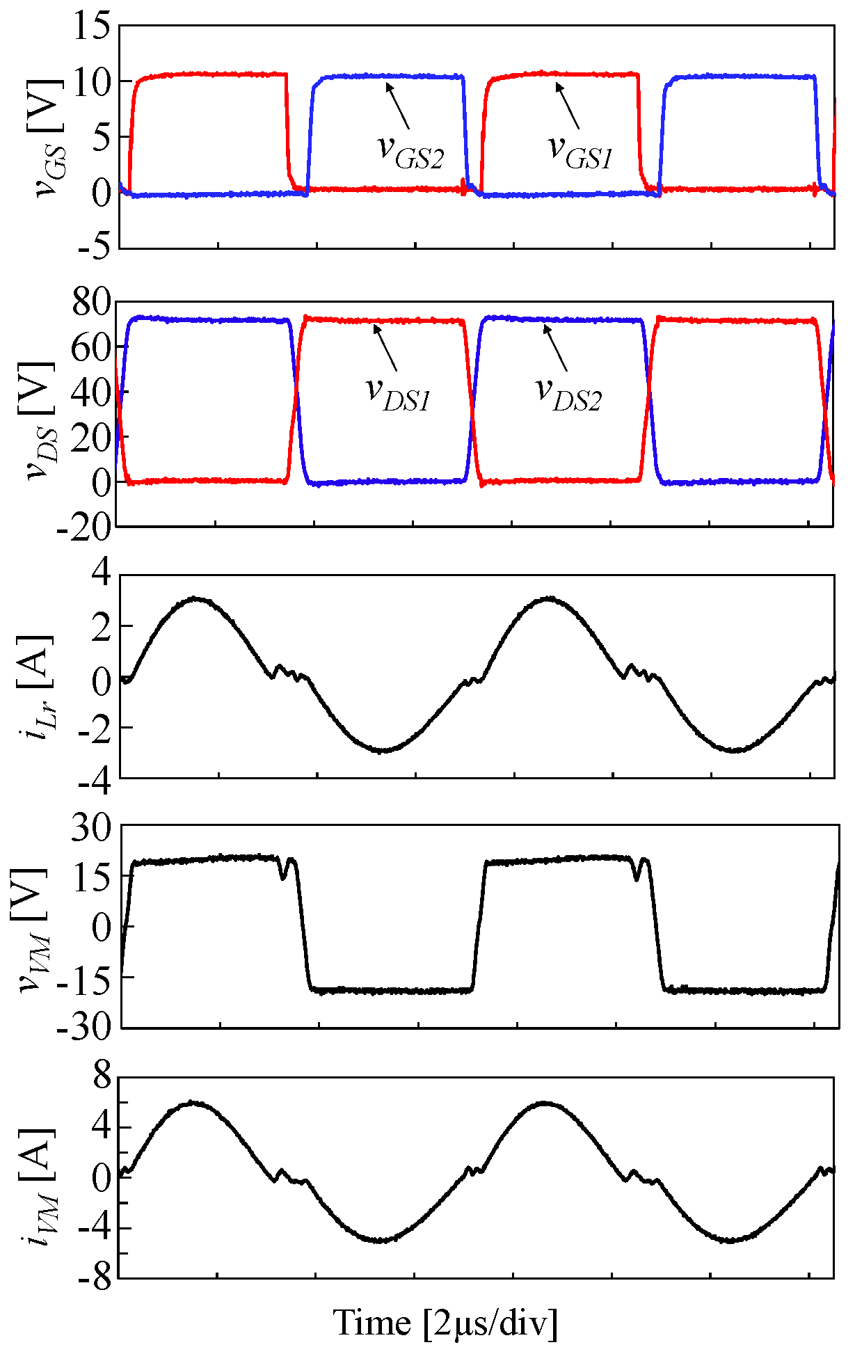
Measured key operation waveforms at IRvar = 1.5 A with the tap X selected are shown in Figure 13. Peak voltages of vDS1 and vDS2 were about 71.3 V, nearly half the input voltage Vin of 142.5 V, demonstrating that the input voltage was properly divided by the VD. Measured waveforms of vGS1, vGS2, vDS1, and vDS2 were in good agreement with theoretical ones (see Figure 8), demonstrating ZVS turn-on and turn-off operations.
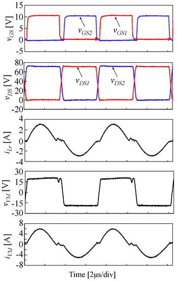
Figure 13.
Measured key operation waveforms at IRvar = 1.5 A with tap X selected.
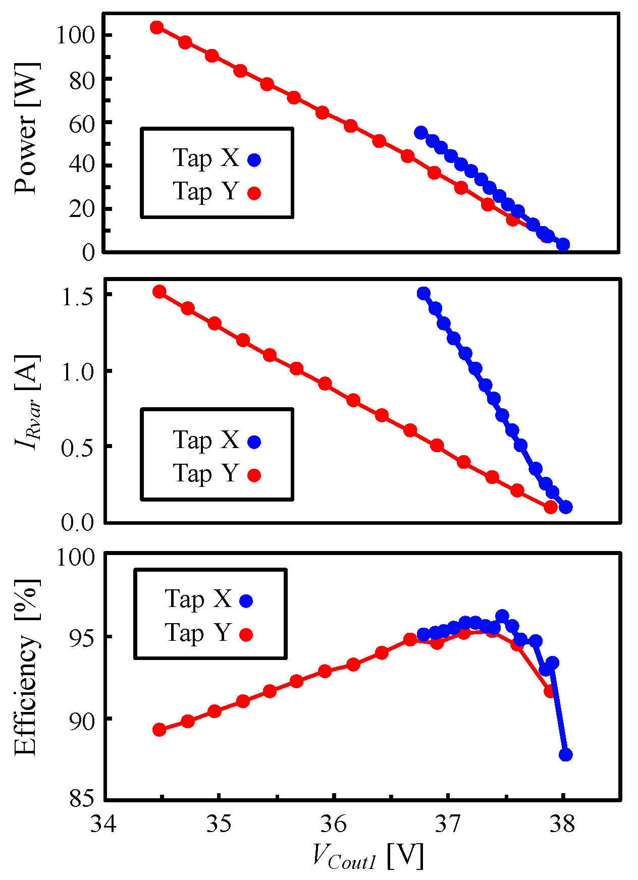
Measured power conversion efficiencies and output characteristics are shown in Figure 14. VCout1 on the horizontal axis corresponds to the voltage of Cout1 or the voltage of the shaded panel in the practical case. Voltages of Cout1–Cout4 were nearly uniform thanks to the voltage equalization performance of the VM. The measured efficiencies were mostly higher than 90%. VCout1 linearly declined as IRvar increased, and this tendency was more explicit when the tap Y was selected. It was because, with the tap Y selected, the input current of the prototype was twice that with the tap X selected, causing larger voltage drops in the VD on the transformer primary side.

Figure 14.
Measured power conversion efficiencies and output characteristics.
4.3. Equalization Test in Laboratory
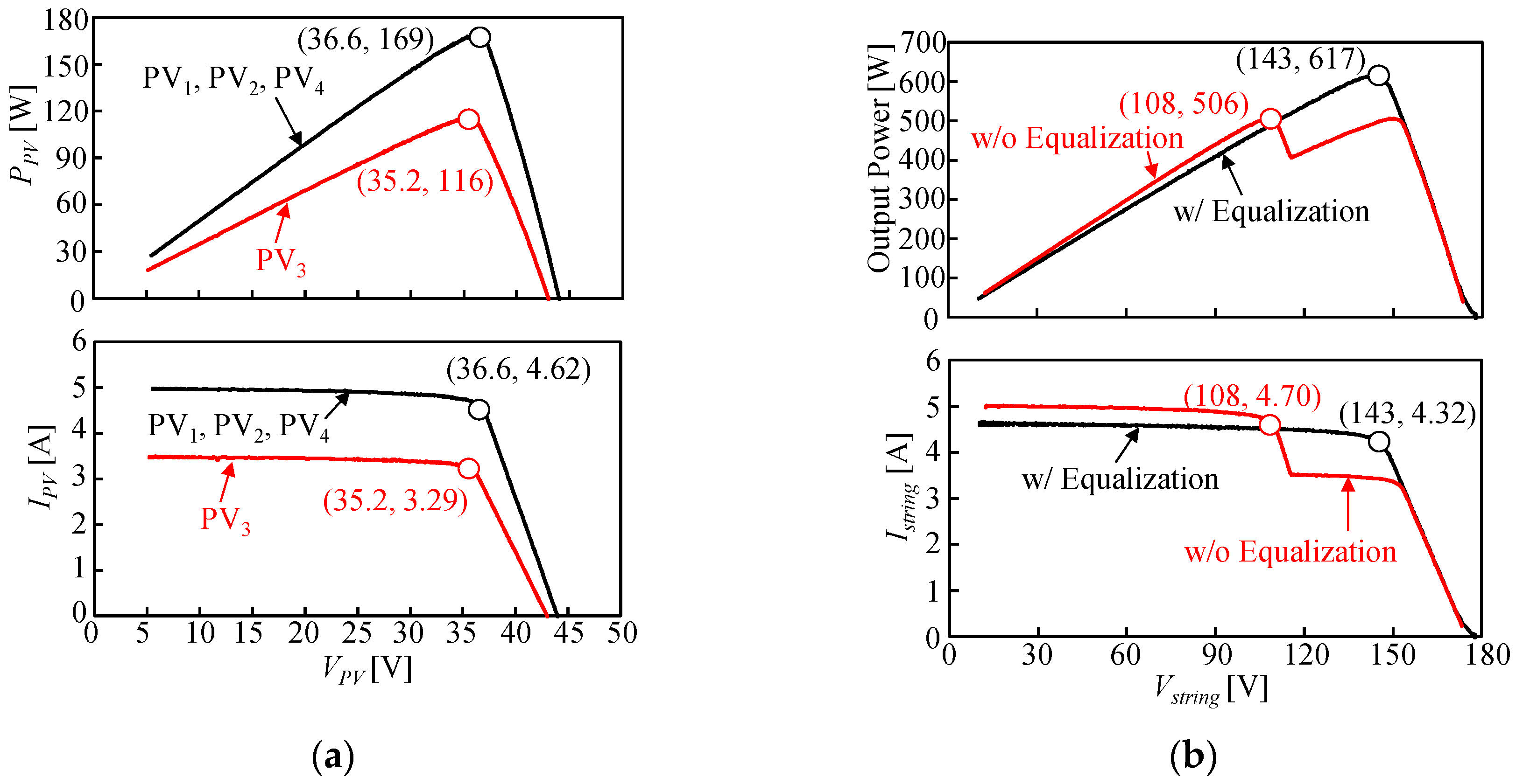
Instead of actual PV panels, solar array simulators (E4361A, Keysight Technologies) were used to emulate a partial shading condition. Individual panel characteristics used for the laboratory experiment are shown in Figure 15a. PV3 was a partially shaded panel, and its short-circuit current was 30% less than the others. The ideal maximum power of the string under this partial shading condition was 623 W. An electronic load was connected to the load port (see the port denoted as Load+ and Load− in Figure 5a) in order to sweep the string characteristics. A string characteristic without the DPP converter (i.e., with traditional bypass diodes) was also measured as a reference.
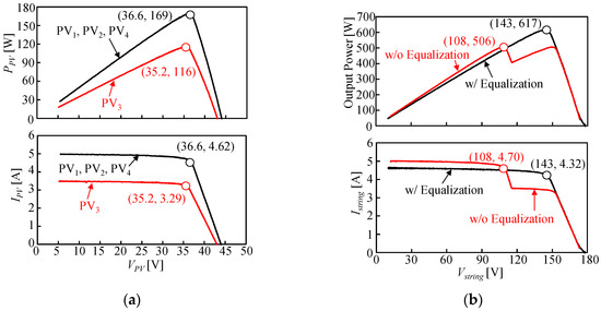
Figure 15.
Experimental results of laboratory testing. (a) Individual panel characteristics used for experiment; (b) Measured string characteristics with/without proposed DPP converter.
Measured string characteristics with/without the proposed DPP converter are compared in Figure 15b. Two MPPs, including a local and global MPPs, were observed on the P–V characteristic in the case without the DPP converter (i.e., with bypass diodes), and the maximum power was 506 W at Vstring = 108 V. With the DPP converter, on the other hand, the local MPP disappeared, and the maximum power increased to as high as 617 W at Vstring = 143 V, corresponding to 21.9%. The overall efficiency, which is defined as the ratio of the extracted power to the ideal maximum power, was determined to be 99.0% (= 617/623). The proposed DPP converter successfully increased the energy yield and demonstrated its efficacy.
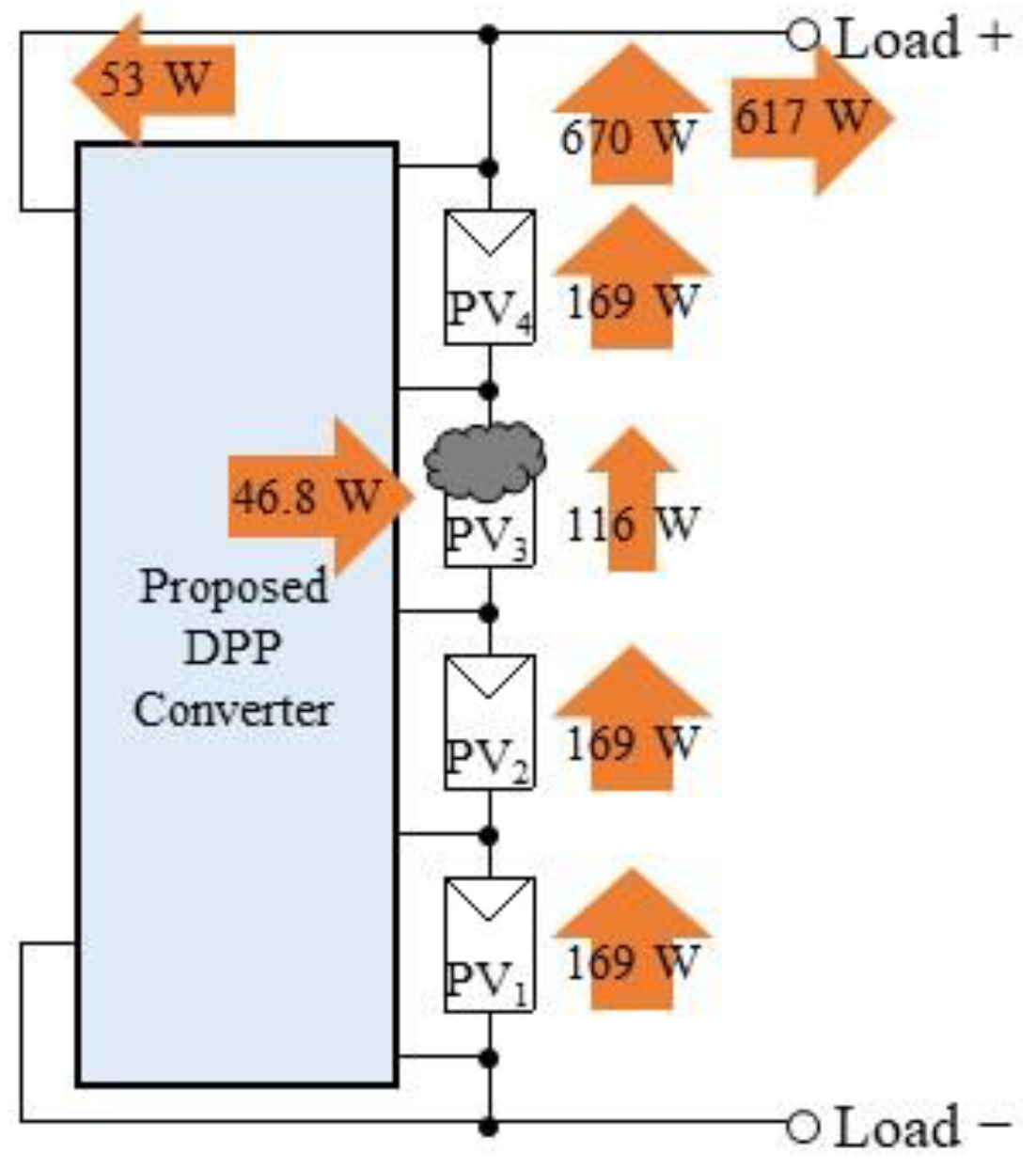
An image of power redistribution in laboratory testing is illustrated in Figure 16. Assume all the panel voltages were uniform as 35.2 V. Since the current mismatch between the shaded and unshaded panels was 1.33 A, the DPP converter supplied 46.8 W to the shaded panel of PV3 for equalization. Due to the support by the DPP converter, the string behaved as if it produced 670 W. However, since 53 W out of 670 W was inputted to the DPP converter, the extracted power at the load port was 617 W. The power processed by the DPP converter under this partial shading condition was merely 53 W and was rather smaller than the string power. This small processed power allowed the 99% overall efficiency, even though the measured efficiency of the DPP converter was around 90% (see Figure 14).

Figure 16.
Power redistribution image in laboratory testing.
4.4. Field Testing
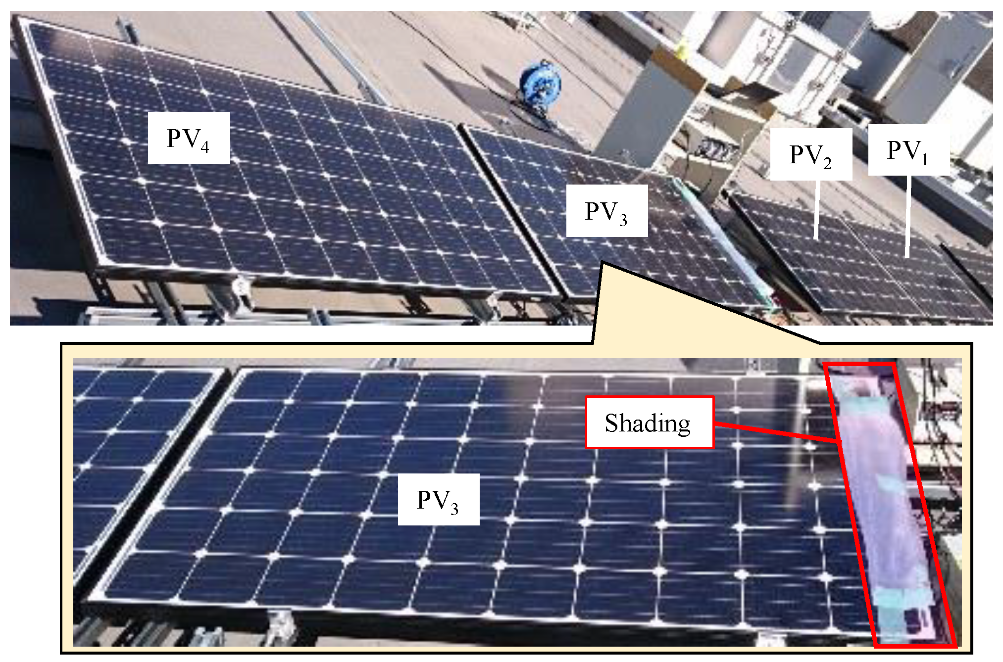
Field testing using an actual string consisting of four PV panels connected in series was performed, as shown in Figure 17. PV3 was covered with a plastic bag to emulate the partial shading condition. Measured individual panel characteristics are shown in Figure 18a. The irradiance was measured to be 591 W/m2 by a pyranometer (ES-602, EKO). The short-circuit current of PV3 was 16.7% less than the others. The ideal maximum power under this shading condition was 672 W. Similar to the laboratory testing, string characteristics with/without the DPP converter were swept using the electronic load.
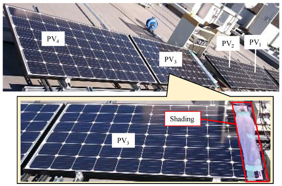
Figure 17.
Experimental setup for field testing.
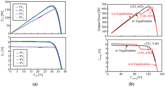
Figure 18.
Experimental results of field testing. (a) Individual panel characteristics used for experiment; (b) Measured string characteristics with/without proposed DPP converter.
Measured string characteristics are shown in Figure 18b. The string characteristic without the DPP converter (i.e., with traditional bypass diodes) exhibited two MPPs, and the maximum power at the global MPP was 625 W at Vstring = 130 V. With the DPP converter, the local MPP vanished, and the maximum power increased to 652 W at Vstring = 121 V, corresponding to the overall efficiency of 97.0% (= 652/672). These results demonstrate the improved energy yield of the actual PV string.
4.5. Extended DPP Converter for Eight Panels Connected in Series
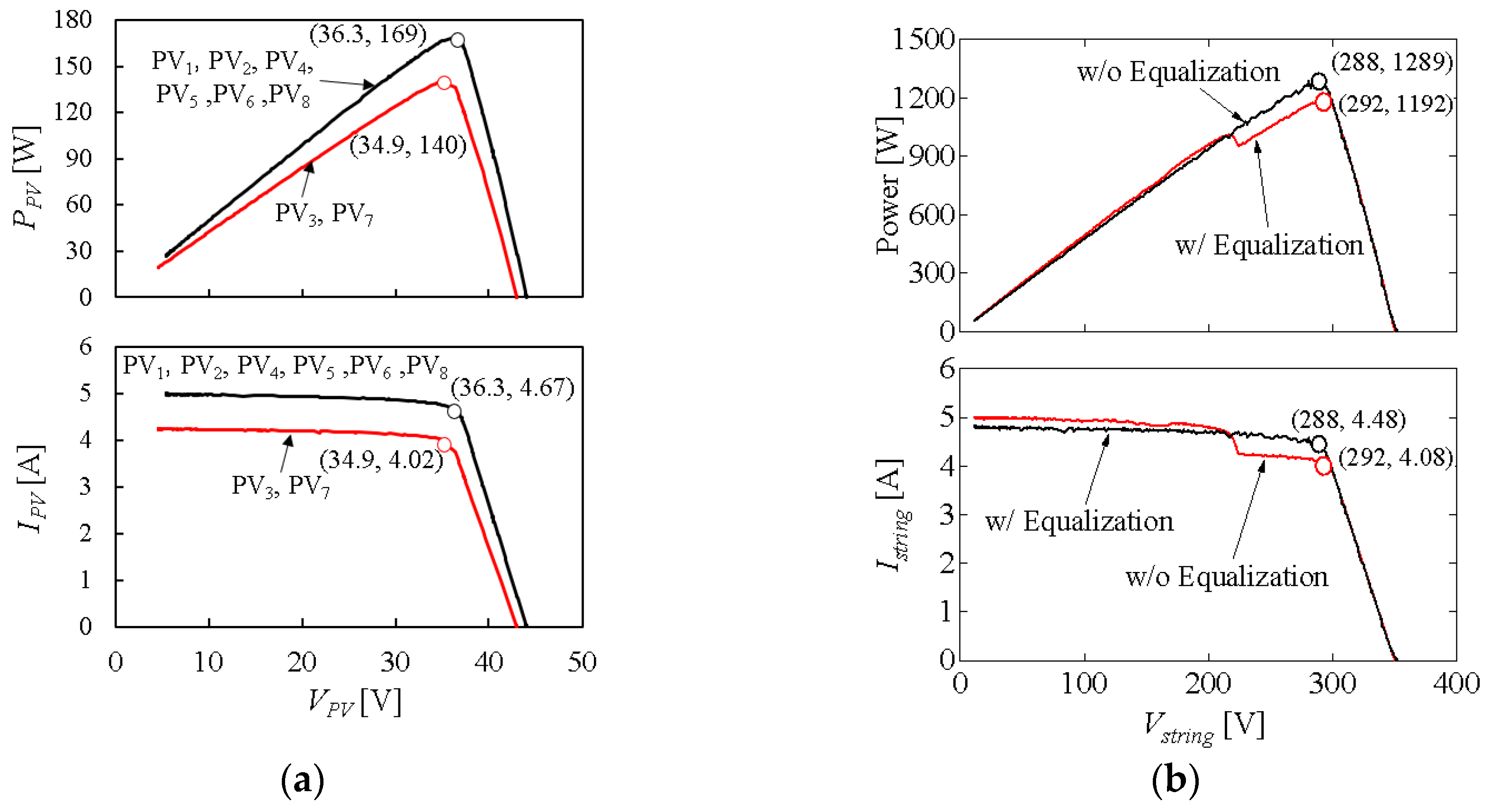
A prototype of the extended topology for eight panels connected in series was also built and tested. Although the extended topology consists of more circuit components, component values used for the prototype were identical to those shown in Table 1. An equalization test was performed in the laboratory using the solar array simulators. Individual panel characteristics used for the experiment are shown in Figure 19a. PV3 and PV7 were shaded panels, and their short-circuit current was 15% less than the others. The ideal maximum power of the string was 1294 W.
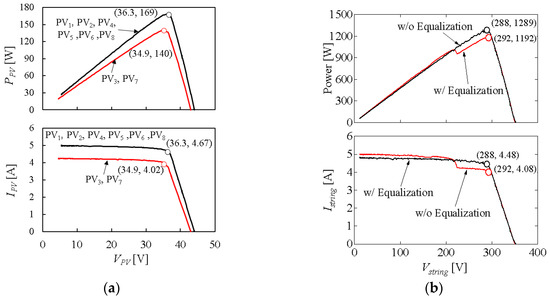
Figure 19.
Experimental results of extended DPP converter. (a) Individual panel characteristics used for experiment; (b) Measured string characteristics with/without proposed DPP converter.
Measured string characteristics with/without the DPP converter are compared in Figure 19b. Two MPPs were observed when without the DPP converter, and the maximum power at the global MPP was 1192 W at Vstring = 292 V. With the DPP converter, on the other hand, the local MPP vanished, and the maximum power increased to 1289 W at Vstring = 288 V, corresponding to 8.2% improvement. The overall efficiency was as high as 99.6% (=1289/1294). The results demonstrated the extension concept of the proposed DPP converter.
5. Conclusions
This paper has proposed a DPP converter using an LLC resonant VM and VD. Voltage stresses of circuit components in conventional string-to-panel DPP converters are prone to soar as the string voltage increases. Meanwhile, the proposed DPP converter can reduce voltage stresses of switches and input smoothing capacitors thanks to the VD. The proposed DPP converter can automatically transfer power from unshaded panels to shaded ones, and therefore a feedback control loop can be eliminated, achieving simplified circuit implementation. The VD can be extended by adding switches and capacitors, and the voltage stresses can be further reduced by extending the VD.
Experimental verification tests using the prototype for four PV panels connected in series were performed emulating partial shading conditions in the laboratory and outdoor testing. The proposed DPP converter dramatically improved the energy yield and achieved the overall efficiency higher than 97%, demonstrating its performance. Furthermore, the prototype of the extended topology for eight panels connected in series was also built and tested, and its experimental results demonstrated the extension concept of the proposed DPP converter.
Author Contributions
Conceptualization, M.U.; methodology, M.U.; simulation analysis, T.N. and T.S.; validation, T.N.; writing—original draft preparation, M.U. and T.N.; writing—review and editing, M.U. and T.S.; supervision, M.U.
Funding
This research received no external funding.
Conflicts of Interest
The authors declare no conflict of interest.
References
- MacAlpine, S.M.; Erickson, R.W.; Brandemuehl, M.J. Characterization of power optimizer potential to increase energy capture in photovoltaic systems operating under nonuniform conditions. IEEE Trans. Power Electron. 2013, 28, 2936–2945. [Google Scholar] [CrossRef]
- Ramli, M.A.M.; Twaha, S.; Ishaque, K.; Turki, Y.A.A. A review on maximum power point tracking for photovoltaic systems with and without shading conditions. Renew. Sustain. Energy Rev. 2017, 67, 144–159. [Google Scholar] [CrossRef]
- Qin, S.; Cady, S.T.; García, A.D.D.; Podgurski, R.C.N.P. A distributed approach to maximum power point tracking for photovoltaic submodule differential power processing. IEEE Trans. Power Electron. 2015, 30, 2024–2040. [Google Scholar] [CrossRef]
- Qin, S.; Barth, C.B.; Podgurski, R.C.N.P. Enhancing microinverter energy capture with submodule differential power processing. IEEE Trans. Power Electron. 2016, 31, 3575–3585. [Google Scholar] [CrossRef]
- Bergveld, H.J.; Büthker, D.; Castello, C.; Doorn, T.; Jong, A.D.; Otten, R.V.; Waal, K.D. Module-level dc/dc conversion for photovoltaic systems: The delta-conversion concept. IEEE Trans. Power Electron. 2013, 28, 2005–2013. [Google Scholar] [CrossRef]
- Shenoy, P.S.; Kim, K.A.; Johnson, B.B.; Krein, P.T. Differential power processing for increased energy production and reliability of photovoltaic systems. IEEE Trans. Ind. Power Electron. 2013, 28, 2968–2979. [Google Scholar] [CrossRef]
- Shimizu, T.; Hirakata, M.; Kamezawa, T.; Watanabe, H. Generation control circuit for photovoltaic modules. IEEE Trans. Power Electron. 2001, 16, 293–300. [Google Scholar] [CrossRef]
- Shimizu, T.; Hashimoto, O.; Kimura, G. A novel high-performance utility-interactive photovoltaic inverter system. IEEE Trans. Power Electron. 2003, 18, 704–711. [Google Scholar] [CrossRef]
- Wang, F.; Zhu, T.; Zhuo, F.; Yi, H. An improved submodule differential power processing-based PV system with flexible multi-MPPT control. IEEE J. Emerg. Sel. Top. 2018, 6, 94–102. [Google Scholar] [CrossRef]
- Ramli, M.Z.; Salam, Z. A simple energy recovery scheme to harvest the energy from shaded photovoltaic modules during partial shading. IEEE Tran. Power Electron. 2014, 29, 6458–6471. [Google Scholar] [CrossRef]
- Blumenfeld, A.; Cervera, A.; Peretz, M.M. Enhanced differential power processor for PV systems: Resonant switched-capacitor gyrator converter with local MPPT. IEEE J. Emerg. Sel. Top. Power Electron. 2014, 2, 883–892. [Google Scholar] [CrossRef]
- Gokdaga, M.; Akbabab, M.; Gulbudakc, O. Switched-capacitor converter for PV modules under partial shading and mismatch conditions. Sol. Energy 2018, 170, 723–731. [Google Scholar] [CrossRef]
- Uno, M.; Kukita, A. PWM converter integrating switched capacitor converter and series-resonant voltage multiplier as equalizers for photovoltaic modules and series-connected energy storage cells for exploration rovers. IEEE Trans. Power Electron. 2017, 32, 8500–8513. [Google Scholar] [CrossRef]
- Stauth, J.T.; Seeman, M.D.; Kesarwani, K. Resonant switched-capacitor converters for sub-module distributed photovoltaic power management. IEEE Trans. Power Electron. 2013, 28, 1189–1198. [Google Scholar] [CrossRef]
- Chang, A.H.; Avestruz, A.T.; Leeb, S.B. Capacitor-less photovoltaic cell-level power balancing using diffusion charge redistribution. IEEE Trans. Power Electron. 2015, 30, 537–546. [Google Scholar] [CrossRef]
- Uno, M.; Saito, Y.; Yamamoto, M.; Urabe, S. PWM switched capacitor-based cell-level power balancing converter utilizing diffusion capacitance of photovoltaic cells. IEEE Trans. Power Electron. 2019, 34, 10675–10687. [Google Scholar] [CrossRef]
- Uno, M.; Yamamoto, M.; Sato, H.; Oyama, S. Modularized differential power processing architecture based on switched capacitor converter to virtually unify mismatched photovoltaic panel characteristics. IEEE Trans. Power Electron. 2019, in press. [Google Scholar] [CrossRef]
- Olalla, C.; Clement, D.; Rodríguez, M.; Makisimović, D. Architectures and control of submodule integrated dc-dc converters for photovoltaic applications. IEEE Trans. Power Electron. 2013, 28, 2980–2997. [Google Scholar] [CrossRef]
- Levron, Y.; Clement, D.R.; Choi, B.; Olalla, C.; Maksimovic, D. Control of submodule integrated converters in the isolated-port differential power-processing photovoltaic architecture. IEEE J. Emerg. Sel. Top. Power Electron. 2014, 2, 821–832. [Google Scholar] [CrossRef]
- Bell, R.; Podgurski, R.C.N.P. Decoupled and distributed maximum power point tracking of series-connected photovoltaic submodules using differential power processing. IEEE J. Emerg. Sel. Top. Power Electron. 2015, 3, 881–891. [Google Scholar] [CrossRef]
- Olalla, C.; Deline, C.; Clement, D.; Levron, Y.; Rodríguez, M.; Makisimović, D. Performance of power limited differential power processing architectures in mismatched PV systems. IEEE Trans. Power Electron. 2015, 30, 618–631. [Google Scholar] [CrossRef]
- Chu, G.; Wen, H.; Jiang, L.; Hu, Y.; Li, X. Bidirectional flyback based isolated-port submodule differential power processing optimizer for photovoltaic applications. Sol. Energy 2017, 158, 929–940. [Google Scholar] [CrossRef]
- Jeon, Y.T.; Lee, H.; Kim, K.A.; Park, J.H. Least power point tracking method for photovoltaic differential power processing systems. IEEE Trans. Power Electron. 2017, 32, 1941–1951. [Google Scholar] [CrossRef]
- Jeon, Y.T.; Park, J.H. Unit-minimum least power point tracking for the optimization of photovoltaic differential power processing systems. IEEE Trans. Power Electron. 2019, 34, 311–324. [Google Scholar] [CrossRef]
- Du, J.; Xu, R.; Chen, X.; Li, Y.; Wu, J. A novel solar panel optimizer with self-compensation for partial shadow condition. In Proceedings of the IEEE Applied Power Electron. Conference and Exposition (APEC), Long Beach, CA, USA, 17–21 March 2013; pp. 92–96. [Google Scholar]
- Uno, M.; Kukita, A. Single-switch voltage equalizer using multi-stacked buck–boost converters for partially-shaded photovoltaic modules. IEEE Trans. Power Electron. 2015, 30, 3091–3105. [Google Scholar] [CrossRef]
- Uno, M.; Kukita, A. Current sensorless equalization strategy for a single-switch voltage equalizer using multistacked buck–boost converters for photovoltaic modules under partial shading. IEEE Trans. Ind. Appl. 2017, 53, 420–429. [Google Scholar] [CrossRef]
- Uno, M.; Kukita, A. Two-switch voltage equalizer using an LLC resonant inverter and voltage multiplier for partially shaded series connected photovoltaics modules. IEEE Trans. Ind. Appl. 2015, 51, 1587–1601. [Google Scholar] [CrossRef]
- Uno, M.; Kukita, A. Single-switch single-magnetic PWM converter integrating voltage equalizer for partially-shaded photovoltaic modules in standalone applications. IEEE Trans. Power Electron. 2018, 33, 1259–1270. [Google Scholar] [CrossRef]
- Uno, M.; Shinohara, T. Variable switching frequency modulation scheme for PWM converter integrating series-resonant voltage multiplier-based voltage equalizer for photovoltaic strings under partial shading. IEEJ Trans. Electr. Electron. Eng. 2019, 14, 467–474. [Google Scholar] [CrossRef]
- Uno, M.; Shinohara, T.; Saito, Y.; Kukita, A. Review, comparison, and proposal for PWM converters integrating differential power processing converter for small exploration rovers. Energies 2019, 12, 1919. [Google Scholar] [CrossRef]
- Ruan, X.; Li, B.; Chen, Q.; Tan, S.C.; Tse, C.K. Fundamental considerations of three-level DC–DC converters: Topologies, analyses, and control. IEEE Trans. Power Electron. 2008, 55, 3733–3743. [Google Scholar]
- Lee, I.O.; Moon, G.W. Analysis and design of a three-level LLC series resonant converter for high- and wide-input-voltage applications. IEEE Trans. Power Electron. 2012, 27, 2966–2979. [Google Scholar] [CrossRef]
- Choi, H. Design Consideration for an LLC-Resonant Converter. Proceedings of the Fairchild Power Seminar. 2007, pp. A1–A9. Available online: http://citeseerx.ist.psu.edu/viewdoc/download?doi=10.1.1.397.2440&rep=rep1&type=pdf (accessed on 19 October 2019).
- Kim, K.A.; Shenoy, P.S.; Krein, P.T. Converter rating analysis for photovoltaic differential power processing systems. IEEE Trans. Ind. Electron. 2015, 30, 1987–1997. [Google Scholar] [CrossRef]
- Olalla, C.; Hasan, M.N.; Deline, C.; Maksimovi, D. Mitigation of hot-spots in photovoltaic systems using distributed power electronics. Energies 2018, 11, 726. [Google Scholar] [CrossRef]
© 2019 by the authors. Licensee MDPI, Basel, Switzerland. This article is an open access article distributed under the terms and conditions of the Creative Commons Attribution (CC BY) license (http://creativecommons.org/licenses/by/4.0/).

