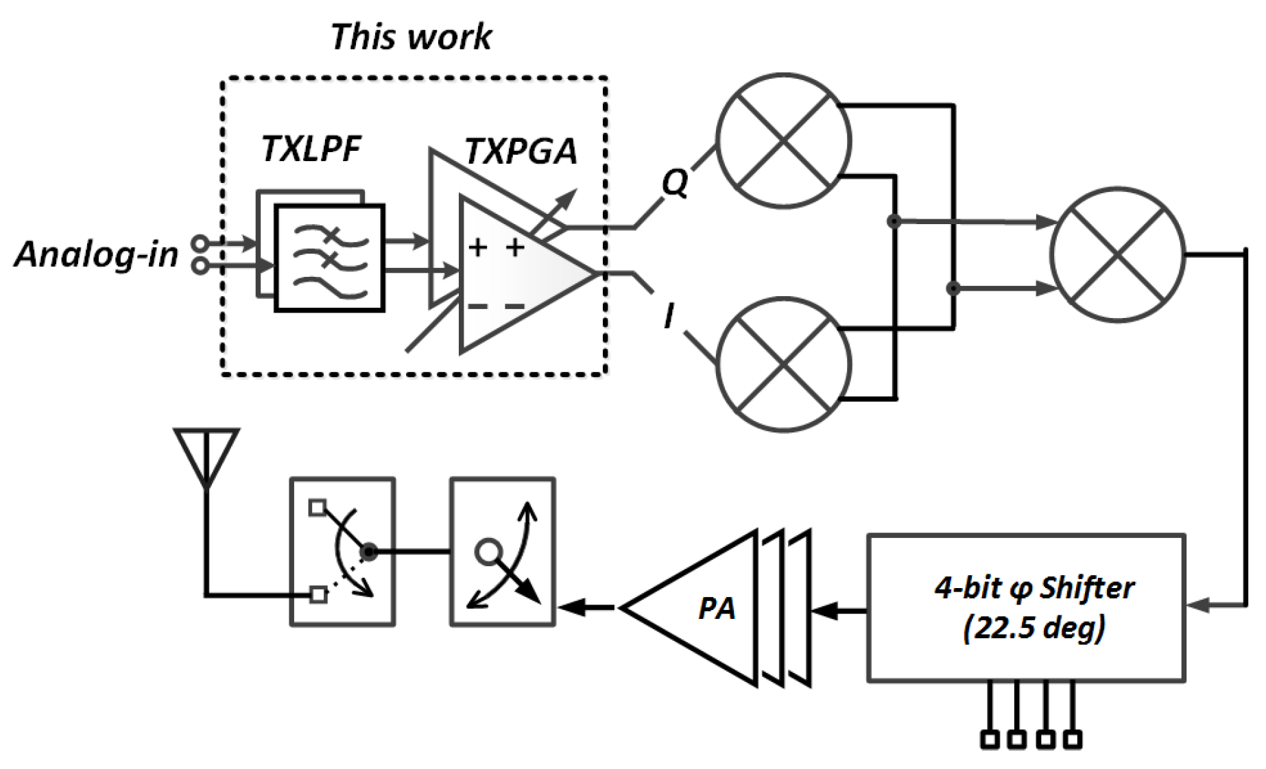
2.1. Low-Pass-Filter (LPF)
Because of the characteristics of high input resistance and low output resistance, source followers are often used as buffers. In fact, they can be simply modified into continuous-time filters by synthesizing complex poles with the feedback and capacitors [
3]. A super source follower is an improved version of the source follower. By adding an additional MOSFET to form a feedback loop, the output impedance can be reduced by a factor of the loop gain [
4]. In this work, a super source follower based low-pass-filter is implemented.
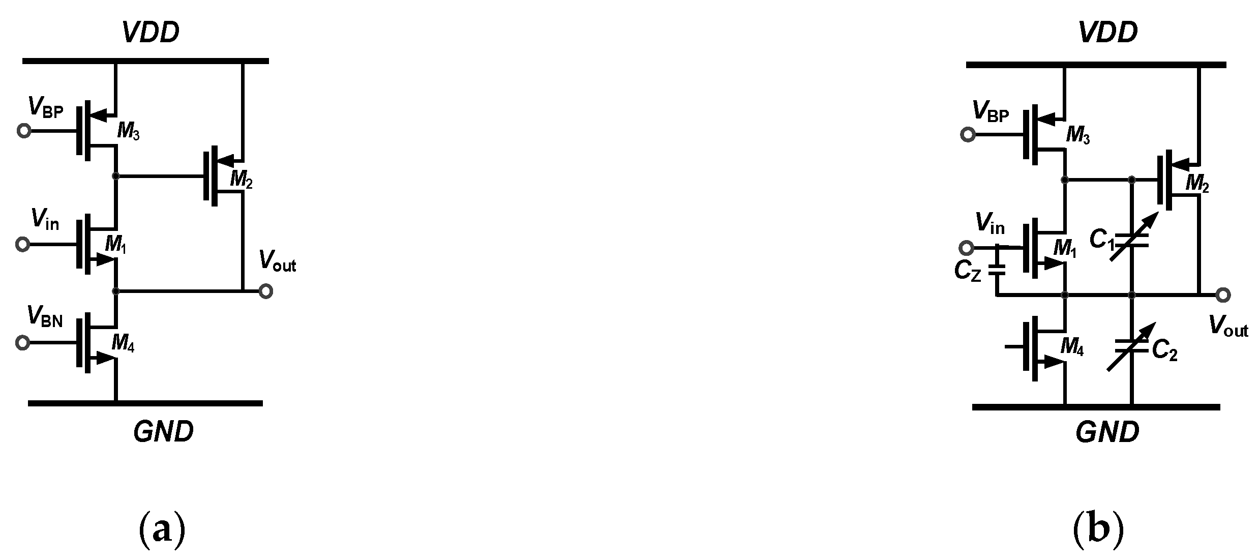
Figure 2a shows the schematic of a super-source-follower (SSF). The super source follower contains an additional local feedback formed by the transistor M
2. Transistors M
3 and M
4 are current sources. The output resistance of the SSF can be analyzed as follows. The input voltage is kept constant and let us assume that the output now experiences a voltage drop. The voltage drop not only raises the drain current of M
1 but also lowers the gate voltage of M
2. Hence, the drain current of M
2 would be increased. The output resistance is therefore reduced because of this incremental current flow through the output node. The output resistance of an SSF can be expressed as:
Notably, the output resistance of SSF is lower by a factor of
gm2ro3, as compared with that of a conventional source follower. The dc voltage gain A
0, is given in Equation (2), where the output resistance
ro of each transistor is considered:
The resistor ro24 represents the equivalent resistance of resistors ro2 and ro4 in parallel. With the reduced output resistance and improved gain, the SSF shows better driving capability, as compared to the traditional source follower.
The SSF is modified into a biquadratic low-pass filter, as shown in
Figure 2b, where capacitors
C1 and
C2 are employed to synthesis poles. In parallel with the main signal path, the gate-source capacitance of M
1 (
Cgs1) is naturally associated with a high frequency zero. Since the LPF requires a transmission zero at 2.2 GHz, a capacitor
CZ is included to move the transmission zero to the desired frequency. The transfer function of the SSF-based biquadratic filter is expressed in (3):
From the formula (3), the complex pole
ω0, the quality factor Q and the transmission zero
ωz can be obtained, as expressed in (4), (5), and (6) respectively:
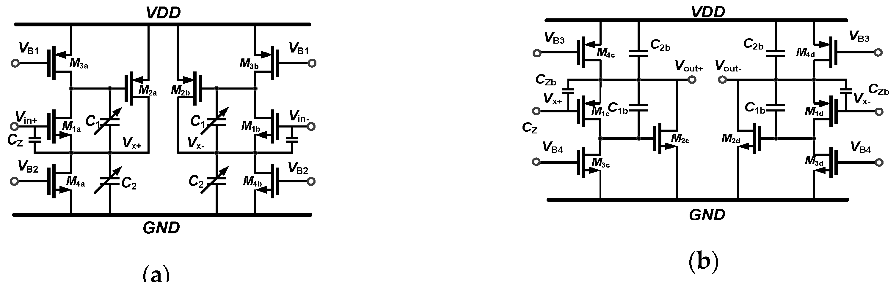
In this work, a fourth-order Elliptic LPF is designed to provide anti-aliasing function for 5G mobile communication. The fourth-order LPF is formed from two SSF biquadratic low-pass filters in cascade, as shown in
Figure 3, where the two filters use different types of input transistors so that the level shifting effect is compensated to obtain identical input and output common mode voltages [
4]. At the initial stage of design, the software “Filter Solutions” is used to determine the key parameters for the fourth-order Elliptic LPF. According to the calculation results of “Filter Solutions”, the cut-off frequency, transmission zero, and quality factor of the first biquadratic low-pass filter are set to 707 MHz, 2.2 GHz, and 0.73, respectively, while the cut-off frequency, transmission, and quality factor of the second biquadratic low-pass filter are set to 1.13 GHz, 5.27 GHz, and 3.45, respectively. Since small capacitors are used to synthesize high-frequency poles and zeroes, the LPF is very susceptible to parasitic capacitances. In order to achieve the desired frequency response, the capacitors
C1,
C2, and
CZ in the biquadratic low-pass filter are chosen by considering all the inevitable parasitic capacitances in the circuit. Moreover, the capacitors
C1 and
C2 are realized with 2-bit programmable capacitors in the first biquadratic low-pass filter so that the corner frequency and transmission zero of the LPF can be tuned to cope with process-voltage-temperature variations.
2.2. Programmable Gain Amplifier (PGA)
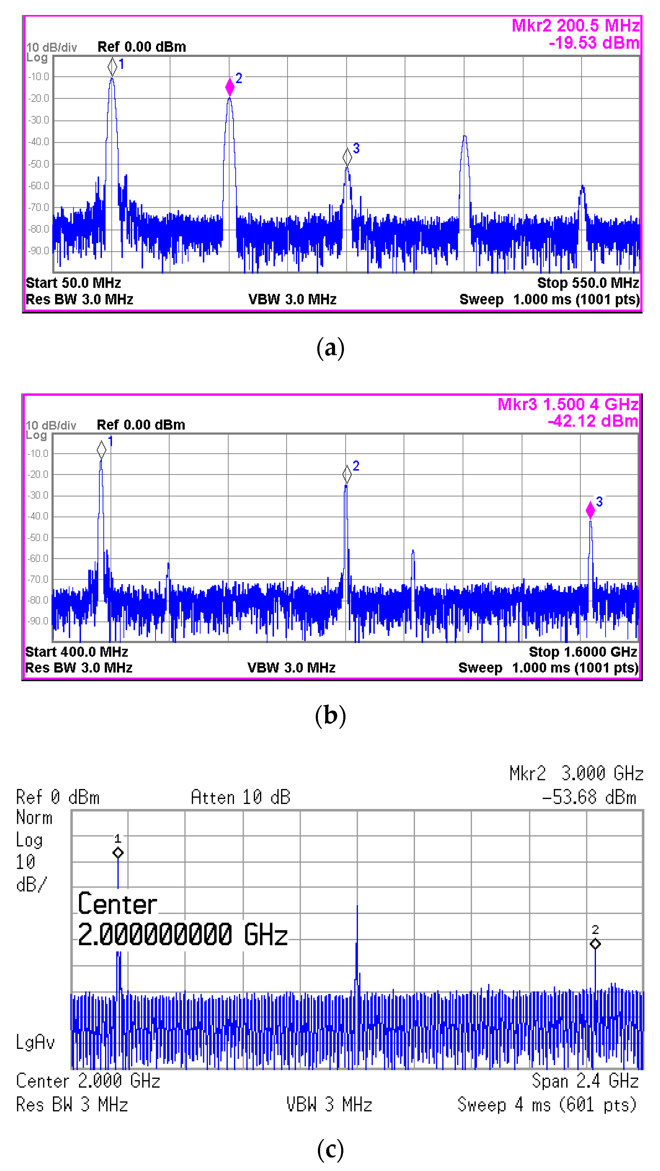
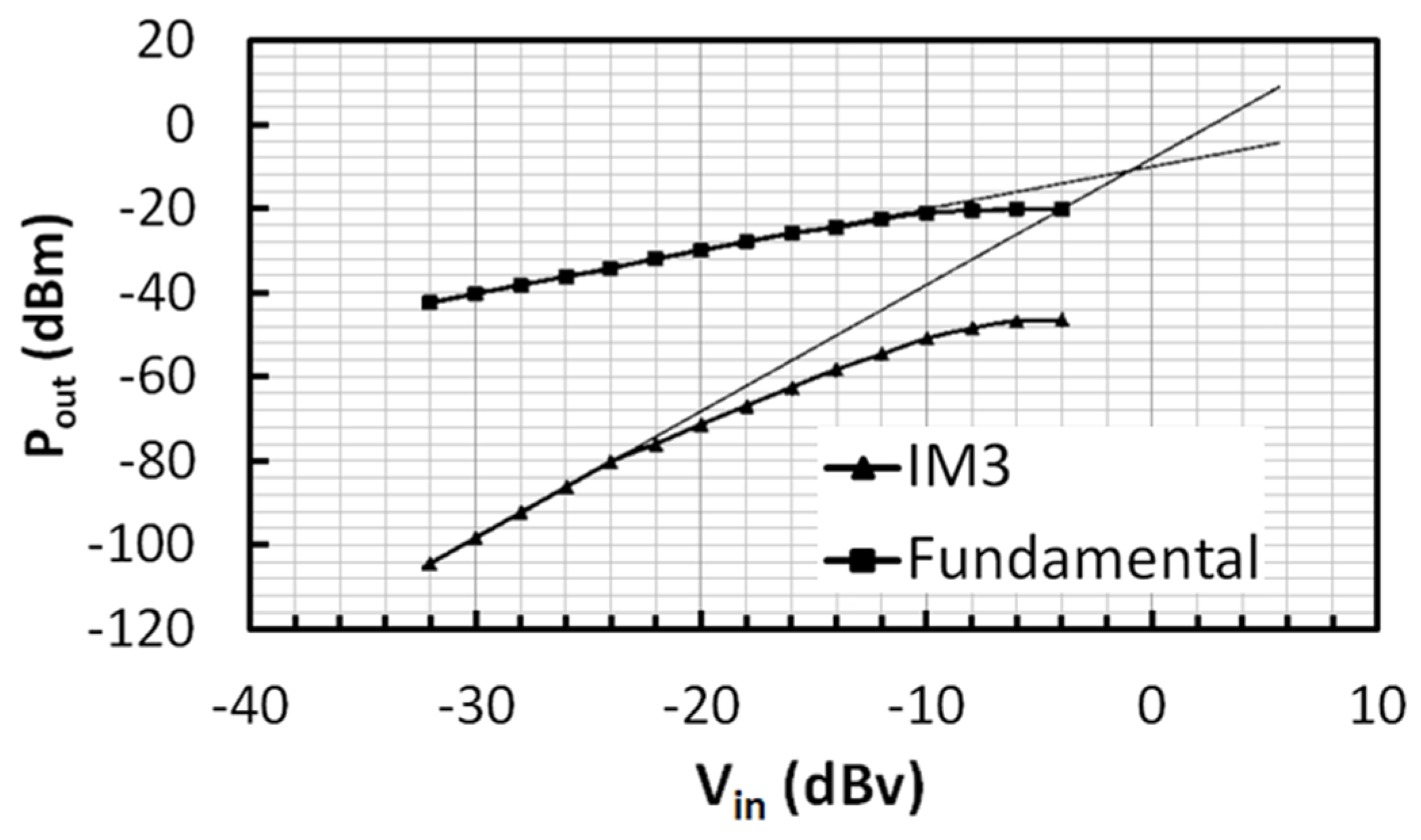
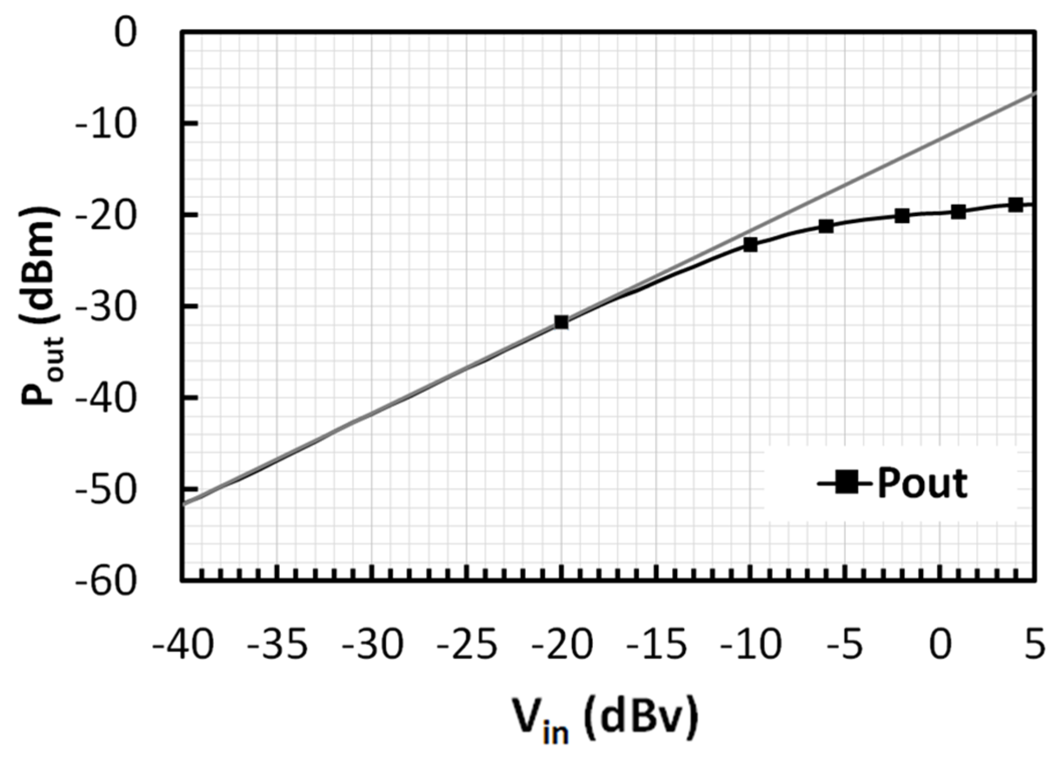
Unwanted spurs appearing in the output spectrum of an up-conversion mixer can cause serious spectrum regrowth. Since their levels are closely related to the input level of the mixer, it is necessary for the PGA to pass the mixer with a specified signal level so that these spurs can be down by 40–50 dBc. According to the simulation results of the up-conversion mixer, the desired input level of the mixer is 200 mVpp. Therefore, the PGA is designed to maintain the output level of 200 mVpp for an input dynamic range of 20 dB. With the programmable voltage gain from −16 dB to 4 dB, the PGA can handle the input level from 1.26 Vpp to 126 mVpp.
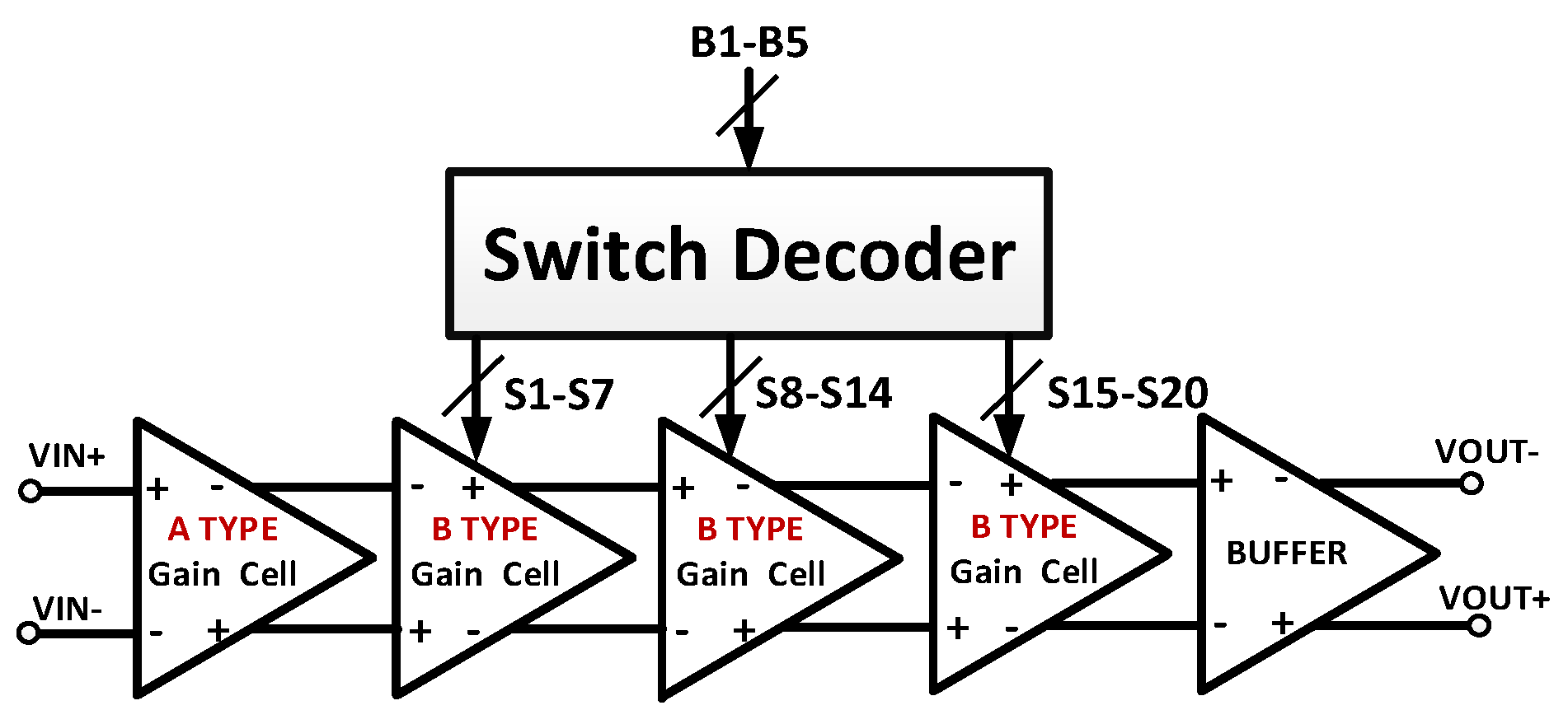
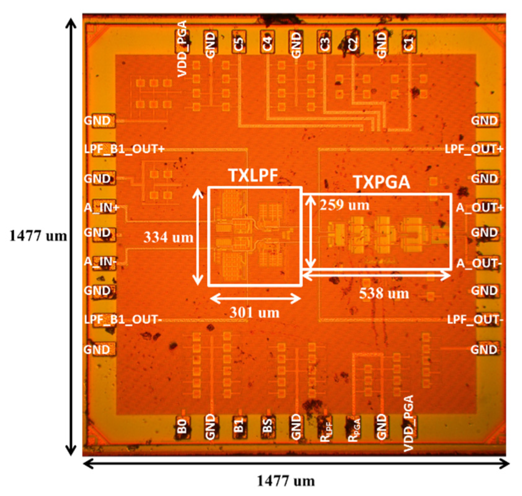
An open-loop-configured PGA is designed and implemented to achieve the required gain range. The block diagram of the programmable gain amplifier is shown in
Figure 4. Considering the tradeoff between the power consumption and bandwidth, four gain cells are connected in cascade to achieve the desired gain range. The 5-bit binary control word B
1–B
5 is translated into the 20-bit thermometer code S
1–S
20 by a switch decoder, as shown in
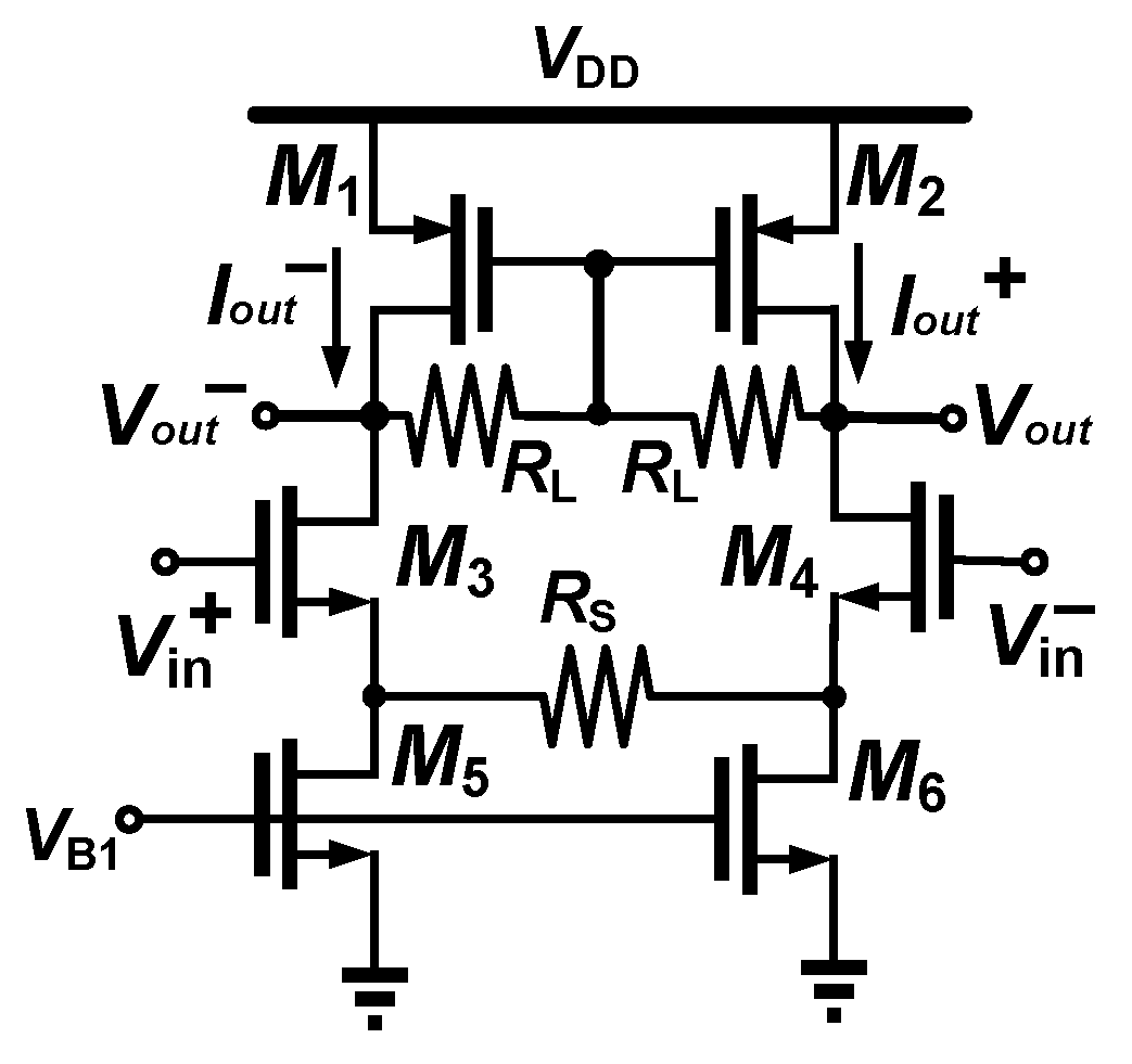
Figure 4. The first gain cell (A-type gain cell) of the PGA is a common-source amplifier with resistive source degeneration (
Figure 5). This gain cell provides the gain of −16 dB so that large baseband signals can be attenuated in the first stage. In this way, the linearity requirement of the rest gain cells can be relaxed.
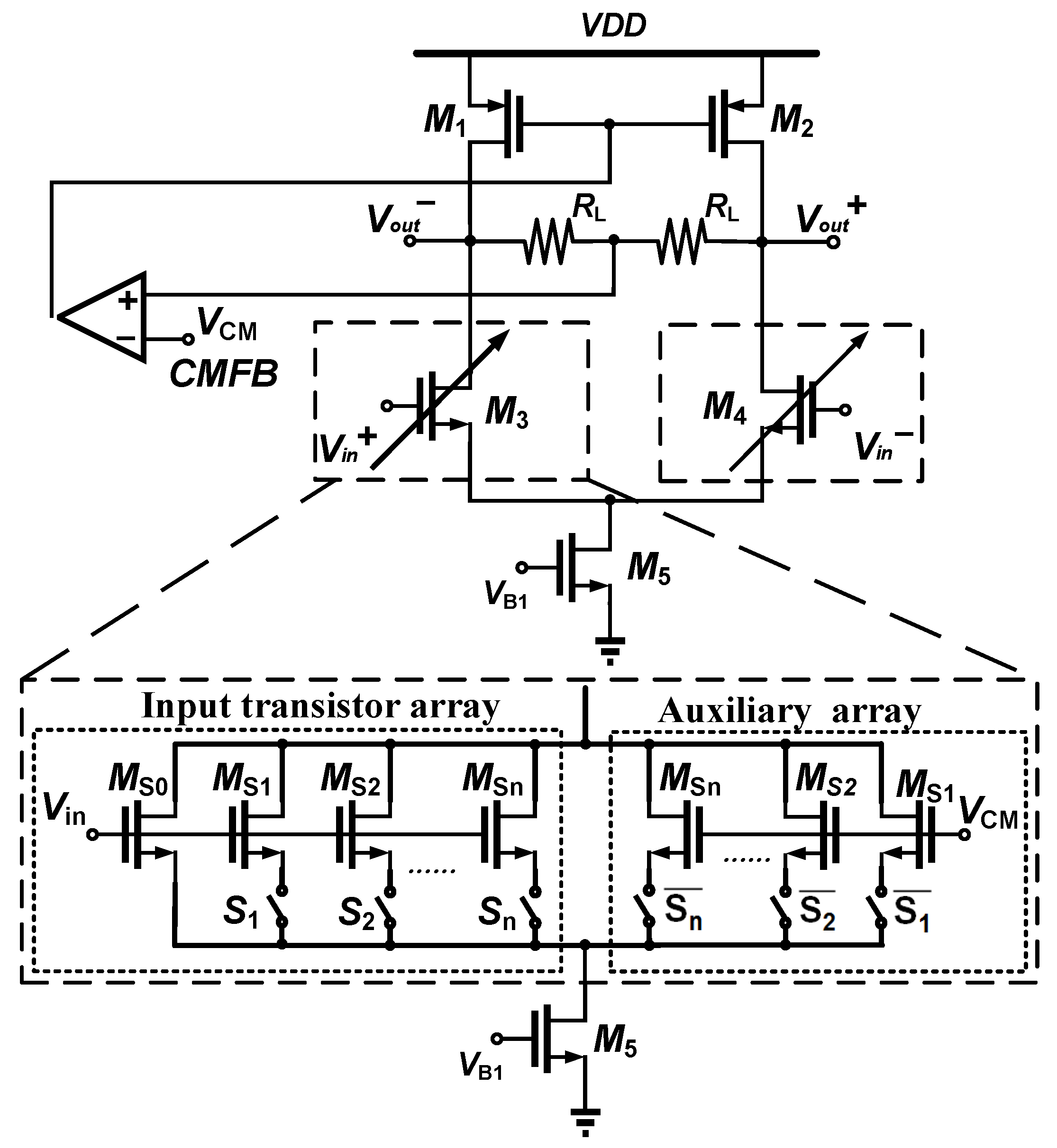
The rest gain cells (B-type gain cell) are common-source amplifiers using the constant current density function (
Figure 6) [
9]. Each B-type gain cell contains two transistor arrays (an input transistor array and an auxiliary array), connected in parallel, where each transistor in the arrays is connected with a switch in series. The switches controlled by the digital word
S1–Sn would be used to turn on or off the corresponding transistors M
S1–M
Sn in the input transistor array while the switches controlled by the digital word
would be used to turn on or off the corresponding transistors M
S1–M
Sn in the auxiliary array. In particular, the auxiliary array is applied with same input DC level (V
CM) and contains transistors identical to those in the input transistor array so that the output dc level can remain constant for each gain mode [
9].
If
KS0–
KSn represent the W/L ratios of the corresponding transistors M
S0–M
Sn, then the effective W/L ratio
Kn of the input transistor array can be expressed as:
The effective transconductance
gmn can be expressed as:
The gain equals the product of the effective transconductance
gmn and the load resistor
RL, and can be expressed as follows:
The voltage gain of each B-type gain cell can be varied from 0 to 7 dB in 1-dB steps. When all the gain cells are connected in cascade (as shown in
Figure 4), the gain range of 20 dB can be provided. During the simulation, the PGA delivers the voltage gain of 3.92 dB and −16.1 dB for the 5-bit binary programming word of 10,100 and 00,000, respectively.
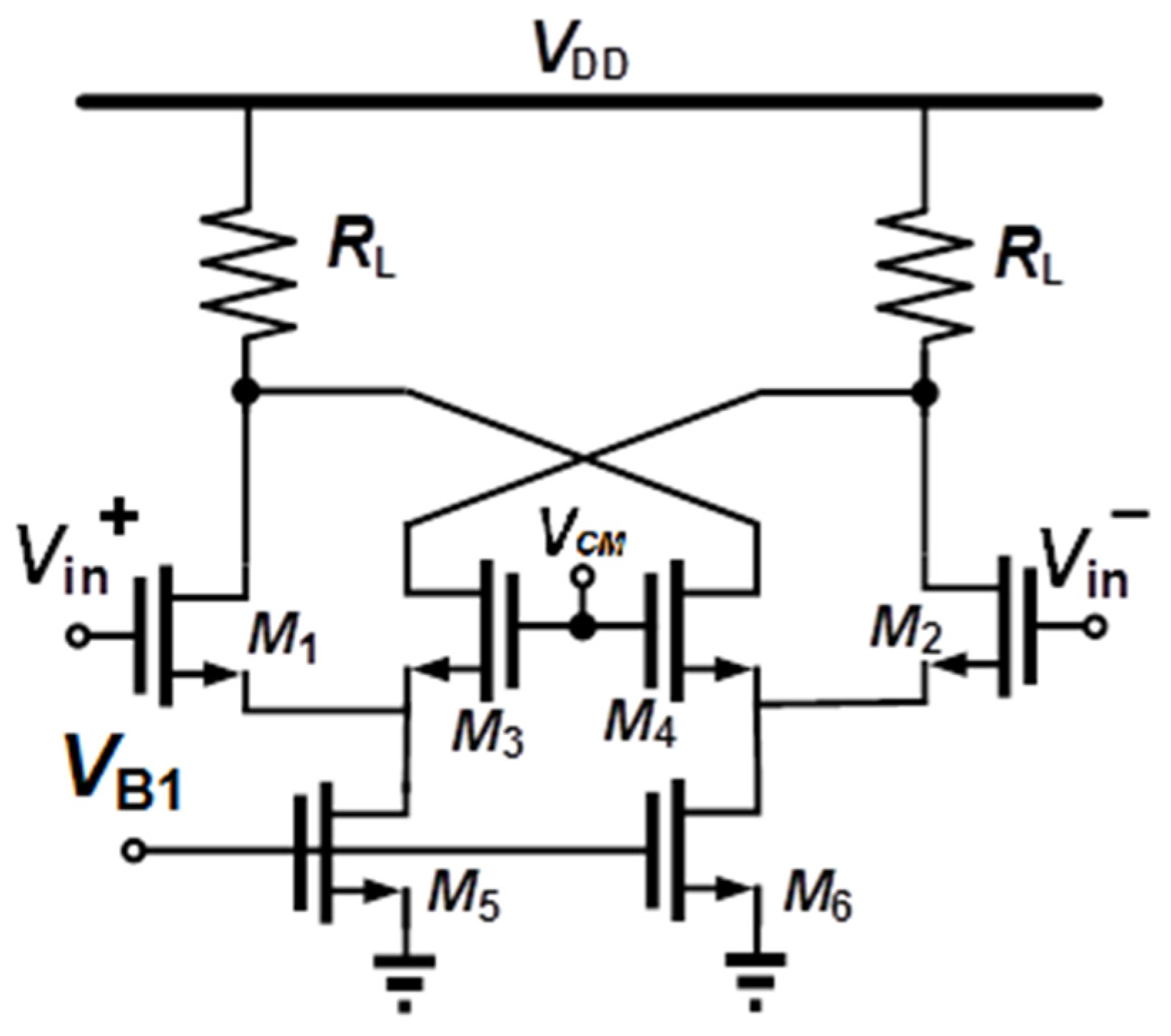
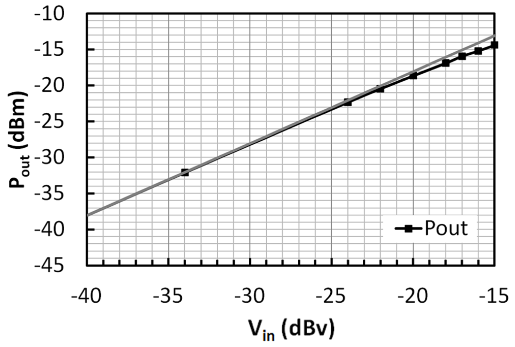
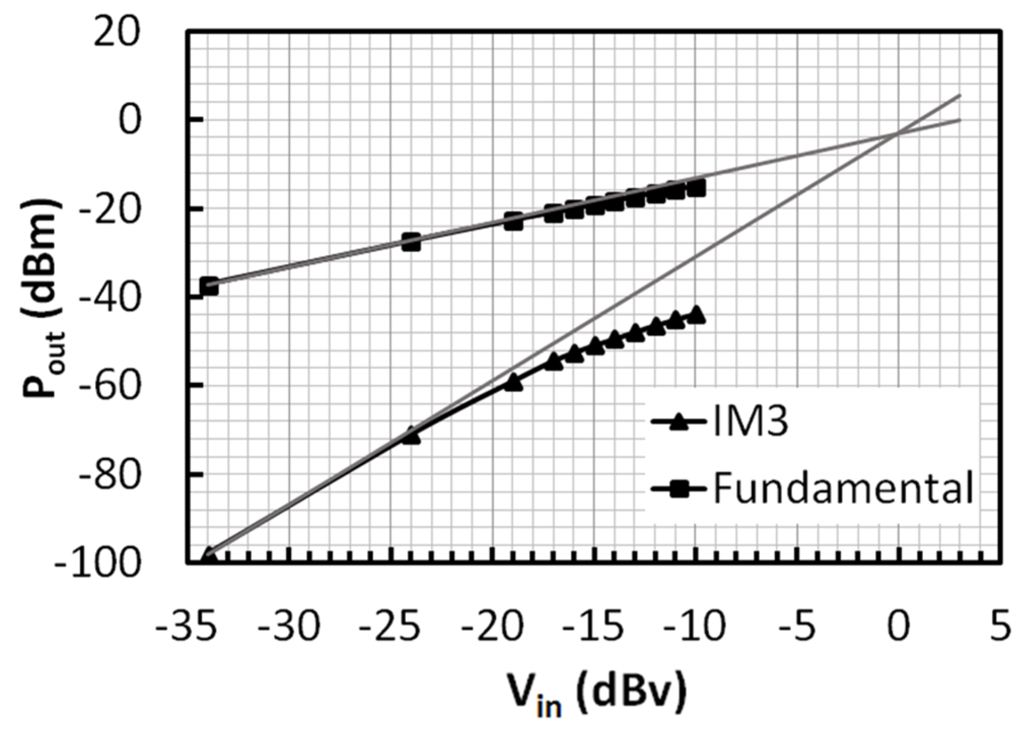
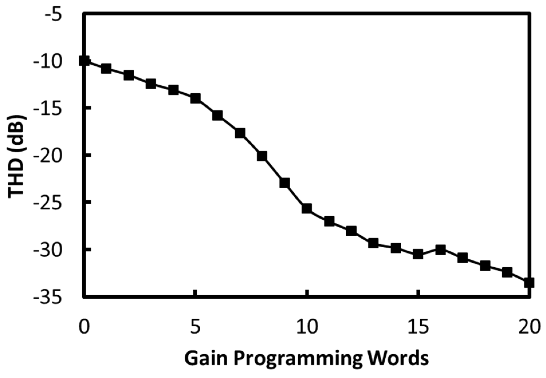
A buffer (
Figure 7) is used to drive the 50-Ω load of the network analyzer during the measurement. Moreover, it can also maintain the required bandwidth and linearity by minimizing the loading effect of the up-conversion mixer in the future. Based on the f
T-doubler architecture, the buffer delivers a high output current to extend the unit-gain frequency. During the simulation, the loading effect is considered by connecting an up-conversion mixer to the output of the buffer. According to the simulation, the buffer achieves the total harmonic distortion (THD) of −47 dB for the input level of 200 mV
pp and the 3-dB bandwidth of 1.7 GHz.
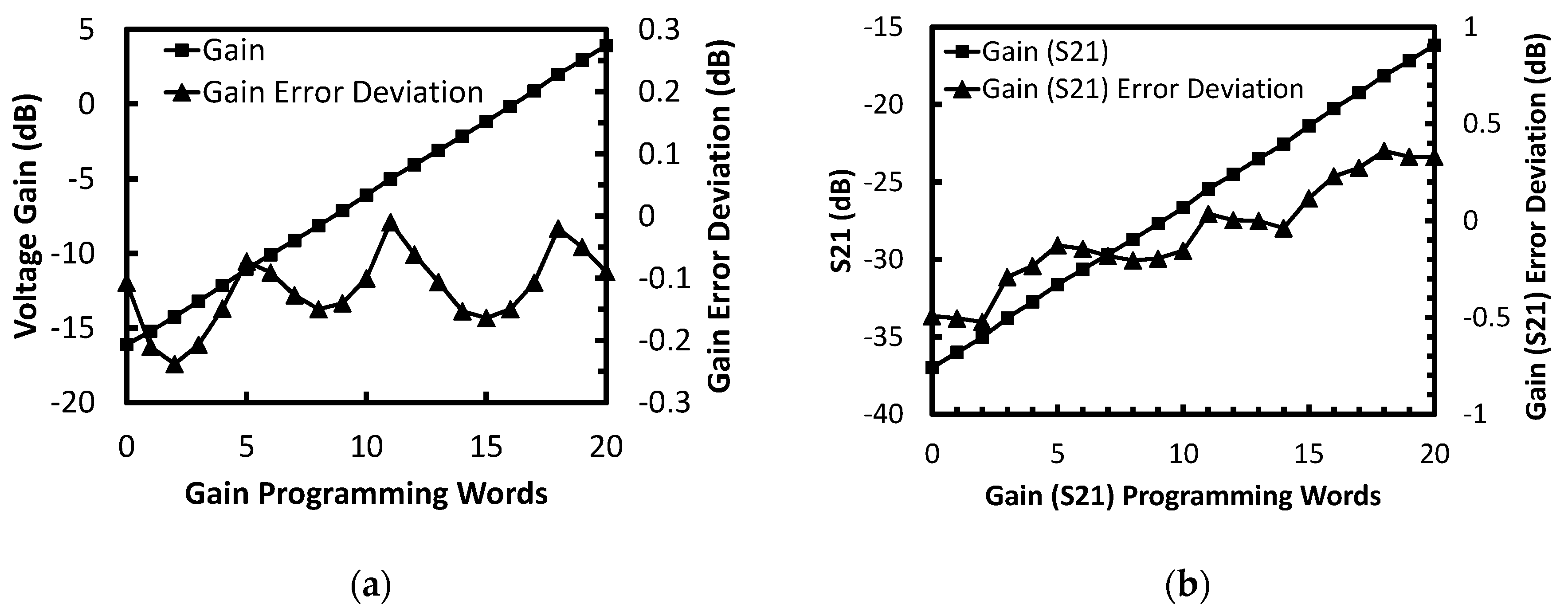
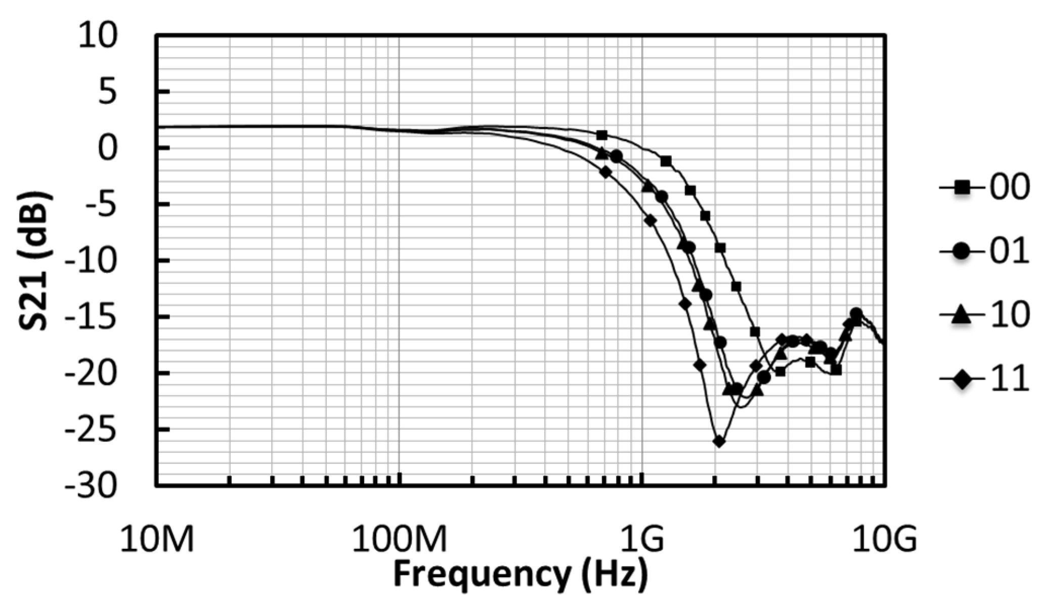
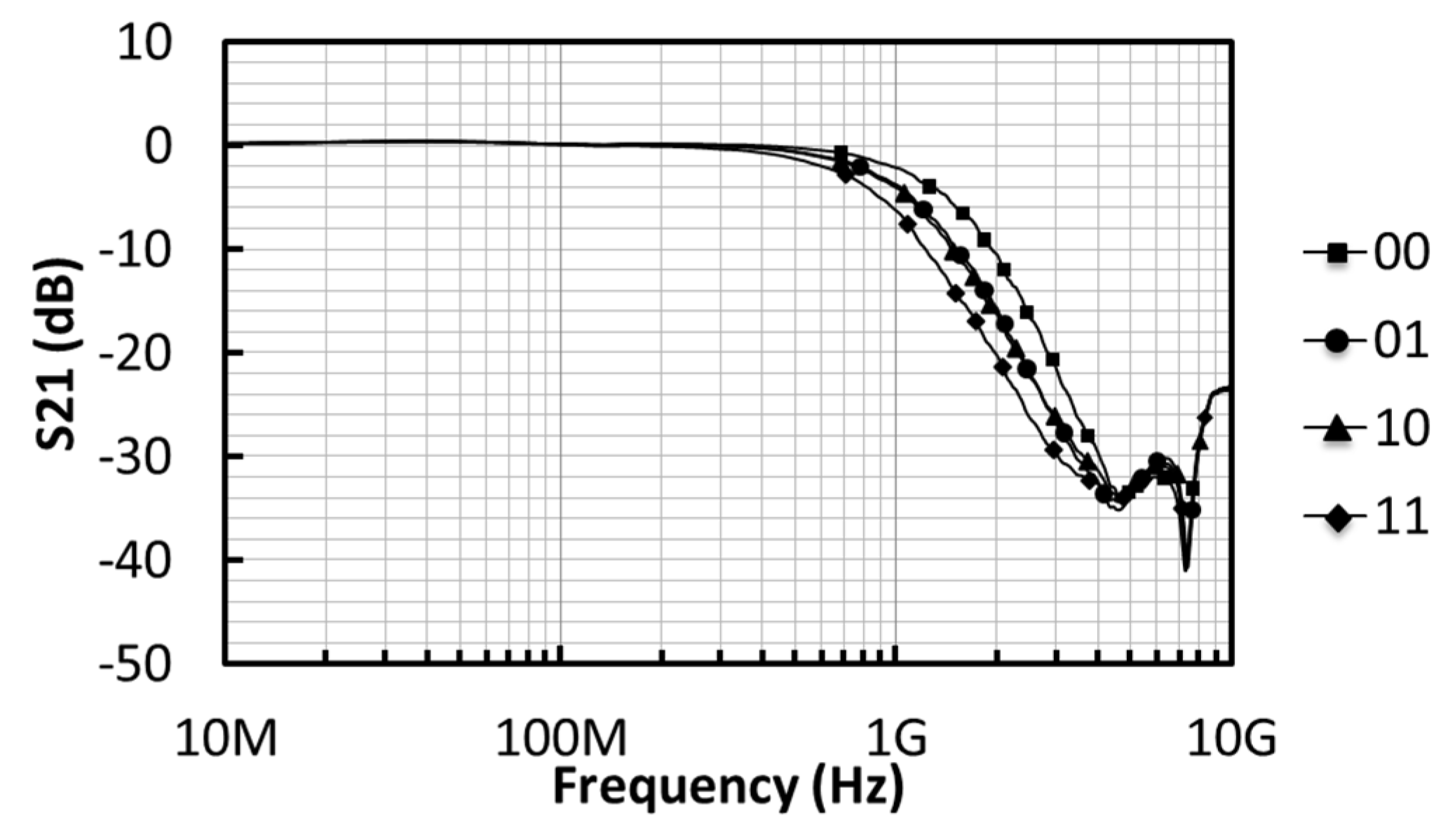
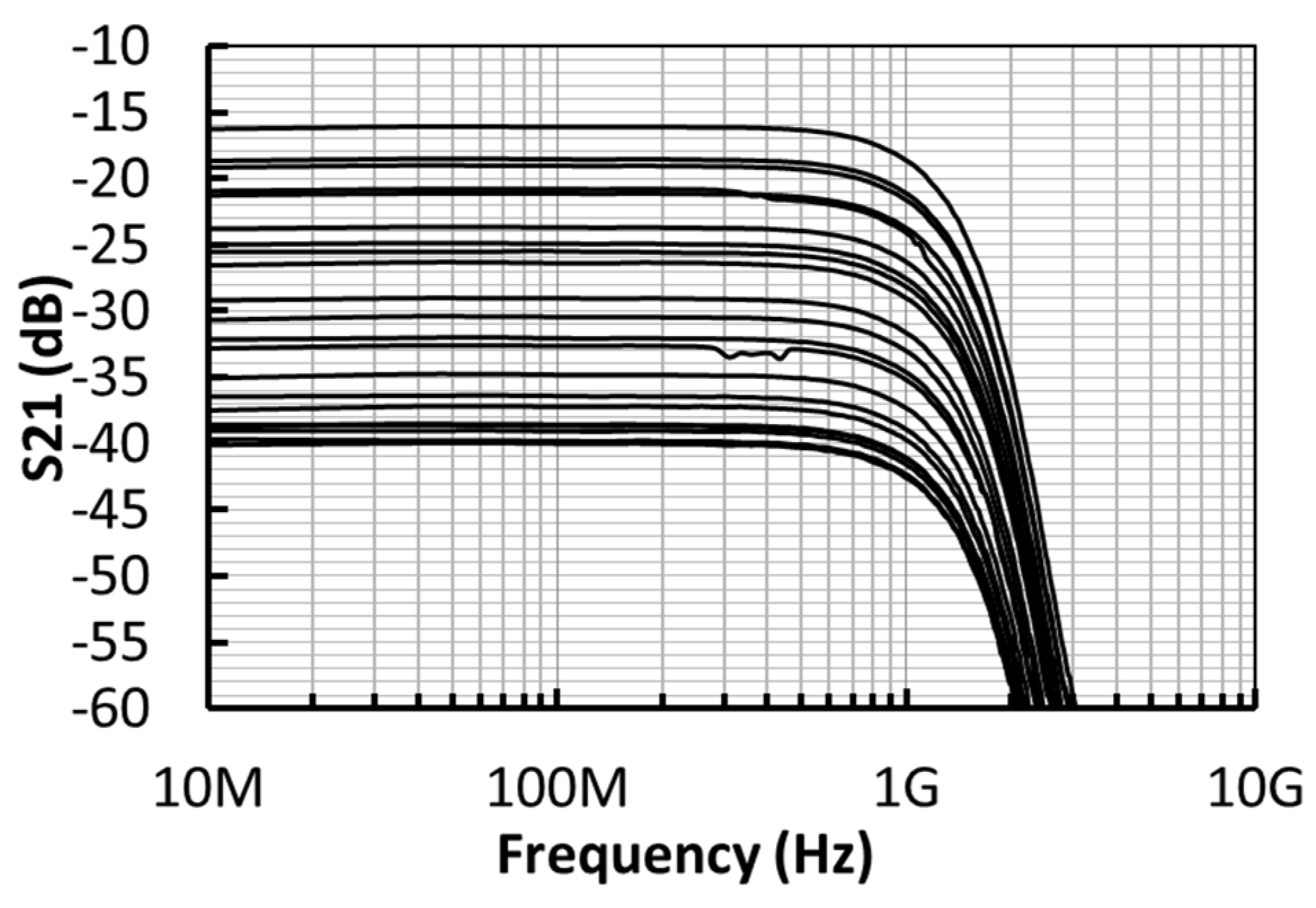
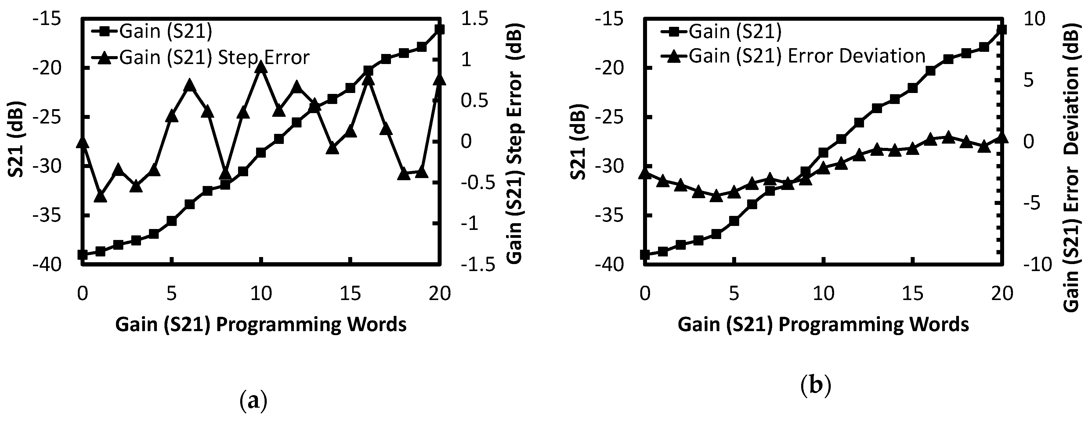
The frequency response of the PGA is observed in different gain modes during the simulation. The PGA exhibits the 3-dB bandwidth above 1.2 GHz in all the gain modes. The power gain S
21 is more available for the measurement with frequency range up to 1–2 GHz, while the voltage gain is specified as the requirement for analog baseband circuits, so the simulation is performed to observe both the voltage gain and power gain S
21. The simulation results of the voltage gain and gain error deviation in all the gain modes are shown in
Figure 8a. The gain step error is within ± 0.11 dB and the maximum gain error deviation is less than 0.23 dB. The simulation results of the S
21 and gain error deviations in all the gain modes are shown in
Figure 8b. The gain step error is within ± 0.23 dB and the maximum gain error deviation is less than 0.52 dB. According to the simulation results, the circuit delivers the voltage gain of 3.92 dB in the highest gain mode and the corresponding S
21 is −16.17 dB. In the lowest gain mode, the circuit delivers the voltage gain of −16.1 dB and the corresponding S
21 is −36.99 dB.
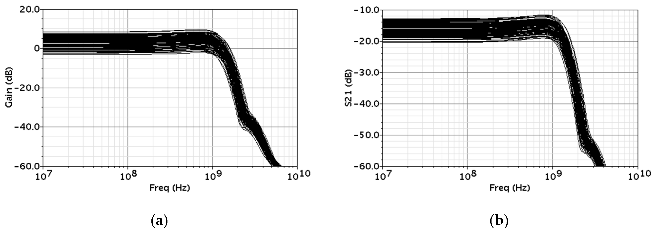
The Monte Carlo simulation results of the 5G transmitter (TX) analog baseband are shown in
Figure 9. Both the process variation and device mismatch are considered in the Monte Carlo simulation. The number of runs is set to 100 for the Monte Carlo simulation. The simulation results of the AC response in the highest gain mode are shown in
Figure 9a, where the gain variation is from −3.05 dB to 8.46 dB, and the corner frequency variation is from 1.12 MHz to 1.42 MHz. The simulation results of the S
21 in the highest gain mode are shown in
Figure 9b, where the gain variation is from −20.5 dB to −12.81 dB, and the corner frequency variation is from 1.211 MHz to 1.447 MHz.


