Article

A Complementary Recycling Operational Transconductance Amplifier with Data-Driven Enhancement of Transconductance †

Department of Precision Instruments, Tsinghua University, Beijing 100084, China
*
Authors to whom correspondence should be addressed.
This paper is an extended version of our previous conference paper: Li, X.; Wei, Q.; Zhou, B.; Chen, Z.; Zhang, R. Data-driven complementary recycling folded cascode OTA. In Proceedings of the International Conference on Mechanical, Electric and Industrial Engineering (MEIE), Hangzhou, China, 26–28 May 2018.
Electronics 2019, 8(12), 1457; https://doi.org/10.3390/electronics8121457
Submission received: 23 October 2019 / Revised: 25 November 2019 / Accepted: 28 November 2019 / Published: 1 December 2019
(This article belongs to the Section Microelectronics)

Abstract

:
An improved operational transconductance amplifier (OTA) is presented in this work. The fully differential OTA adopts the current recycling technique and complementary NMOS and PMOS input branches to enhance the total transconductance. Moreover, in order to achieve higher current efficiency, a data-driven biasing circuit was developed to dynamically adjust the power consumption of the amplifier. Two comparators were added to detect the voltage difference at the input nodes, and when the differential input is large enough to activate either comparator, extra biasing current is activated and poured into the amplifier to enhance its slew rate and gain-bandwidth product (GBW). The threshold voltage of the complementary recycling folded cascode (CRFC)-based comparator is configured to suppress overshoot. Complementary common-mode feedback (CMFB) topology with local CMFB structure is built to acquire high common-mode gain. The OTA was fabricated in SMIC 0.18- μ m CMOS technology. The experimental result based on a capacitive feedback loop shows that the data-driven operation improves the average slew rate of the amplifier from 10.2 V/ μ s to 55.5 V/ μ s while the power only increases by 150%. The OTA has good potential to satisfy the fast settling demands for capacitive sensing circuits.

1. Introduction

Operational transconductance amplifiers (OTAs) are widely used in capacitive sensor interface and switched capacitor circuits [1,2,3,4,5]. Enhancement of gain-bandwidth product (GBW), slew rate (SR) and current efficiency (CE) of OTA is required in application areas for large capacitive load, expeditious and accurate signal transition, and small power consumption. The folded cascode (FC) has been a fundamental amplifier structure to acquire high DC gain and relatively large signal swing [6,7], which is shown in Figure 1. However, it usually costs much biasing current since the cascode transistors are in separate current paths from the input transistors. Based on the current recycling technique by Assaad and Silva-Martinez [8,9], several approaches have been reported to enhance the transconductance and speed of OTA [10,11,12,13]. Although these techniques are beneficial for achieving higher and higher CE, the static biasing current remains a fixed power consumption contributor in a conventional class-A amplifiers. Considering the behaviour of a switched capacitor circuit for example, it generally consists of sampling stage and holding stage when triggered by a clock edge. To guarantee fast settling in sampling stage, the amplifier requires much biasing current to achieve high SR [14], but in the holding stage, it becomes unnecessary to maintain high SR and power consumption.
In this article, we demonstrate a data-driven complementary recycling folded cascode (CRFC) OTA for applications such as sensing and driving interfaces. The CRFC amplifier topology was developed to augment the GBW and make more efficient use of the current than the conventional recycling folded cascode (RFC) amplifier. Moreover, we established a data-driven scheme with a comparator-controlled extra current source branch added to the biasing circuit of the OTA. The data-driven current branch is activated and the extra current is poured into the biasing circuit to enhance the SR and GBW of the OTA and improve its speed when the input differential signal exceeds the comparator’s threshold voltage.
The article is organised as follows. In Section 2, the conventional FC and RFC architectures are analysed. In Section 3 the structure of the proposed CRFC amplifier is then described, and to improve its dynamic current efficiency, the data-driven scheme is introduced. The OTA was fabricated in SMIC 0.18 μ m technology. The simulated and experimental results are discussed in Section 4. Section 5 provides the conclusions.

2. Folded Cascode OTA and Recycling Technique

The conventional folded cascode (FC) OTA is shown in Figure 1. Two identical transistors M P 1 and M P 2 form differential input pair, and the cascode transistors M N 3 and M N 4 are in seperate current paths, which are "folded" to the drain nodes of M N 1 and M N 2 . The total current consumption is 4 I b , and the equivalent transconductance of the amplifier is
G m , F C = g m P 1 .
Under large signal input assumption, the SR of the FC amplifier can be expressed as
S R F C = 2 I b C L .
The FC is regarded as one of the most significant amplifier architectures for its high gain and relatively large signal swing [15]. However, as the cascode transistors consume biasing current independently, they suffer the disadvantage of power inefficiency. To enhance the transconductance of the FC, Assaad and Silva-Martinez [8,9] introduced the recycling technique and realised the recycling folded cascode (RFC) amplifier shown in Figure 2. The input transistors are split in half, and the transistors M N 1 and M N 2 in Figure 1 are modified to current mirrors which have a ratio of 3:1. The total current of the RFC is 4 I b , equal to the FC. The small signal currents are amplified by the current mirrors to get enhanced transconductance, which can be derived as
G m , R F C = ( 1 + 3 ) g m P 1 a = 4 g m P 1 a ,
where 2 g m P 1 a = g m P 1 . And the SR of RFC is
S R R F C = 6 I b C L .
Compared with Equations (1) and (2), it can be seen that the RFC has an enhanced transconductance by a factor of 2 and a slewrate larger by a factor of 3 than the FC under equal biasing current conditions.

3. Proposed Data-Driven CRFC OTA

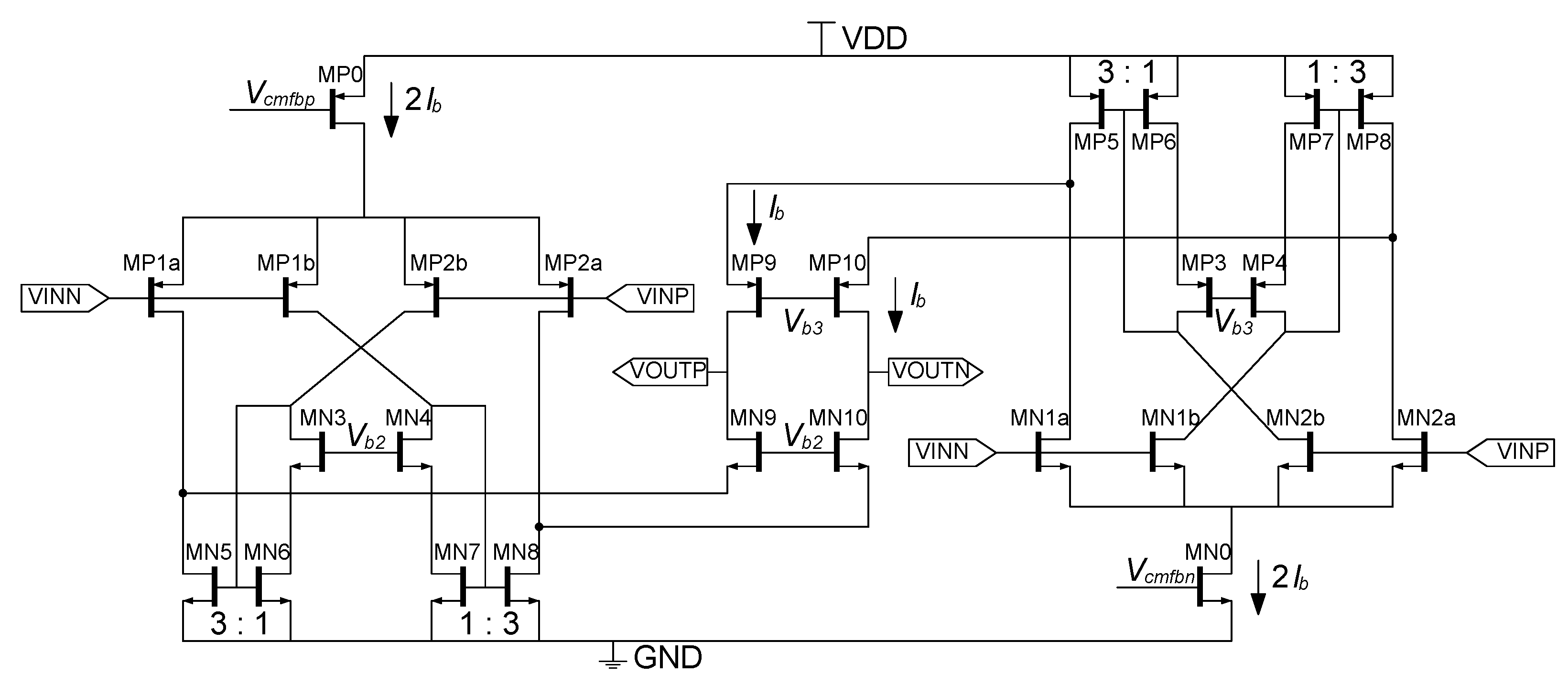
3.1. CRFC Amplifier Circuit

We introduced a CRFC [16] architecture as the main part of the amplifier, shown in Figure 3. This structure was developed from the idea of recycling current of a folded cascode [8,9]. As opposed to the PMOS-input-only RFC amplifier in Figure 2, an NMOS-input branch formed by transistors M N 1 a , M N 1 b , M N 2 a and M N 2 b is added parallel to the PMOS-input one. The cascode transistors of each branch ( M N 9 and M N 10 for the PMOS input, M P 9 and M P 10 for the NMOS input) share the same current path, and the total current flowing through the folded cascode transistors is 2 I b . The biasing current of either input drivers, i.e., the drain current of M P 0 or M N 0 , is also equal to 2 I b , so the total static current of the CRFC amplifier is 6 I b . The transconductance of the amplifier can be written as
G m , C R F C = 4 g m P 1 a + 4 g m N 1 a ,
and the slew rate of the full-differential output can also be derived as
S R C R F C = 12 I b C L .
Since for a transistor in strong inversion region, whether P-type or N-type, g m / I D is only relevant to V G S V T , we can reasonably assume the PMOS and NMOS input transistors have the equal transconductance. It can be found that the transconductance and the slew rate of the CRFC amplifier is twice that of the conventional RFC while the current consumption increases by a half. If we define two F o M s (figures of merit) to characterise the amplifiers’ performance as
F o M 1 = G B W × C L I ,
F o M 2 = S R × C L I ,
we can find F o M 1 , C R F C = 4 F o M 1 , R F C / 3 and F o M 2 , C R F C = 4 F o M 2 , R F C / 3 , which indicates the current efficiency of the CRFC is improved by a factor of 1/3 compared with the RFC, with the same capacitive load. The symmetry of the circuit with complementary input differential pairs also provides larger input swing.

3.2. Data-Driven Biasing Scheme

The biasing circuit with data-driven scheme for the CRFC amplifier [16] is shown in Figure 4. The current mirrors formed by transistors M 1 M 24 and the current source I 1 compose conventional biasing circuit. Under this biasing circumstance, the amplifier will operate at a fixed static current level. The transconductance and SR of the OTA are limited by Equations (5) and (6), which means that higher speed can only be achieved by increasing the aspect ratio of the transistors, and thus consuming more power. In order to explore a method to mitigate the conflict between performance and power dissipation, a data-driven control method is implemented to the biasing circuit.
A parallel current source I 2 with two NMOS switches M S 1 and M S 2 was added to the biasing circuit. The gate of each switch is connected to the output terminal of one comparator. The absolute difference of input signal of the OTA is also monitored by the comparators. If the differential input signal is large enough to drive either comparator to flip, for example, letting V I N P larger than V I N N , the output voltage of C O M P 1 will be pulled to V D D and switch M S 1 will be turned on. Then, current source I 2 will be activated in the biasing circuit and the total current of the amplifier is augmented, enhancing the transconductance and slew rate. When the input signal gets smaller than the comparators’ threshold, both comparators are pulled down to zero voltage and shut off the switches. Only current source I 1 provides biasing, and the amplifier consumes relatively little power. However, stability and accuracy of the circuit are retained due to better phase margin at this static state. We take the switched capacitor circuit as an application example. At the sampling stage, the data-driven option is activated and the transition speed be improved, while at holding stage, the amplifier works at low-power state preserving high DC gain and accuracy. Through the dynamic biasing accommodation method, a higher average current efficiency will be achieved. The data-driven biased amplifier was inspired by a common digital circuit [17]. The voltage difference between two differential input nodes is sampled to generate one-bit signal to control the analogue biasing condition. Still, it should be underlined that the proposed amplifier has two different biasing current levels. When designing the transistors’ parameters, the operating points of static mode and data-driven mode should be considered simultaneously to retain good performance at both working states.
Figure 5 shows the comparator circuit used in the data-driven part. Latch-based structure is widely used in data converters [18]. However, extremely high comparator gain is not preferred in this design, since a very small input signal will trigger the data-driven operation, leading to large power consumption and signal distortion. The comparator based on the CRFC technique was chosen, modifying the full-differential topology to single-end output. The threshold of comparator should also be carefully designed to select an optimised shifting point between small-current and large-current states. We configured the threshold several millivolts over zero to reduce overshoot when switching from data-driven mode to static mode. We reduced the aspect ratio of transistor M C 0 to pull up the drain voltage of M C 18 and M C 20 with zero differential input signal. When V C N V C P > V t h r e s , the drain voltage of M C 18 comes below the turning point of the inverter, causing the comparator output V C O U T set to 1. Through this configuration, the operating window of the data-driven scheme can be controlled to satisfy specific requirements.

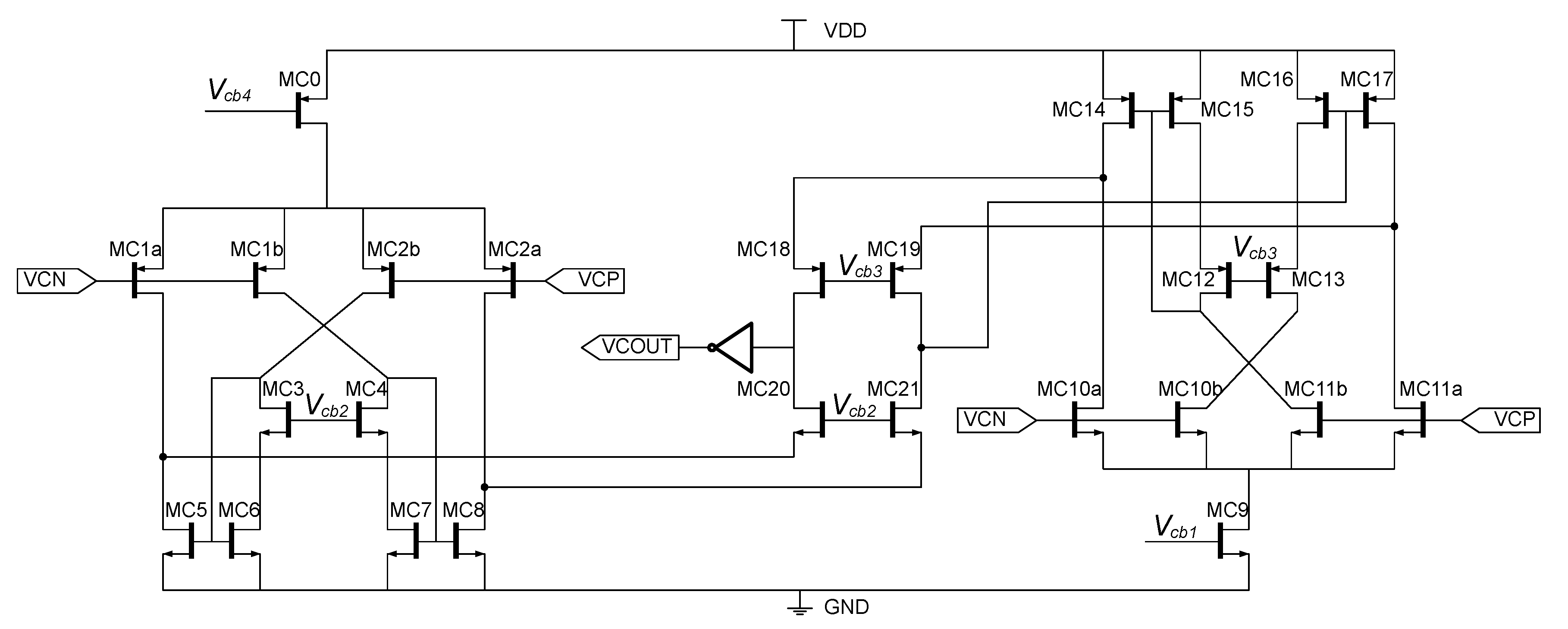
3.3. Common-Mode Feedback (CMFB) Realisation

The full-differential OTA requires a common-mode feedback circuit (CMFB) to settle the common-mode voltage of both output points. In order to avoid signal glitch and aliasing, we established a continuous-time CMFB architecture based on the idea in [19] for the CRFC amplifier, which is shown in Figure 6: a complementary CMFB circuit which has two separate branches to provide biasing for both NMOS and PMOS current sources in the CRFC amplifier (see Figure 3). Each branch in the proposed CMFB circuit applies a local CMFB structure which consists of two MOS transistors and two matched resistors in series, which, taking the V c m f b p -output branch as an example, enlarges the transconductance by a factor of g m P 0 R , where g m P 0 is the transconductance of M P 0 in the CRFC amplifier’s main circuit. By using this CMFB module, a larger GBW can be achieved and the dynamic performance is improved.

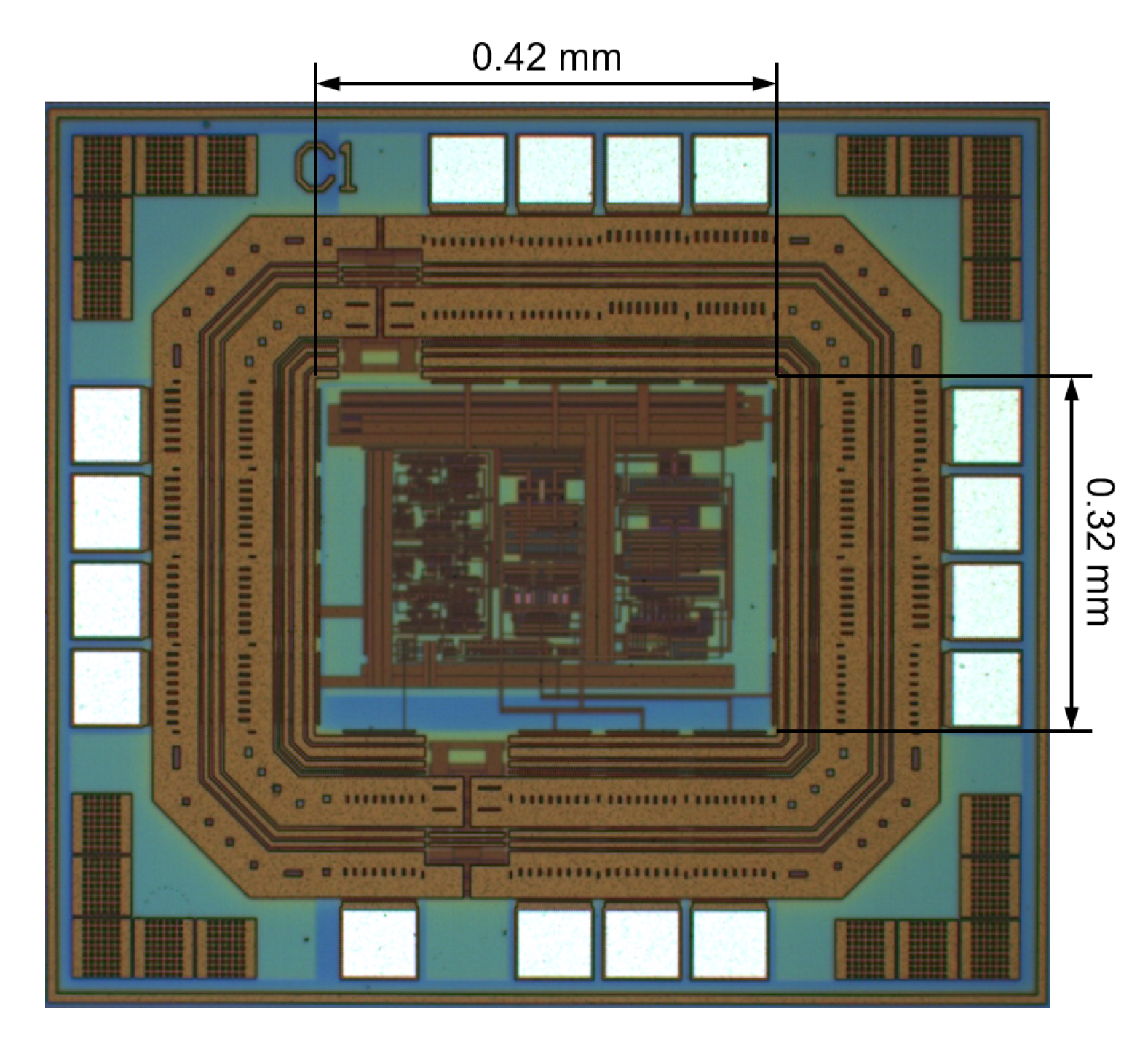
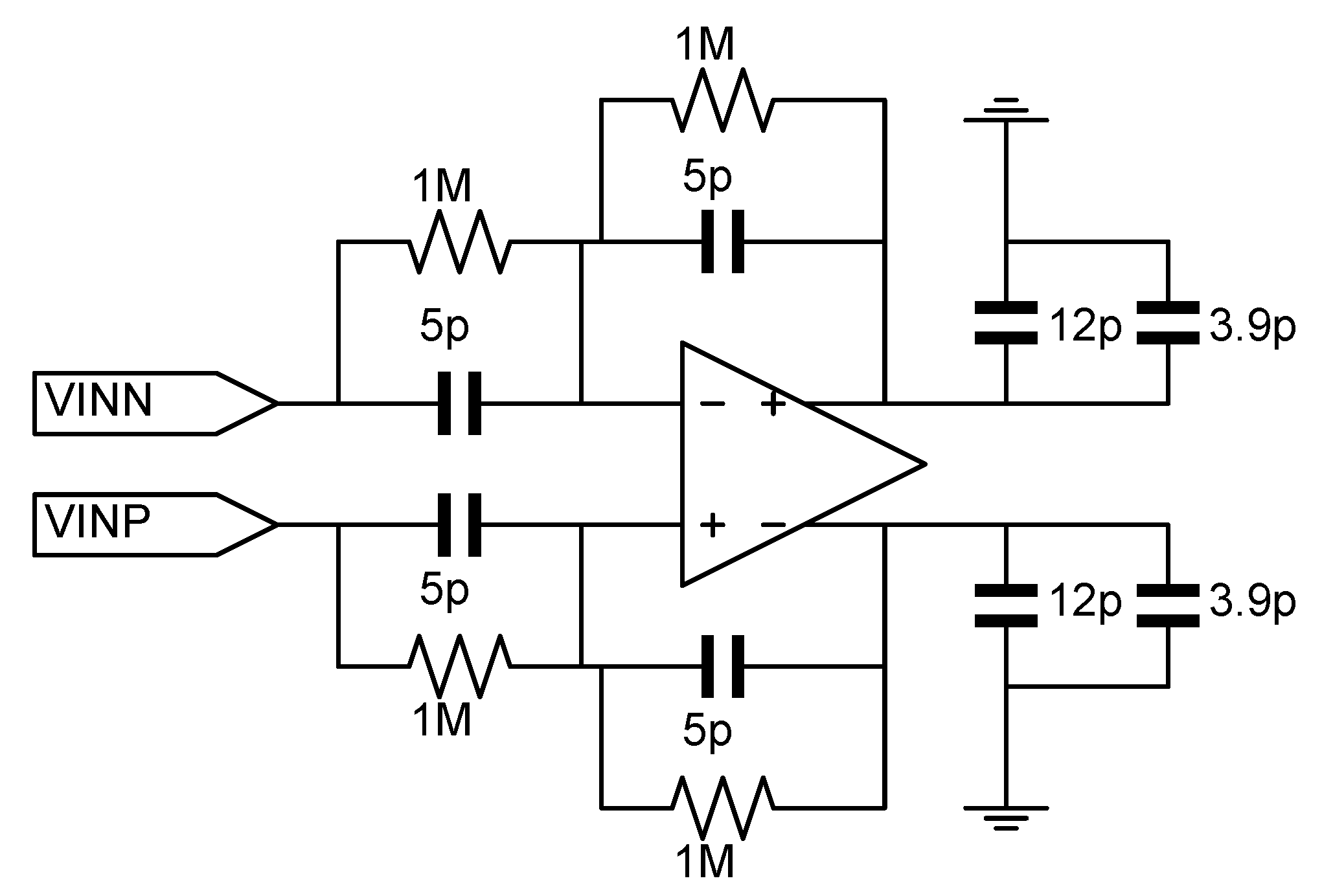
4. Simulation and Experimental Results

The amplifier was designed and fabricated in an SMIC 0.18- μ m mixed-signal CMOS process, and the chip’s micro-photograph is shown in Figure 7. The core part of the amplifier occupied 0.42 × 0.32 mm 2 . The DC supply voltage for the circuit was 5 V. Selection logic was added to choose whether the data-driven function turns on.
First, open loop AC response of the designed OTA at static mode and data-driven mode was simulated respectively, shown in Figure 8. At static mode, when the amplifier works at low current standard, the DC gain is 61.0 dB and the GBW is 17.5 MHz with a phase margin of 58.5 . In data-driven mode, the DC gain slightly decreases to 59.2 dB, but the GBW increases to 49.2 MHz with a phase margin of 57.0 . This can be explained by the theoretical model of a single transistor, for which, as current increases, transconductance gets higher while small-signal resistance gets smaller, leading to the degradation of DC gain.
A unity gain capacitive feedback circuit was set up as a test bench for characterising the amplifier’s performance, as Figure 9 shows. The input and feedback capacitors were 5 pF, and there was 12 pF of capacitive load at each output terminal. Besides, Tektronix MDO3034 oscilloscope was used to detect the output signal, with 3.9 pF of the probe. The overall load was 18.4 pF approximately. A pair of differential square signals with a peak-to-peak voltage of 1 V and frequency of 800 kHz was applied to the input terminals, and transient waveform of the differential output was sampled by the oscilloscope, as Figure 10 shows. For the CRFC amplifier biased in static mode, the rising times were 403 and 379 ns with a total average current of 530 μ A, and the average calculated SR was 10.2 V/ μ s. Meanwhile, for the circuit with the data-driven scheme activated, decreased rising times of 79 and 65 ns were recorded and the average SR was 55.5 V/ μ s with an average current consumption of 1320 μ A. Note that the measured current included the main amplifier circuit, biasing current mirrors, common-mode feedback circuit and comparators (only in data-driven mode). It was found that in this test, the data-driven operational cost was about 150% extra current. The increased part of power dissipation came from the voltage-controlled current source and the comparators. However, an enhancement about 440% in speed was achieved, indicating that adopting the data-driven scheme improved the total current efficiency, even counting the added current consumption.
The results of the proposed amplifier are summarised in Table 1 (compared with previous reported OTAs). Assaad et al. first reported the recycling current technology [8,9], based on which Yan et al. [10], Akbari [11] and Zhao et al. [13] did significant works to improve the performance of single-stage OTAs. Designed for applications such as capacitive sensor interfaces, DC supply voltage of 5 V was selected to guarantee driving capability and preserve accuracy [20]. Since the transistors operating at this supply level were relatively slower than low-voltage counterparts in general, the amplifier presented in this work had smaller F o M s. However, previous simulation results using low voltage transistors [16] indicated the architecture proposed could achieve very high F o M s. The comparison of the proposed amplifier between static mode and data-driven mode should be emphasised more; it indicated that the idea of dynamically adjusting the biasing current introduced in this work improved the current efficiency over conventional class-A amplifiers significantly, making a novel attempt at digital control in the field of OTAs. It should also be noted that the efficiency improvement was achieved at the cost of more area occupation, mainly taken by the comparators. And to avoid performance degradation when switching between static mode and data-driven mode, the transistors in the main amplifier circuit should be more carefully designed, which increases design difficulties.

5. Conclusions

In this paper, an improved operational transconductance amplifier with a data-driven transconductance enhancement method was presented. The complementary recycling architecture was adopted to achieve a better transconductance and power efficiency. The data-driven method adopted the digital control idea to accommodate the biasing current of amplifier dynamically, and to achieve both augmented slew rate and speed significantly when the amplifier deals with large input. Experimental results confirmed the performance improvement through the data-driven operation. It was an attempt to combine digital thought with a basic analogue circuit block, opening a path to acquiring high performance and low power usage simultaneously. This kind of amplifier has great potential for applications such as capacitive sensing and switched capacitor circuits.

Author Contributions

Conceptualisation, Q.W., B.Z., and R.Z.; methodology, Q.W., B.Z. and R.Z.; validation, X.L., B.H. and C.J.; formal analysis, X.L., B.H. and C.J.; investigation, X.L., B.H. and C.J.; resources, Q.W., B.Z. and R.Z.; data curation, X.L.; writing—original draft preparation, X.L., B.H., C.J., Q.W., B.Z. and R.Z.; writing—review and editing, X.L., B.H., C.J., Q.W., B.Z. and R.Z.; visualisation, X.L. and B.H.; supervision, Q.W., B.Z. and R.Z.; project administration, Q.W. and B.Z.; funding acquisition, Q.W., B.Z. and R.Z.

Funding

This research was funded by the National Natural Science Foundation of China (grant number 41871245) and the National High Technology Research and Development Program of China (“863” program, grant number 2013AA014103).

Acknowledgments

The authors would like to acknowledge support from Beijing Innovation Centre for Future Chips, Tsinghua University.

Conflicts of Interest

The authors declare no conflict of interest.

References

  1. Singh, T.; Saether, T.; Ytterdal, T. Current-Mode Capacitive Sensor Interface Circuit With Single-Ended to Differential Output Capability. IEEE Trans. Instrum. Meas. 2009, 58, 3914–3920. [Google Scholar] [CrossRef]
  2. Naderi, M.H.; Prakash, S.; Silva-Martinez, J. Operational Transconductance Amplifier With Class-B Slew-Rate Boosting for Fast High-Performance Switched-Capacitor Circuits. IEEE Trans. Circuits Syst. I Regul. Pap. 2018, 65, 3769–3779. [Google Scholar] [CrossRef]
  3. Sun, J.; Rahkonen, T. Speed-Up Technique by Pre-Charging Load Capacitor in a SC Residue Circuit. IEEE Trans. Circuits Syst. II Express Briefs 2019, 66, 522–526. [Google Scholar] [CrossRef]
  4. Petkov, V.P.; Boser, B.E. A fourth-order ΣΔ interface for micromachined inertial sensors. IEEE J. Solid State Circuits 2005, 40, 1602–1609. [Google Scholar] [CrossRef]
  5. Mojarad, M.; Kamarei, M. Low-voltage high-gain large-capacitive-load amplifiers in 90-nm CMOS technology. AEU Int. J. Electron. Commun. 2015, 69, 666–672. [Google Scholar] [CrossRef]
  6. Lee, J.; Song, S.; Roh, J. A 103 dB DR Fourth-Order Delta-Sigma Modulator for Sensor Applications. Electronics 2019, 8, 1093. [Google Scholar] [CrossRef]
  7. Bano, S.; Narejo, G.B.; Ali Shah, S.M.U. Power Efficient Fully Differential Bulk Driven OTA for Portable Biomedical Application. Electronics 2018, 7, 41. [Google Scholar] [CrossRef]
  8. Assaad, R.; Silva-Martinez, J. Enhancing general performance of folded cascode amplifier by recycling current. Electron. Lett. 2007, 43, 1243. [Google Scholar] [CrossRef]
  9. Assaad, R.S.; Silva-Martinez, J. The Recycling Folded Cascode: A General Enhancement of the Folded Cascode Amplifier. IEEE J. Solid State Circuits 2009, 44, 2535–2542. [Google Scholar] [CrossRef]
  10. Yan, Z.; Mak, P.I.; Martins, R.P. Double recycling technique for folded-cascode OTA. Analog Integr. Circuits Signal Process. 2012, 71, 137–141. [Google Scholar] [CrossRef]
  11. Akbari, M. Single-stage fully recycling folded cascode OTA for switched-capacitor circuits. Electron. Lett. 2015, 51, 977–979. [Google Scholar] [CrossRef]
  12. Aghaee, T.; Biabanifard, S.; Golmakani, A. Gain boosting of recycling folded cascode OTA using positive feedback and introducing new input path. Analog Integr. Circuits Signal Process. 2017, 90, 237–246. [Google Scholar] [CrossRef]
  13. Zhao, X.; Zhang, Q.; Wang, Y.; Deng, M. Transconductance and slew rate improvement technique for current recycling folded cascode amplifier. AEU Int. J. Electron. Commun. 2016, 70, 326–330. [Google Scholar] [CrossRef]
  14. Yin, S.; Sun, Y.; Li, X. Digital 1 V 82 μW Pseudo-Two-Stage Class-AB OTA. Tsinghua Sci. Technol. 2009, 14, 601–605. [Google Scholar] [CrossRef]
  15. Sansen, W.M.C. Analog Design Essentials; Springer: Berlin/Heidelberg, Germany, 2006. [Google Scholar]
  16. Li, X.; Wei, Q.; Zhou, B.; Chen, Z.; Zhang, R. Data-driven complementary recycling folded cascode OTA. In Proceedings of the International Conference on Mechanical, Electric and Industrial Engineering, Hangzhou, China, 26–28 May 2018. [Google Scholar]
  17. Crovetti, P.S. A Digital-Based Analog Differential Circuit. IEEE Trans. Circuits Syst. I Regul. Pap. 2013, 60, 3107–3116. [Google Scholar] [CrossRef]
  18. Shen, J.; Shikata, A.; Fernando, L.D.; Guthrie, N.; Chen, B.; Maddox, M.; Mascarenhas, N.; Kapusta, R.; Coln, M.C.W. A 16-bit 16-MS/s SAR ADC With On-Chip Calibration in 55-nm CMOS. IEEE J. Solid State Circuits 2018, 53, 1149–1160. [Google Scholar] [CrossRef]
  19. Lopez-Martin, A.; Garde, M.; Ramirez-Angulo, J. Class AB differential difference amplifier for enhanced common-mode feedback. Electron. Lett. 2017, 53, 454–456. [Google Scholar] [CrossRef]
  20. Hou, B.; Li, C.; Gao, Z.; Wei, Q.; Zhou, B.; Zhang, R. Design, Optimization, and Compensation of a High-Precision Single-Excitation Absolute Capacitance Angular Encoder up to ±4. IEEE Trans. Ind. Electron. 2019, 66, 8161–8171. [Google Scholar] [CrossRef]
Figure 1. Conventional folded cascode operational transconductance amplifiers (OTA).
Electronics 08 01457 g001
Figure 2. The recycling folded cascode (RFC) OTA.
Electronics 08 01457 g002
Figure 3. The complementary recycling folded cascode (CRFC) OTA [16].
Electronics 08 01457 g003
Figure 4. Biasing circuit with the data-driven scheme [16].
Electronics 08 01457 g004
Figure 5. Comparator circuit based on CRFC structure.
Electronics 08 01457 g005
Figure 6. Complementary common-mode feedback circuit (CMFB) circuit.
Electronics 08 01457 g006
Figure 7. The chip’s micro-photograph, showing the core part and surrounding I/O pads.
Electronics 08 01457 g007
Figure 8. AC response of proposed amplifier in static and data-driven modes.
Electronics 08 01457 g008
Figure 9. Test bench setup for characterising the amplifier’s performance.
Electronics 08 01457 g009
Figure 10. Transient response waveforms of the proposed OTA. (a) The CRFC amplifier in static mode with an average slew rate (SR) of 10.2 V/ μ s; and (b) the data-driven scheme enabled amplifier with an average SR of 55.5 V/ μ s.
Electronics 08 01457 g010
Table 1. Performance comparison.
Parameter[9][10][11][13]This Work
StaticData-Driven
DC supply (V)1.811.2155
Current ( μ A)400800483405301320
Capacitive load (pF)5.61053018.418.4
GBW (MHz)70.4203.265010.217.583
Phase margin ( )79.866.25080.458.566.2
DC gain (dB)59.754.559.180.370.261.0
Average SR (V/ μ s)48.191.6115.21.7810.255.5
FoM 1 (MHz·pF/mA)985.6254062797650607.51157
FoM 2 ((V/ μ s)pF/mA)673.4114511931335354.1773.6

