Article

A 2.6 GS/s 8-Bit Time-Interleaved SAR ADC in 55 nm CMOS Technology

1
Institute of Microelectronics of the Chinese Academy of Sciences, Beijing 100029, China
2
School of Microelectronics, University of Chinese Academy of Sciences, Beijing 100049, China
*
Author to whom correspondence should be addressed.
Electronics 2019, 8(3), 305; https://doi.org/10.3390/electronics8030305
Submission received: 9 February 2019 / Revised: 2 March 2019 / Accepted: 6 March 2019 / Published: 8 March 2019
(This article belongs to the Special Issue Signal Processing and Analysis of Electrical Circuit)

Abstract

:
This paper presents an eight-channel time-interleaved (TI) 2.6 GS/s 8-bit successive approximation register (SAR) analog-to-digital converter (ADC) prototype in a 55-nm complementary metal-oxide-semiconductor (CMOS) process. The channel-selection-embedded bootstrap switch is adopted to perform sampling times synchronization using the full-speed master clock to suppress the time skew between channels. Based on the segmented pre-quantization and bypass switching scheme, double alternate comparators clocked asynchronously with background offset calibration are utilized in sub-channel SAR ADC to achieve high speed and low power. Measurement results show that the signal-to-noise-and-distortion ratio (SNDR) of the ADC is above 38.2 dB up to 500 MHz input frequency and above 31.8 dB across the entire first Nyquist zone. The differential non-linearity (DNL) and integral non-linearity (INL) are +0.93/−0.85 LSB and +0.71/−0.91 LSB, respectively. The ADC consumes 60 mW from a 1.2 V supply, occupies an area of 400 μm × 550 μm, and exhibits a figure-of-merit (FoM) of 348 fJ/conversion-step.

1. Introduction

High-speed analog-to-digital converters (ADCs) with a moderate resolution of 6–8 bits while maintaining excellent power efficiency for longer battery life are highly demanded for applications such as 802.11 ad (WiGig) radio architectures and the next-generation mobile communication system (5G) [1]. Compared with flash and pipeline ADC, successive approximation register (SAR) ADC has superior energy efficiency and is more suitable for the aggressive downscaling of technology because of its primarily digital nature [2,3,4]. In order to overcome the speed limitation of a single ADC, time-interleaved (TI) architecture running multiple parallel ADCs is an attractive approach. In general, TI SAR ADC is the most feasible solution to realize both over GHz operation and medium resolution around 8-bit [5]. However, the inter-channel non-ideal factors like offset, gain mismatch, and time skew, will deteriorate the overall performance [6], and can be compensated for by either circuit improvement in the analog domain or special digital calibration. As digital calibration is often complex, it is preferred to minimize these mismatches using on-chip design optimization to relax calibration requirements, especially when the number of interleaved channels is not large.
This paper demonstrates a 2.6 GS/s 8-bit SAR ADC prototype with an eight-channel direct sampling TI architecture. In the sampling front-end, in order to suppress the time skew error among different channels, the channel-selection-embedded bootstrap switch is used as the sampling switch to ensure the uniformity of sampling times by the master clock. In the sub-channel SAR ADC design, segmented pre-quantization and a bypass switching scheme is employed to avoid unnecessary large capacitors switching, reducing power consumption and non-linearity. Double comparators clocked asynchronously in alternate mode are used to improve the conversion rate, with the background offset calibration function integrated on-chip. This ADC exhibits lower calibration complexity and achieves an acceptable efficiency in terms of area and power consumption.

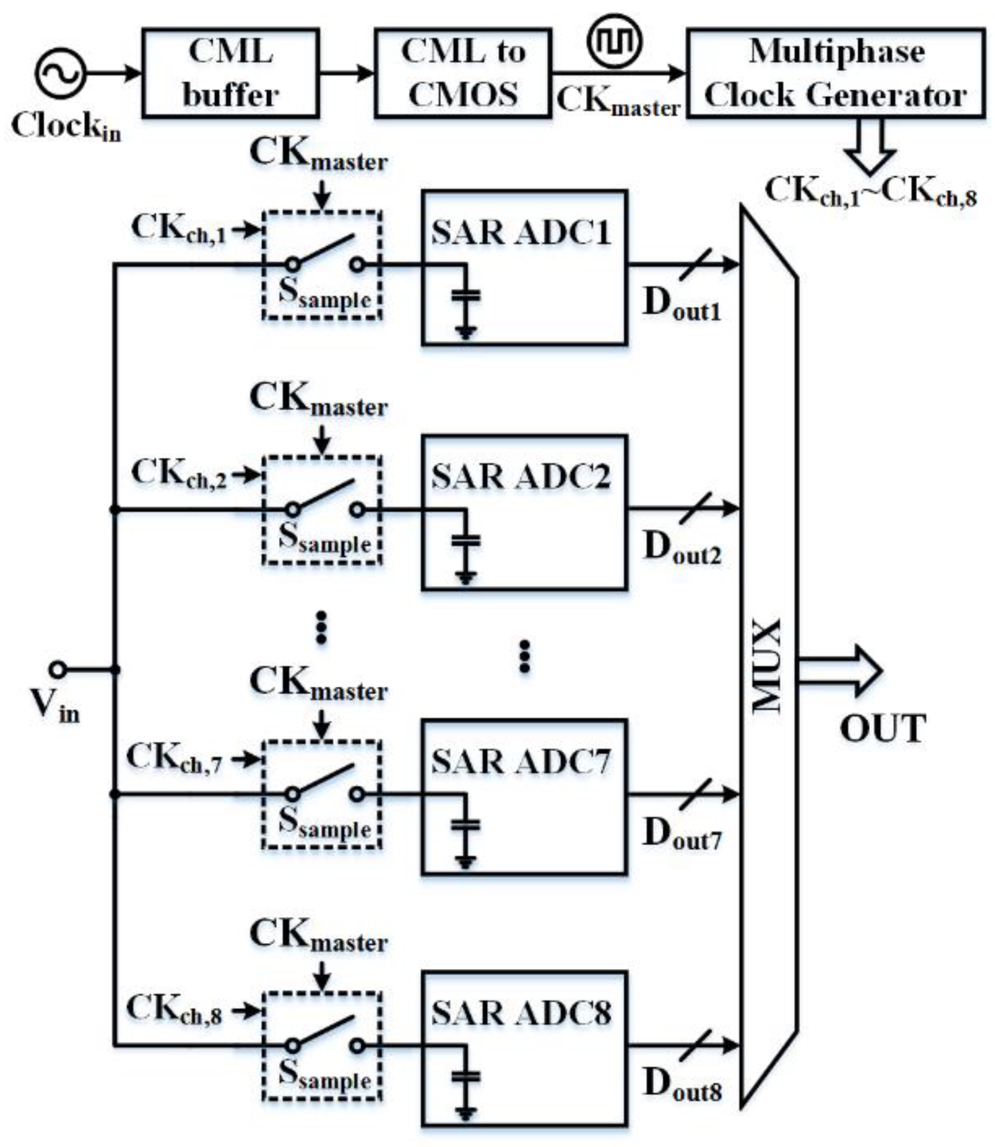
2. Proposed TI SAR ADC Architecture

TI structures can generally be categorized as hierarchical sampling and direct sampling. In a hierarchical sampling structure, there are at least two sampling switches in series in each sub-channel. In contrast, a direct sampling architecture, wherein all parallel channels have individual sample/hold circuits, provides the shortest signal transmission path from the input to the sampling capacitors, and is very efficient for a small number of parallel channels (usually ≤8) [7].
In this design, a direct sampling architecture is adopted to implement the 2.6 GS/s 8-bit TI ADC prototype, which mainly consists of multi-phase clock generator (MPCG), sampling switch, eight-channel 325 MS/s 8-bit SAR ADC, and multiplexer (MUX), as depicted in Figure 1.
The current-mode logic (CML) sinusoidal input clock signal is buffered and then transformed to complementary metal-oxide-semiconductor (CMOS) level full-speed master clock CKmaster. The multi-phase clock pulse signals CKch,1CKch,8 are generated from CKmaster using the cascaded D flip-flop (DFF) chain [8,9,10] and combinational logic circuits using synchronous frequency division, as shown in Figure 2a.
The DFF is constructed using two latches [11], as shown in Figure 2b. The internal signals q1, q2, q3 and q4 with a duty cycle of 50% are the divide-by-eight clocks of CKmaster such that a clock pulse signal CKdiv8 with a duty cycle of 12.5% is obtained through AND logic operation. Since the initial state of the shift registers is uncertain, the feedback logic is added to activate self-starting such that the MPCG can automatically return from the non-ideal state to normal. The shift operation of CKdiv8 is executed to get CKch,1CKch,8, which have definite phase sequence relationships and the delay between each other is one period of CKmaster, as shown in Figure 2c. The non-overlapping sampling phases guarantee that only one sampling switch is turned on, thus reducing the channel load at the input. CKch,1CKch,8 are not only used as the control signals for the sampling switches, but also initiate the conversion process of each channel.
As the input signal is sampled onto the capacitors array of respective sub-ADC sequentially for quantization, the sampling instants are controlled uniformly using CKmaster to mitigate the time skew between channels. Finally, the multi-path digital outputs from the sub-ADCs array are aggregated into a one-way data stream using MUX.

3. Circuit Implementation Details

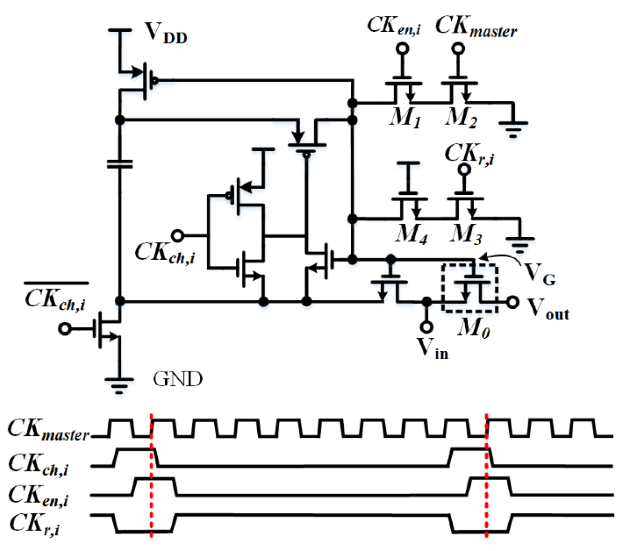
3.1. Channel-Selection-Embedded Bootstrap Switch

Time skew refers to the mismatch in the sampling instants among TI channels, which originated from the non-uniform sampling clock edges [12]. Some timing-skew, calibration-free techniques have been proposed to suppress the time skew by circuit design and layout [13,14,15]. We attempted to realize similar skew tolerance via circuit improvement in the analog domain for design simplicity rather than digital calibration with complex algorithms that will consume extra hardware and power. The channel-selection-embedded bootstrap switch [16] is utilized in the sampling front-end, so that the sampling instants of each channel are aligned to the master clock CKmaster, while the corresponding TI clock signals CKch,i (i = 1–8) are used to perform the channel selection, as described in Figure 3.
When CKch,i becomes high, the switching transistor M0 is turned on, and the channel begins to track the input signal. CKen,i is a delayed version of CKch,i, used to prepare for sampling synchronization. When CKen,i is high, once the rising edge of CKmaster comes, M1 and M2 are both turned on, and the gate voltage VG of M0 is released from Vin + VDD to the ground level, thus the sampling instants are determined by the rising edge of CKmaster. Then, the channel finishes the sampling process and enters the holding phase. As CKen,i goes low, the gate of M0 is in floating state and vulnerable to the interference of other signals. M3 from CKr,i provides a discharging path, and the VG is fixed to the ground level, therefore avoiding the floating node at the holding phase. The inter-channel sampling synchronization that is determined uniformly by CKmaster ensures the consistency of the sampling instants, and it is beneficial to suppress the time skew among channels.

3.2. Sub-ADC Design

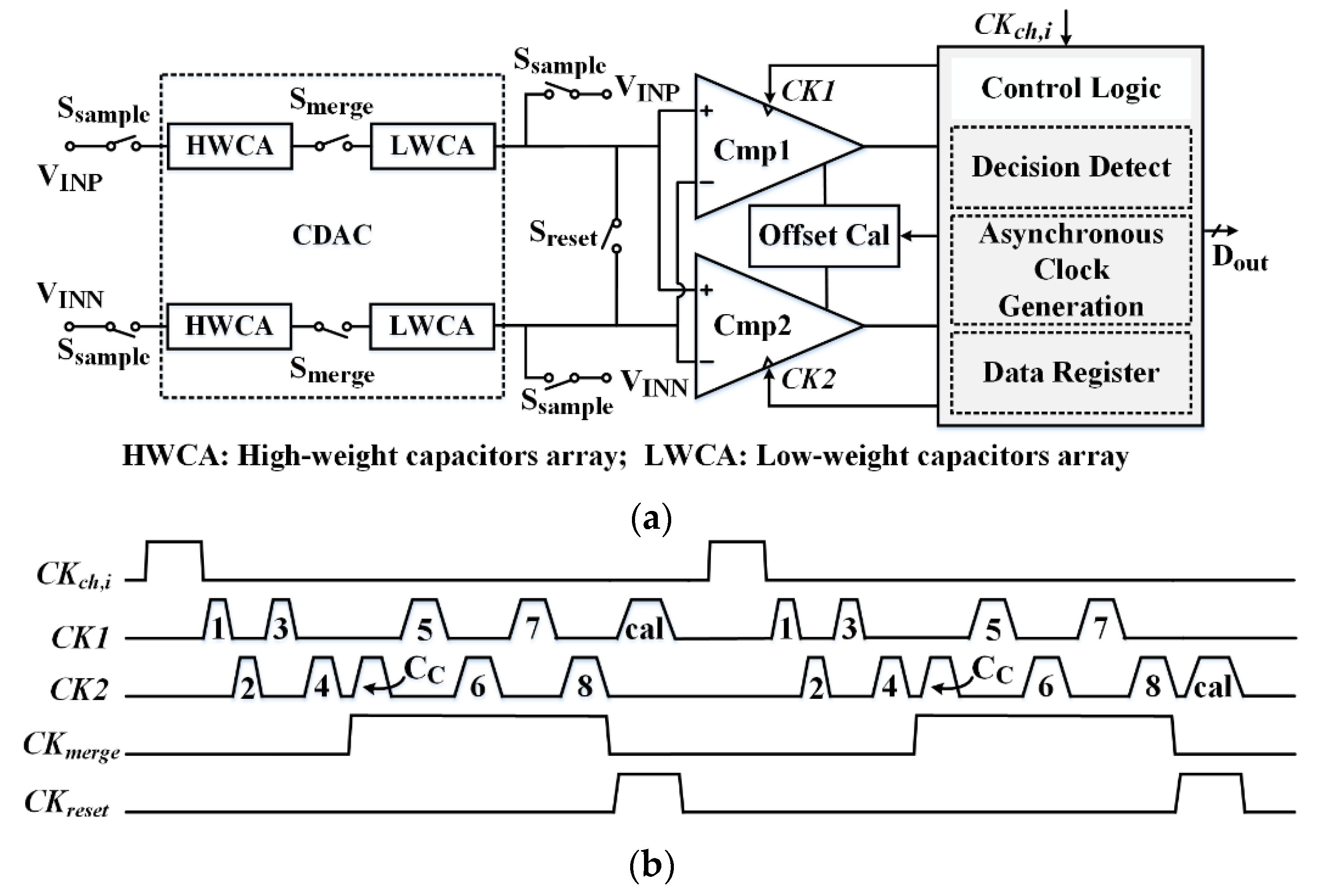
3.2.1. Asynchronous Timing of Alternate Comparators

The sub-ADC is implemented with 325 MS/s 8-bit SAR ADC [17], including fundamental building blocks, such as capacitive digital-to-analog converter (CDAC), comparators and control logic, as illustrated in Figure 4a.
If only one comparator is used in the SAR ADC, the comparator needs to be fully reset to avoid the residual effect from the previous conversion process, so the overall conversion speed is slowed down. Double dynamic comparators with cross-coupled latches are used [18], and the preamplifier has been designed for moderate gain to reduce its offset, and more importantly, to limit the kick-back noise from the latch [19]. The two comparators are clocked asynchronously in alternate operation, as shown in Figure 4b. Under the control of CK1 and CK2, when one comparator is in a comparison state, another comparator is reset, reducing the impact of reset time on the critical path, and thus improving the conversion speed [20]. Once the preceding comparison is over, a successful decision is detected as the trigger signal for the following comparison process. This asynchronous conversion process repeats like dominoes until all bits are resolved [21].
The pulse labeled “CC” corresponds to the operation for the compensation capacitor in the CDAC. At the end of the conversion, the inputs of the comparators are shorted together using CKreset for calibration purposes. With the pulse labeled “cal” the background offset calibration based on the charge pump principle in the analog domain for each comparator is carried out once every two cycles.

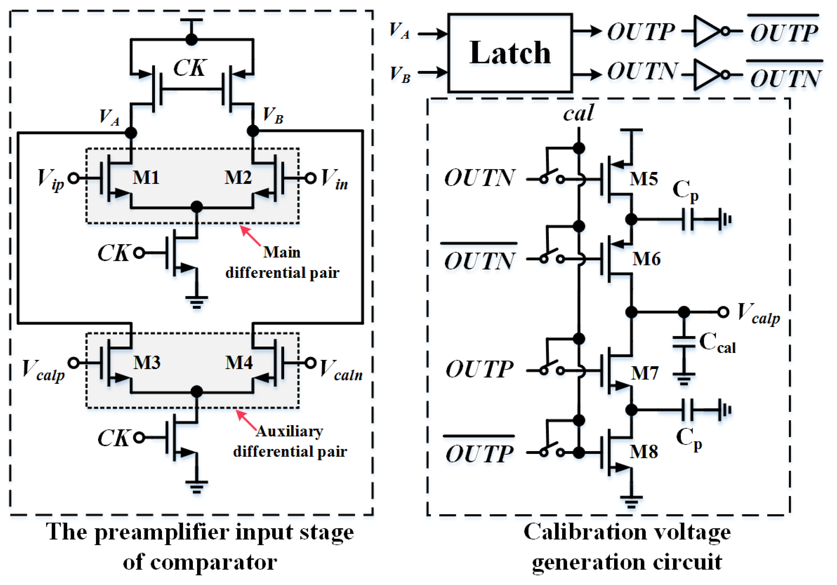
3.2.2. The Background Offset Calibration of Comparator

The diagram of comparator’s background offset calibration is shown in Figure 5. An auxiliary differential pair is introduced to calibrate the offset voltage of the comparator. Only the generation circuit of Vcalp is presented. Another calibration voltage Vcaln can be generated in two ways, one is set to a constant voltage using a resistive voltage divider [20], and the other is similar to the generation of Vcalp, except that the corresponding control voltage is different. In this design, the latter method is adopted. Vcalp and Vcaln change in opposite directions and jointly cancel the impact of the offset.
During the offset calibration phase of the comparator, the input signals Vip and Vin of the main differential pair are shorted together. In the case of no offset, Vip = Vin, then the output voltage of the preamplifier stage is equal, that is, VA = VB. Finally, the output signal of the comparator OUTP = OUTN = 0, and the corresponding complementary output signal O U T P ¯ = O U T N ¯ = 1 . At this time, M5 and M8 are on, the upper capacitor Cp is charged to the power supply, and the lower Cp is discharged to the ground level. Both M6 and M7 are off, and the calibration voltage Vcalp remains unchanged. There is no calibration effect yet.
If the offset exists, OUTP or OUTN will change. Usually, the output changes caused by offset can be equivalent to the input changes. Taking an offset output case as an example, if OUTP = 0 and OUTN = 1, this offset effect is the same as the situation when Vip < Vin. Note that VA > VB now. In the calibration voltage generation circuit, M6 is turned on, the voltage on Cp charges Ccal, and Vcalp is pumped up. Then Vcalp is fed back to the preamplifier input stage such that VA decreases to approximate VB. After a number of calibration cycles, once the decreasing VA is equal to VB, OUTP = OUTN, thereby realizing offset calibration. The calibration step size or accuracy is related to the capacitance values of Cp and Ccal. The parasitic capacitor can be used as Cp, which is usually small. The larger the calibration capacitor Ccal, the higher the calibration accuracy and the better the calibration effect. However, a large Ccal will affect the calibration settling time, and a trade-off between calibration accuracy and settling time is required to determine the value of Ccal.

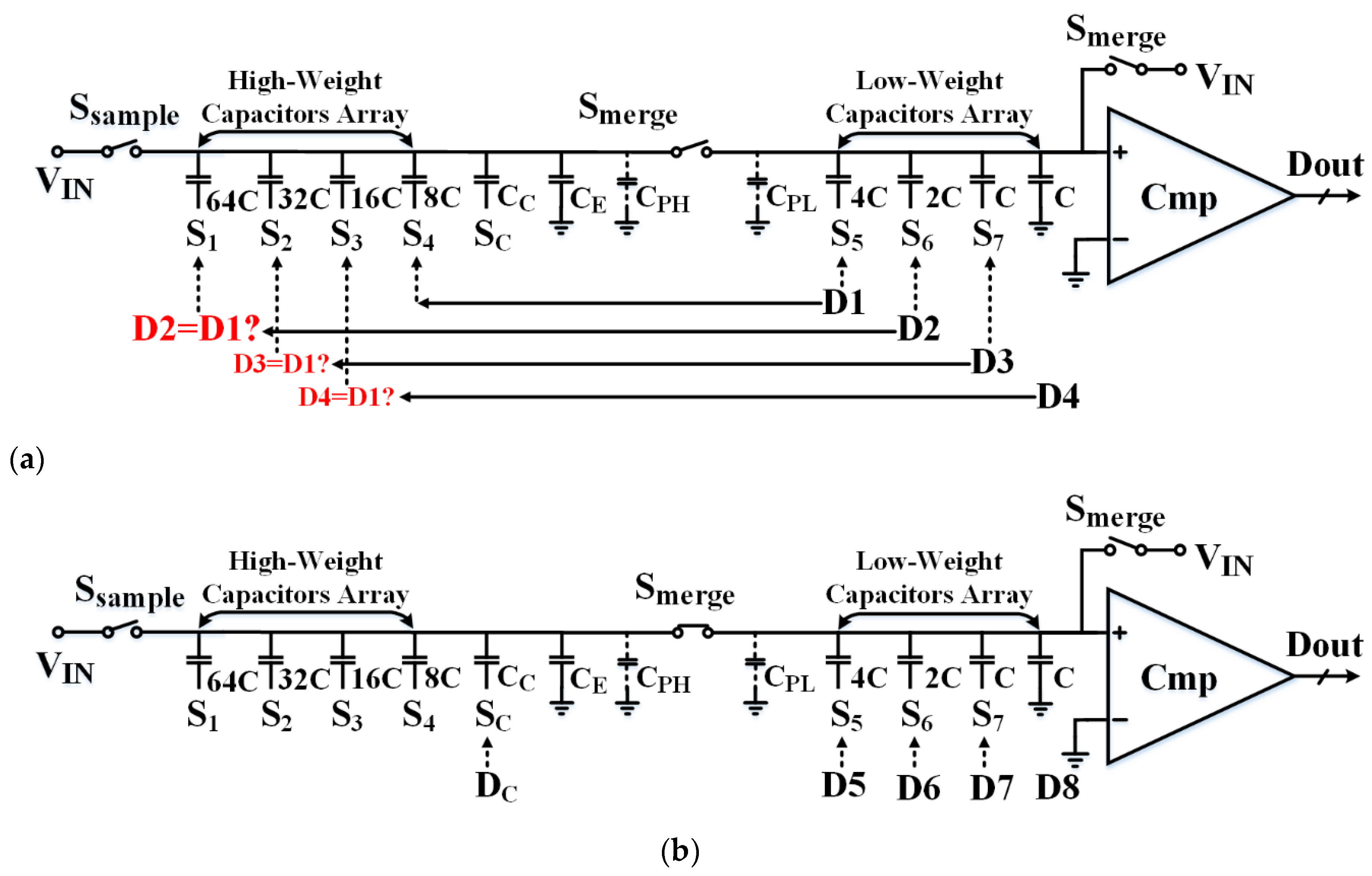
3.2.3. Segmented Pre-Quantization and Bypass Switching Scheme
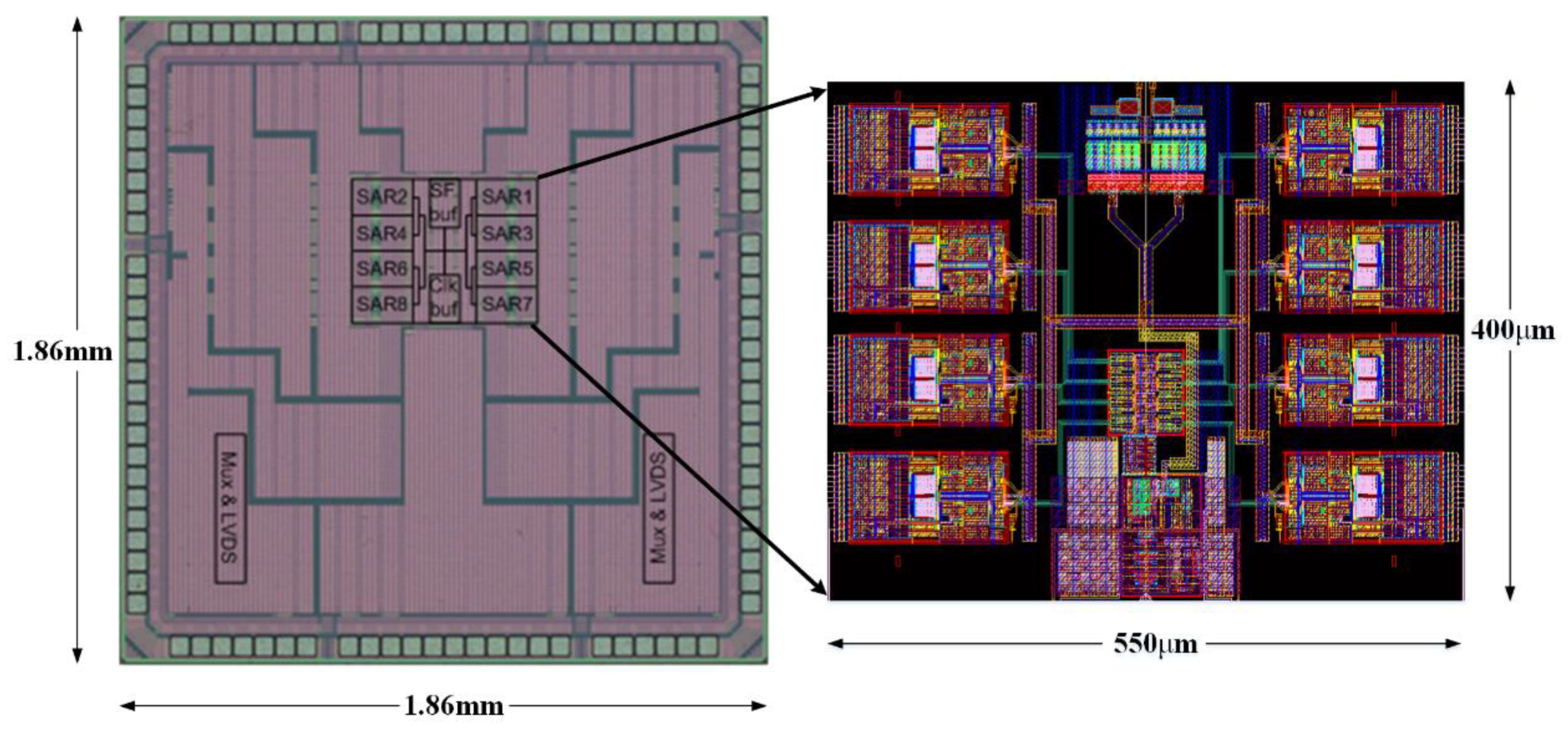
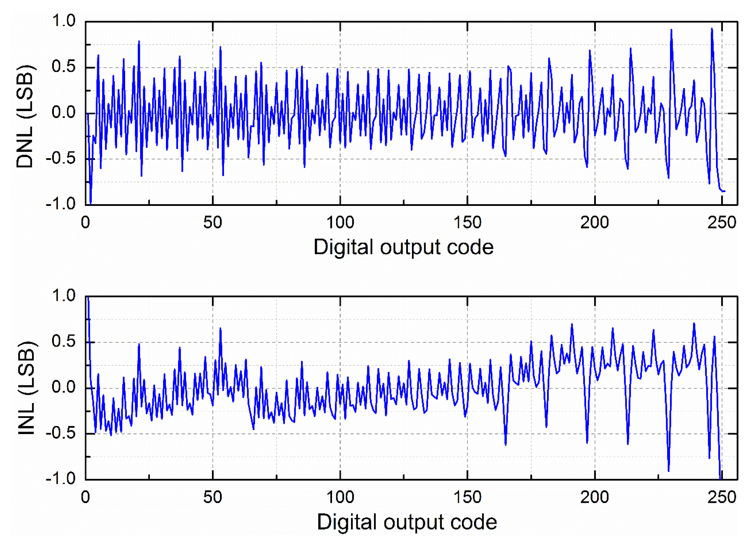
The control logic is used to generate internal asynchronous clocks, register the decision results of the comparators, and control the switching of the CDAC accordingly [20]. Several typical power-efficient switching sequences for CDAC, such as monotonic [22], splitting monotonic [23], and bypass switching techniques, have been proposed to improve the power efficiency. According to the reference [24], it was observed that the bypass method yields better results with less switching activity [25,26,27] because of the basic idea to skip the conversion steps for several significant bits when the signal is within a predefined window. Moreover, the skip operation reduces the error accumulation to improve the static performance. In this design, the CDAC is built with a segmented pre-quantization and bypass switching scheme [28], and the actual differential structure is displayed as single-ended for clarity in Figure 6.
The capacitors array of CDAC is divided into two parts with high and low weight by the switch Smerge. To keep the comparator’s input common-mode voltage constant, each capacitor is split into two identical small capacitors. The input signal is sampled onto the capacitors array via channel-selection-embedded bootstrap switches.
After sampling, all the switches are turned off, and only the low-weight capacitors array is connected to the comparator, equivalent to a 4-bit ADC. The comparator directly performs the first comparison without switching any capacitors to obtain the first digital code D1 [22], which is fed back to switch the minimum capacitor 8C in the high-weight capacitors array, providing an initial voltage. The subsequent digital codes D2–D4 are compared with D1, as Figure 6a shows. If one of the codes is the same as D1, that means the previous output of the CDAC is not enough, so the associated large capacitor is switched, contributing a corresponding weight output to the CDAC. In case the code is different from D1, it indicates that the last output of the CDAC is excessive, and the relevant large capacitor is bypassed, just maintaining the original state without switching. The monotonic procedure is either upward or downward to avoid unnecessary opposite direction switching of high-weight large capacitors, therefore reducing the power consumption and nonlinearity.
Once the high-weight capacitors are properly set, the switch Smerge is turned on, and the two arrays are merged. Meanwhile the low-weight capacitors array is reset to the initial condition. Then, the entire structure is changed back to 8-bit ADC, entering the residual quantization phase for the low 4-bit digital codes D5–D8, as shown in Figure 6b. In the whole conversion process, all quantization is done using the low-weight capacitors array, relaxing the settling constraints of the CDAC.
Ideally, the proportion of 4C in the low-weight capacitors array should be the same as that of 64C in the whole capacitors array, both being 1/2. However, the presence of parasitic capacitance changes the ratio. Since the total capacitance of high-weight capacitors array is much larger than that of low-weight capacitors array, even the same parasitic capacitance will occupy different proportions in different weight capacitor arrays, resulting in gain errors in CDAC output between high 4-bit coarse quantization and low 4-bit global quantization stages, so it is necessary to insert equilibrium capacitor (denoted as CE) to balance the parasitic differences between the two capacitor arrays, as shown below:
C L C L + C P L = C H C H + C P H + C E
CH and CL represent the total capacitance of high and low weight capacitors array, respectively; that is, CH = 64C + 32C + 16C + 8C = 120C, CL = 4C + 2C + C + C = 8C. CPH and CPL represent the parasitic capacitance respectively, which can be obtained from the layout parameters extraction.
In order to further solve the potential wrong conversion caused by inaccurate parameter extraction and manufacturing process variation, a compensation capacitor (denoted as CC) with the weight of 4 is used to provide 1-bit redundancy (corresponding to digital code DC), whose error correction range is up to 4/128 = 3.125%.
The gain error of TI SAR ADC mainly comes from the parasitic effect and capacitance mismatch of CDAC. When selecting a capacitor size, there are two main factors to consider: thermal noise (kT/C) and matching accuracy [9]. A compact and reasonable CDAC layout is deliberately designed by using full-custom metal-oxide-metal (MOM) capacitors [29] with the unit capacitance of 1.5 fF. Benefiting from 1-bit redundancy, intrinsic capacitor matching, and careful layout routing, the gain error can be minimized to a tolerant level [30].

4. Measured Results

The ADC prototype was manufactured in a 55-nm one-poly nine-metal (1P9M) CMOS process with a core area of 400 μm × 550 μm, and a large number of decoupling capacitors were filled inside the chip to keep the power supply voltage clean and stable. The die micrograph is shown in Figure 7. The static performance of differential non-linearity (DNL) and integral non-linearity (INL) is shown in Figure 8. The measured DNL and INL were +0.93/−0.85 LSB and +0.71/−0.91 LSB, respectively.
The output fast Fourier transform (FFT) spectrum is shown in Figure 9 at a 115 MHz input frequency and 2.6 GS/s, with an spurious-free dynamic range (SFDR) of 52.0 dB and signal-to-noise-and-distortion ratio (SNDR) of 41.52 dB. Figure 10 shows SNDR and SFDR versus input frequency at 2.6 GS/s. Within the input frequency range of 500 MHz, the SFDR was greater than 47.9 dB, the SNDR was greater than 38.2 dB, and the effective number of bits (ENOB) was greater than 6-bit. SFDR was above 40.3 dB and SNDR was above 31.8 dB in the first Nyquist zone. However, as the input frequency increased to the Nyquist frequency, the SNDR decreased by about 9 dB, which was much lower than the expected theoretical values. This result reveals that although the proposed method could suppress sample/hold circuit mismatch, the performance was not satisfactory in the high-frequency region due to other non-ideal factors, such as the master clock path mismatch, input signal path mismatch, and so on [5].
Based on the simulation results, the total power consumption of 60 mW at 1.2 V supply voltage was composed as follows: 12 mW for the clock generation module and 48 mW for the SAR ADCs array (that is, 6 mW/slice for every sub-ADC). The FoM calculated within the 500 MHz input frequency was 348 fJ/conversion-step. The performance summary is shown in Table 1.

5. Conclusions

A 2.6 GS/s 8-bit SAR ADC prototype with eight-channel direct sampling TI architecture has been presented. The SNDR was above 38.2 dB up to 500 MHz input frequency and above 31.8 dB up to the Nyquist frequency. The DNL and INL were +0.93/−0.85 LSB and +0.71/−0.91 LSB, respectively. The ADC consumed 60 mW, occupied an area of 400 μm × 550 μm, and realized a FoM of 348 fJ/conversion-step. In general, this design is a beneficial attempt of time-skew, calibration-free technology, which achieves acceptable results in low and medium frequency, and provides a reference for related research and design. If the calibration for time skew is used for future work, better performance can be promised.

Author Contributions

D.W. (Dong Wang) designed the circuits, analyzed the measurement data, and wrote the manuscript. X.Z., J.L., X.G. and L.Z. assisted the circuits implementation and simulation. D.W. (Danyu Wu) and H.L. performed the chip test. J.W. contributed to the technical discussions and reviewed the manuscript. X.L. gave some valuable guidance and confirmed the final version of manuscript.

Funding

This research was supported by National Science and Technology Major Project of China, grant number 2016ZX03001002.

Conflicts of Interest

The authors declare no conflict of interest.

References

  1. Lin, C.; Wei, Y.; Lee, T. A 10-bit 2.6-GS/s Time-Interleaved SAR ADC With a Digital-Mixing Timing-Skew Calibration Technique. IEEE J. Solid-State Circuits 2018, 53, 1508–1517. [Google Scholar] [CrossRef]
  2. Harpe, P.J.A.; Zhou, C.; Bi, Y.; van der Meijis, N.P.; Wang, X.; Philips, K.; Dolmans, G.; de groot, H. A 26µW 8 bit 10 MS/s Asynchronous SAR ADC for Low Energy Radios. IEEE J. Solid-State Circuits 2011, 46, 1585–1595. [Google Scholar] [CrossRef]
  3. Doris, K.; Janssen, E.; Nani, C.; Zanikopoulos, A.; van der Weide, G. A 480 mW 2.6 GS/s 10b Time-Interleaved ADC With 48.5 dB SNDR up to Nyquist in 65 nm CMOS. IEEE J. Solid-State Circuits 2011, 46, 2821–2833. [Google Scholar] [CrossRef]
  4. Fredenburg, J.A.; Flynn, M.P. Statistical Analysis of ENOB and Yield in Binary Weighted ADCs and DACS With Random Element Mismatch. IEEE Trans. Circuits Syst. Regul. Pap. 2012, 59, 1396–1408. [Google Scholar] [CrossRef]
  5. Miki, T.; Ozeki, T.; Naka, J. A 2-GS/s 8-bit Time-Interleaved SAR ADC for Millimeter-Wave Pulsed Radar Baseband SoC. IEEE J. Solid-State Circuits 2017, 52, 2712–2720. [Google Scholar] [CrossRef]
  6. Xu, D.-G.; Pu, J.; Xu, S.-L.; Zhang, Z.-P.; Chen, K.-R.; Chen, Y.-Y.; Zhang, J.-A.; Wang, J.-A. A 10-bit 1.2 GS/s 45 mW time-interleaved SAR ADC with background calibration. IEICE Electron. Express 2018, 15, 1–12. [Google Scholar]
  7. Kull, L.; Pliva, J.; Toifl, T.; Schmatz, M.; Francese, P.A.; Menolfi, C.; Brandli, M.; Kossel, M.; Morf, B.; Andersen, T.M.; et al. Implementation of Low-Power 6–8 b 30–90 GS/s Time-Interleaved ADCs With Optimized Input Bandwidth in 32 nm CMOS. IEEE J. Solid-State Circuits 2016, 51, 636–648. [Google Scholar] [CrossRef]
  8. Stepanovic, D.; Nikolic, B. A 2.8 GS/s 44.6 mW Time-Interleaved ADC Achieving 50.9 dB SNDR and 3 dB Effective Resolution Bandwidth of 1.5 GHz in 65 nm CMOS. IEEE J. Solid-State Circuits 2013, 48, 971–982. [Google Scholar] [CrossRef] [Green Version]
  9. Lee, S.; Chandrakasan, A.P.; Lee, H. A 1 GS/s 10b 18.9 mW Time-Interleaved SAR ADC With Background Timing Skew Calibration. IEEE J. Solid-State Circuits 2014, 49, 2846–2856. [Google Scholar] [CrossRef]
  10. Lee, H.; Aurangozeb; Park, S.; Kim, J. A 6-bit 2.5-GS/s Time-Interleaved Analog-to-Digital Converter Using Resistor-Array Sharing Digital-to-Analog Converter. IEEE Trans. Very Large Scale Integr. VLSI Syst. 2015, 23, 2371–2383. [Google Scholar] [CrossRef]
  11. Wei, H.; Zhang, P.; Sahoo, B.D.; Razavi, B. An 8 Bit 4 GS/s 120 mW CMOS ADC. IEEE J. Solid-State Circuits 2014, 49, 1751–1761. [Google Scholar] [CrossRef]
  12. Zhu, Y.; Chan, C.-H.; Zheng, Z.-H.; Li, C.; Zhong, J.-Y.; Martins, R.P. A 0.19 mm2 10 b 2.3 GS/s 12-Way Time-Interleaved Pipelined-SAR ADC in 65-nm CMOS. IEEE Trans. Circuits Syst. Regul. Pap. 2018, 65, 3606–3616. [Google Scholar] [CrossRef]
  13. Janssen, E.; Doris, K.; Zanikopoulos, A.; Murroni, A.; van der Weide, G.; Lin, Y.; Alvado, L.; Darthenay, F.; Fregeais, Y. An 11b 3.6 GS/s time-interleaved SAR ADC in 65nm CMOS. In Proceedings of the 2013 IEEE International Solid-State Circuits Conference Digest of Technical Papers, San Francisco, CA, USA, 17–21 February 2013; pp. 464–465. [Google Scholar]
  14. Kundu, S.; Alpman, E.; Lu, H.-L.; Lakdawala, H.; Paramesh, J.; Jung, B.; Zur, S.; Gordon, E. A 1.2 V 2.64 GS/s 8 bit 39 mW Skew-Tolerant Time-interleaved SAR ADC in 40 nm Digital LP CMOS for 60 GHz WLAN. IEEE Trans. Circuits Syst. Regul. Pap. 2015, 62, 1929–1939. [Google Scholar] [CrossRef]
  15. Lien, Y.-C. A 14.6 mW 12b 800 MS/s 4×time-interleaved pipelined SAR ADC achieving 60.8 dB SNDR with Nyquist input and sampling timing skew of 60fsrms without calibration. In Proceedings of the 2016 IEEE Symposium on VLSI Circuits (VLSI-Circuits), Honolulu, HI, USA, 15–17 June 2016; pp. 1–2. [Google Scholar]
  16. Zhu, Y.; Chan, C.-H.; U, S.-P.; Martins, R.P. An 11b 900 MS/s time-interleaved sub-ranging pipelined-SAR ADC. In Proceedings of the ESSCIRC 2014—40th European Solid State Circuits Conference (ESSCIRC), Venice Lido, Italy, 22–26 September 2014. [Google Scholar] [CrossRef]
  17. Zhu, X.; Zhou, L.; Wu, D.; Wu, J.; Liu, X. A 6 mW 325 MS/s 8 bit SAR ADC with background offset calibration. IEICE Electron. Express 2017, 14, 1–8. [Google Scholar] [CrossRef]
  18. Kuo, B.-Y.; Chen, B.-W.; Tsai, C.-M. A 0.6 V, 1.3 GHz dynamic comparator with cross-coupled latches. In Proceedings of the VLSI Design, Automation and Test (VLSI-DAT), Hsinchu, Taiwan, 27–29 April 2015; pp. 1–4. [Google Scholar]
  19. Fang, J.; Thirunakkarasu, S.; Yu, X.; Silva-Rivas, F.; Zhang, C.; Singor, F.; Abraham, J. A 5-GS/s 10-b 76-mW Time-Interleaved SAR ADC in 28 nm CMOS. IEEE Trans. Circuits Syst. Regul. Pap. 2017, 64, 1673–1683. [Google Scholar] [CrossRef]
  20. Kull, L.; Toifl, T.; Schmatz, M.; Francese, P.A.; Menolfi, C.; Brandli, M.; Kossel, M.; Morf, T.; Andersen, T.M.; Leblebici, Y. A 3.1 mW 8b 1.2 GS/s Single-Channel Asynchronous SAR ADC With Alternate Comparators for Enhanced Speed in 32 nm Digital SOI CMOS. IEEE J. Solid-State Circuits 2013, 48, 3049–3058. [Google Scholar] [CrossRef]
  21. Chen, S.M.; Brodersen, R.W. A 6-bit 600-MS/s 5.3-mW Asynchronous ADC in 0.13-μm CMOS. IEEE J. Solid-State Circuits 2006, 41, 2669–2680. [Google Scholar] [CrossRef]
  22. Liu, C.-C.; Chang, S.-J.; Huang, G.-Y.; Lin, Y.Z. A 10-bit 50-MS/s SAR ADC With a Monotonic Capacitor Switching Procedure. IEEE J. Solid-State Circuits 2010, 45, 731–740. [Google Scholar] [CrossRef]
  23. Liu, C.-C.; Chang, S.-J.; Huang, G.Y.; Lin, Y.-Z.; Huang, C.-M. A 1V 11fJ/conversion-step 10bit 10MS/s asynchronous SAR ADC in 0.18µm CMOS. In Proceedings of the 2010 Symposium on VLSI Circuits, Honolulu, HI, USA, 15–18 June 2010; pp. 241–242. [Google Scholar]
  24. Santhanalakshmi, M.; Yasoda, K. Verilog-A implementation of energy-efficient SAR ADCs for biomedical application. In Proceedings of the 2015 19th International Symposium on VLSI Design and Test, Ahmedabad, India, 26–29 June 2015; pp. 1–6. [Google Scholar]
  25. Huang, G.-Y.; Chang, S.-J.; Liu, C.-C.; Lin, Y.-Z. A 1-µW 10-bit 200-kS/s SAR ADC With a Bypass Window for Biomedical Applications. IEEE J. Solid-State Circuits 2012, 47, 2783–2795. [Google Scholar] [CrossRef]
  26. Liu, Y.; Yuan, C.; Hung, Y.L.Y. A capacitor constructed bypass window switching scheme for energy-efficient SAR ADC. In Proceedings of the 2014 IEEE International Symposium on Circuits and Systems (ISCAS), Melbourne, VIC, Australia, 15–18 June 2014; pp. 1352–1355. [Google Scholar]
  27. Wang, T.-Y.; Li, H.-Y.; Ma, Z.-Y.; Huang, Y.-J.; Peng, S.-Y. A Bypass-Switching SAR ADC With a Dynamic Proximity Comparator for Biomedical Applications. IEEE J. Solid-State Circuits 2018, 53, 1743–1754. [Google Scholar] [CrossRef]
  28. Wang, X.; Zhou, X.; Li, Q. A High-Speed Energy-Efficient Segmented Prequantize and Bypass DAC for SAR ADCs. IEEE Trans. Circuits Syst. Express Briefs 2015, 62, 756–760. [Google Scholar] [CrossRef]
  29. Abusleme, A.; Dragone, A.; Haller, G.; Murmann, B. Mismatch of lateral field metal-oxide-metal capacitors in 180 nm CMOS process. Electron. Letters 2012, 48, 286–287. [Google Scholar] [CrossRef]
  30. Zhu, Y.; Chan, C.-H.; U, S.-P.; Martins, R.P. An 11b 450 MS/s Three-Way Time-Interleaved Subranging Pipelined-SAR ADC in 65 nm CMOS. IEEE J. Solid-State Circuits 2016, 51, 1223–1234. [Google Scholar] [CrossRef]
Figure 1. Eight-channel time-interleaved (TI) successive approximation register (SAR) analog-to-digital converter (ADC) architecture.
Electronics 08 00305 g001
Figure 2. (a) Multi-phase clock generator (MPCG), (b) D flip-flop (DFF), and (c) timing diagram.
Electronics 08 00305 g002
Figure 3. Channel-selection-embedded bootstrap switch.
Electronics 08 00305 g003
Figure 4. (a) SAR ADC overview, and (b) asynchronous timing diagram.
Electronics 08 00305 g004
Figure 5. The diagram of comparator’s background offset calibration.
Electronics 08 00305 g005
Figure 6. (a) Pre-quantization stage, and (b) global quantization stage in segmented pre-quantization and bypass switching scheme.
Electronics 08 00305 g006
Figure 7. Die micrograph with layout view.
Electronics 08 00305 g007
Figure 8. Measured differential non-linearity (DNL) and integral non-linearity (INL).
Electronics 08 00305 g008
Figure 9. Output fast Fourier transform (FFT) spectrum.
Electronics 08 00305 g009
Figure 10. Signal-to-noise-and-distortion ratio (SNDR) and spurious-free dynamic range (SFDR) versus input frequency.
Electronics 08 00305 g010
Table 1. Performance summary.
Technology55-nm 1P9M CMOS
Architecture8-channel TI SAR
Sampling Rate2.6 GS/s
Resolution8-bit
Power60 mW
Active Area0.22 mm2
DNL+0.93/−0.85 LSB
INL+0.71/−0.91 LSB
SFDR≥50.94 dB (up to115 MHz)
≥47.9 dB (up to 500 MHz)
≥40.3 dB (up to Nyquist)
SNDR≥40.54 dB (up to115 MHz)
≥38.2 dB (up to 500 MHz)
≥31.8 dB (up to Nyquist)
FoM 1348 fJ/conversion-step
Calibration ComplexityOn-chip offset calibration only
1 FoM = Power/(2ENOB × Sampling frequency).

