Abstract
Based on the 0.5 μm GaAs enhancement/depletion (E/D) Pseudomorphic High Electron Mobility Transistor (pHEMT) process, a 7.5–9 GHz two-channel amplitude phase control multi-function chip (MFC) was developed successfully. The chip was integrated with a 6-bit digital phase shifter, a 6-bit digital attenuator, and a single pole single throw (SPST) switch in each channel. A design for the absorptive SPST switch is deployed to optimize the return loss and control channel array calibration. In the 8 dB and 16 dB attenuation bit, a switched-path-type topology is employed in order to obtain a good flatness of attenuation characteristic and achieve low additive phase shift. A 27-bit serial-to-parallel converter (SPC) was introduced to decrease the control lines and pads of the chip, and the power consumption was less than 70 mW. The measurement result shows that the insertion loss is less than −13 dB and the return loss is better than −19 dB. In both channels, the 64-state root mean square (RMS) errors of the phase shifter is less than 2° and the RMS parasitic amplitude error is less than 0.2 dB. The RMS attenuation error is less than 0.45 dB and the RMS parasitic phase error is less than 2.4°. The size of the chip is 3.5 mm × 4.5 mm.
1. Introduction
Phased array technologies have been widely applied to satellite communications and defense systems to implement high-performance radar systems [1]. However, phased array radar systems consist of thousands of T/R modules which increase the systems’ complexity and cost. By integrating several functions such as phase and gain control, driver amplifiers, and switches on a single multi-function chip [2], the sharp problem can be solved. Packing the multi-function chip (MFC) for compact and low cost T/R modules has already been realized in a phased array system [3]. With the development of advanced 3D integration technology, MFC chips are introduced to further improve the integration density of 3D microsystems in space applications [4].
In recent years, several GaAs multi-function chips have been presented, but higher integration implies a large number of control lines and pads to the chips [5,6,7]. By combination of serial-to-parallel converter on-chip, the number of control lines and pads can be substantially reduced [8,9]. Meanwhile, integrating multi-channels on one multi-function chip is beneficial as it decreases the system’s size and cost. With high performance and high integration, the MFC chips must be promising.
According to actual application demand, a 7.5–9 GHz two-channel amplitude–phase control multi-function chip (MFC) was developed successfully via the 0.5 μm GaAs E/D pHEMT process. The variation of amplitude–phase in channel will influence the performance of T/R modules. Therefore, a single pole single throw (SPST) switch was designed to control array calibration, and an absorptive topology was selected to optimize the return loss. In order to achieve extended bandwidth, good attenuation flatness, and low additive phase shift, a switched-path-type topology was employed in 8 dB and 16 dB attenuation bit. It is complex and difficult to assemble the T/R modules due to the existence of numerous pads. A 27-bit serial-to-parallel converter was integrated to decrease the control pads, which also reduces the size and cost of T/R modules. To the best of our knowledge, the insertion loss, phase error, attenuation error, and return loss of the presented MFC represent state-of-art performances.
2. Circuit Design
Based on the 0.5 μm GaAs E/D pHEMT process, a multi-function chip (MFC) is designed; the diagram is shown in Figure 1. The MFC comprises two channels (CH); each one consists of a 6-bit digital phase shifter (PHS), a 6-bit digital attenuator (ATT), and a single pole single throw (SPST) switch. The phase and the amplitude of RF signals are controlled by the PHS and ATT. The on–off state of each channel is chosen by an SPST switch. The 26-bit serial-to-parallel converter (SPC) is needed to control RF Field Effect Transistors (FETs) of the PHS, ATT, and SPST switch in two channels, and another bit is used to output differential voltages to control an off-chip switch. In total, a 27-bit serial-to-parallel converter is designed to decrease the control pads of the chip.
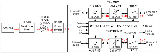
Figure 1.
The diagram of the actual application.
The summary of the link budget analysis is also shown in Figure 1. Based on the demand of the actual application, no additional driver amplifies need to be designed in the MFC. The total gain of the receiving channel is sufficient with the introduction of the Low Noise Amplifer (LNA) at the RF frontend. On the other hand, based on the 0.5 μm GaAs E/D pHEMT process, the noise performance of LNA is no longer competitive, so that the LNA at the RF frontend is not integrated in the MFC and is designed in another process.
2.1. Absorptive SPST Switch Design
In many applications, reflective switches are not suitable due to the significant standing waves introduced between components [10]. In this MFC, an absorptive SPST switch has been designed to control array calibration of channel; the structure is shown in Figure 2. In this design, when VT is 0 V, the SPST switch is in the on-state. A two-stage series-shunt structure is adopted to achieve high isolation performance. When VT is −3 V, the SPST switch is in the off-state. Two 50 Ω absorptive resistors are used to decrease the return loss. A 45 dB isolation and a 19 dB return loss have been achieved in these two ways. The parameters of SPST switch design are shown in Table 1.
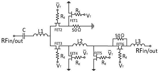
Figure 2.
The structure of the absorptive single pole single throw (SPST) switch.

Table 1.
The parameters of SPST switch design.
2.2. Attenuator Design
The attenuator is comprised of six attenuation bits which contain 64 states. The maximum attenuation is 31.5 dB, in 0.5 dB steps. Figure 3 shows the schematic of the attenuator; the order of 6-bit attenuation is ranked by the performance of input and output return loss. The on-state (0 V) and off-state (−3 V) of each FET is controlled by the gate bias voltage that is provided by the serial-to-parallel converter.
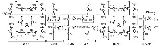
Figure 3.
The schematic of the 6-bit digital attenuator.
In the 0.5 dB and 1 dB attenuation bits, a simplified T-type network with series-FETs topology is used; the topology introduces a low insertion loss. Two dB and 4 dB bits adopt the bridge-T-type structure, which has great terminal matching characteristics. For the large attenuation of the 8 dB and 16 dB bits, parasitic parameters of FETs would bring more additive phase shift and deteriorate the flatness of the attenuation characteristic. Therefore, switch-path-type topology is employed. The required attenuation is obtained by switching the signal between a long micro-strip and a pi-type resistor network. By adjusting the length of the micro-strip between the two paths, the additive phase shift can be decreased. Meanwhile, a good flatness of attenuation is achieved by using two single pole double throw (SPDT) switches, which provide high isolation between the reference and attenuation states.
The parameters of attenuator design are shown in Table 2.
Table 2.
The parameters of attenuator design.
2.3. Phase Shifter Design
The schematic of the 6-bit phase shifter is illustrated in Figure 4. The 6-bit phase shifter provides 64 states in steps of 5.625°, which corresponds to phase shifts of 45°, 5.625°, 11.25°, 22.5°, 90°, and 180°. The major consideration for the order of the 6-bit phase shifter is the input and output characteristic. Each FET’s on-state (0 V) and off-state (−3 V) is controlled by the gate bias voltage, which also is provided by the serial-to-parallel converter.
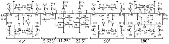
Figure 4.
The schematic of the 6-bit digital phase shifter.
Series FETs filter topology is applied in 5.625° bit, which causes low insertion loss. The bridge-T-type topology is selected for the 11.25° and 22.5° bits. The FETs’ parasitic parameters are absorbed as phase shift element, and the topology has a good phase shift flatness. For the 45°, 90°, and 180° bits, switched filter topology is implemented. Between two SPDT switches, one path is constructed using a high-pass filter network which causes signal phase lead, and the other path is constructed using a low-pass filter network which makes signal phase lag. The necessary phase shift is obtained by switching the signal between the two paths. Although the use of two SPDT switches introduces higher insertion loss compared to other bits, the implementation of high phase shift values using this topology provides a low amplitude imbalance, good match characteristics, and phase shifter flatness.
The parameters of phase shifter design are shown in Table 3.
Table 3.
The parameters of phase shifter design.
2.4. Serial-to-Parallel Converter Design
Based on the 0.5 μm GaAs E/D pHEMT process, which has both enhancement/depletion mode pHEMTs on one substrate, a 27-bit serial-to-parallel converter is designed. The depletion mode (D-mode) pHEMT works as a load to constrain the current, while the enhancement mode (E-mode) pHEMT works as a switch to achieve logic function. In contrast to other logic families (e.g., two-phase dynamic FET logic (TDFL), source-coupled FET logic (SCFL), pseudo-complementary FET logic (PCFL), feedback FET logic (FFL), etc.), the direct-coupled FET logic (DCFL) is the most commonly used logic style and is chosen in this design, which has compact topology and low power dissipation [11].
The circuit structures of NO and NAND are shown respectively in Figure 5a,b, which consists of 1 × 5 μm size E/D-mode pHEMT. Shift and hold registers are composed of a D-flipflop, which contain 4 NAND blocks and 4 NO blocks, as shown in Figure 5c.
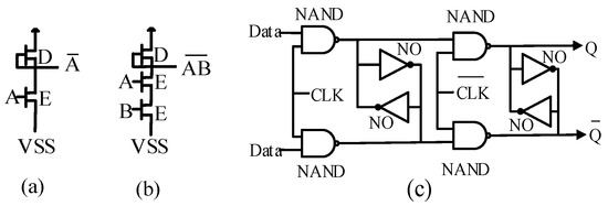
Figure 5.
(a) NO circuit structure, (b) NAND circuit structure, (c) D-flipflop circuit structure.
As shown in Figure 6, the serial-to-parallel converter contains 4 TTL-direct-coupled FET logic (DCFL) level shifters, 27 shift registers, 27 hold registers, and 27 output buffers. The level shifter converts the external TTL signals into internal DCFL signals. The shift registers transform the DATA into binary numbers where the 1-state stands for 0 V while the 0-state is −3 V. The shift registers shift the 0/1-state to next shifter register when CLK falling edge comes. When the LD signal arrives, hold registers receive the parallel data from the shifter register and transmit to the output buffers, which provide differential voltages to RF FETs. The power consumption of the 27-bit serial-to-parallel converter is less than 70 mW, while −5 V and 5 V voltages are supplied. The power consumption ratio of level shifts; output buffers, shift registers, and hold registers are around 1:15:35:35. The serial DATA out bit stream (SDout) is available and can be cascaded to a second chip or be used to check the working state of the serial-to-parallel converter. The integration of the serial-to-parallel converter decreases the number of control pads from 54 to 9.
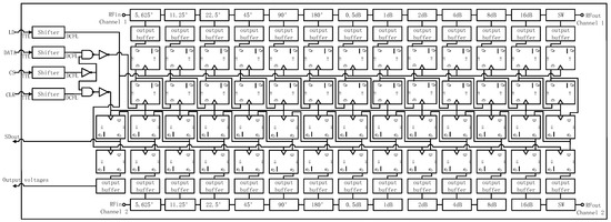
Figure 6.
The schematic of the digital circuit.
3. Measurement Results
Figure 7 shows the photograph of the two-channel multi-function chip which is fabricated by the 0.5 μm GaAs E/D pHEMT process. The chip size is 3.5 mm × 4.5 mm. On-wafer measurements are carried out for the performance characterization. A signal generator (NI-PXI) is employed to provide appropriate digital input waveform with a clock frequency of 10 MHz. The MFC is tested by vector network analyzer (Agilent PNA 5224A, Agilent Technologies Inc., Santa Clara, USA) using Ground-Signal-Ground (GSG) co-planar microwave probes pitch on probe station [12].
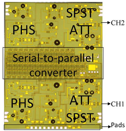
Figure 7.
Photograph of the fabricated multi-function chip.
As shown in Figure 8a,b, the input and output return losses of MFC are more than 19 dB in both channels. The attenuator and phase shifter exhibit good flatness of relative attenuation and relative phase shift, respectively, in the frequency range from 7.5 to 9 GHz (Figure 8c,d). In Figure 8e, measured root mean square (RMS) attenuation error of <0.45 dB and RMS parasitic phase error of <2.4° is shown at all 64 states. Figure 8f shows <2° RMS phase error and <0.2 dB RMS parasitic amplitude error measured for the phase shifter. The trend of measured results are almost in accord with simulated results for ATT and PHS. In Figure 8g, <13 dB insertion loss is achieved, and the difference between measured and simulated results may be caused by process model accuracy.
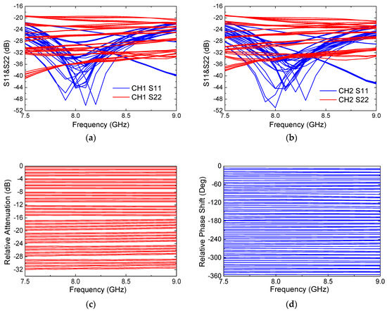
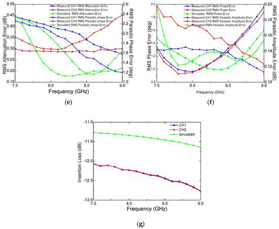
Figure 8.
(a) Measured channel 1 (CH1) input and output return loss of all states, (b) measured channel 2 (CH2) input and output return loss of all states, (c) measured relative attenuation of all states, (d) measured relative phase shift of all states, (e) measured and simulated CH1 and CH2 root mean square (RMS) error of attenuation and parasitic phases, (f) measured and simulated CH1 and CH2 RMS error of phase and parasitic amplitude, (g) measured and simulated CH1 and CH2 insertion loss.
Table 4 summarizes the performance comparison of this work with other published MFCs working in close frequency ranges. Characteristics including insertion loss, RMS phase error, RMS attenuation error, and return loss are better than the previous reported MFCs. This work is also integrated with two channels and a serial-to-parallel converter on a single MFC chip, which has the benefit of decreasing the system’s size and cost. By applying new technologies like the 0.18 μm GaAs E/D pHEMT process, the size of MFC could reach 4 × 3.7 mm2 [8]. However, comparing with the 0.5 μm GaAs E/D pHEMT process, which is commonly used for the MFC designs in X-band, the cost of the 0.18 μm process is much larger. Compared with other published MFCs with the same 0.5 μm process, our design shows higher integration, the size of which is much smaller than the average 4 × 5 mm2 [13]. Furthermore, the 3.5 × 4.5 mm2 size of our MFC successfully approaches the above 4 × 3.7 mm2 fabricated by the new 0.18 μm technology. The frequency band 7.5–9 GHz of the MFC is chosen for a real application of narrow-band data transmission within 8–8.5 GHz.
Table 4.
Performance comparison of relevant multi-function chip (MFC).
4. Conclusions
In this letter, a high-performance 7.5–9 GHz two-channel multi-function chip integrated with a serial-to-parallel converter is presented. A design of the absorptive SPST switch is deployed to optimize the return loss and control channel array calibration. In the 8 dB and 16 dB attenuation bits, a switched-path-type topology is adopted in order to obtain a good flatness of attenuation characteristic and a low additive phase shift. The control pads are reduced from 54 to 9 by integrating the serial-to-parallel converter. The measurement result shows that the two channels of MFC have <13 dB insertion loss at reference state, and >19 dB return loss at all states. An RMS attenuation error of <0.45 dB and an RMS parasitic phase error of >2.4° are obtained for the attenuator. An RMS phase error of <2° and an RMS parasitic amplitude error of <0.2 dB are achieved for the phase shifter. Good return loss, high attenuation, and phase shift accuracy are achieved in this two-channel multi-function chip.
Author Contributions
Methodology, S.Z. (Shancheng Zhou); software, J.Z.; validation, H.Y.; data curation, S.Z. (Shouli Zhou); writing—original draft preparation, S.Z. (Shancheng Zhou); writing—review & editing, Z.W.; supervision, S.Z. (Shouli Zhou); project administration, J.W.; funding acquisition, Z.W.
Funding
This research was funded by the National Natural Science Foundation of China grant number 61604128 and the Fundamental Research Funds for the Central Universities grant number 2017QN81002.
Acknowledgments
The authors would like to thank the Institute of Aerospace Electronics Engineering of Zhejiang University for providing research platform and technical support.
Conflicts of Interest
The authors declare no conflict of interest.
References
- Shin, D.H.; Jeong, J.C.; Moon, S.M.; Yom, I.B. Compact Ku-band GaAs Multifunction Chip for SATCOM Phased Arrays. In Proceedings of the 45th European Microwave Conference (EuMC), Paris, France, 7–10 September 2015; pp. 1471–1474. [Google Scholar]
- Boer, A.D.; Mouthaan, K. GaAs Mixed Signal Multi-Function X-Band MMIC with 7 Bit Phase and Amplitude Control and Integrated Serial to Parallel Converter. In Proceedings of the IEEE 30th European Microwave Conference, Paris, France, 1–4 March 2007. [Google Scholar]
- Yeo, S.K.; Chun, J.H.; Kwon, Y.S. A 3-D X-band T/R module package with an anodize aluminum multilayer substrate for phased array radar applications. IEEE Trans. Adv. Pack. 2010, 33, 883–891. [Google Scholar] [CrossRef]
- Carlofelice, A.D.; Paulis, F.D.; Fina, A.; Marcantonio, U.D.; Orlandi, A.; Tognolatti, P. Compact and reliable T/R Module Prototype for Advanced Space Active Electronically Steerable Antenna in 3-D LTCC Technology. IEEE Trans. Microw. Theory Tech. 2018, 66, 2746–2756. [Google Scholar] [CrossRef]
- Billstrom, N.; Berg, H.; Gabrielson, K.; Hemmendorff, E.; Hertz, M. T/R “core chips” for S-, C-, and, X-band radar systems. In Proceedings of the IEEE 34th European Microwave Conference, Amsterdam, The Netherlands, 12–14 April 2005; pp. 1029–1032. [Google Scholar]
- Vliet, F.E.; Boer, A.D. Fully-Integrated Core chip for X-Band Phased-Array T/R modules. In Proceedings of the IEEE MTT-S International Microwave Symposium Digest, Fort Worth, TX, USA, 6–11 June 2004; pp. 1753–1756. [Google Scholar]
- Xie, Y.Y.; Zhao, Z.R.; Liu, W.J.; Li, Y.P.; Chen, F.X. A Microminiature 7–8.5 GHz GaAs Multi-Function Chip. Micronanoelectronic Technol. 2016, 53, 281–287. [Google Scholar]
- Ciccognani, W.; Ghione, M.; Limiti, E.; Longhi, P.E.; Pirola, M.; Quaglia, R. A Compact High Performance X-Band Core-Chip with on Board Serial-to-Parallel Conversion. In Proceedings of the IEEE 40th European Microwave Conference, Paris, France, 28–30 September 2010; pp. 902–905. [Google Scholar]
- Pirola, M.; Quaglia, R.; Ghione, G.; Ciccognani, W.; Limiti, E. 13-bit GaAs serial-to-parallel converter with compact layout for core-chip applications. Microelectron. J. 2014, 45, 864–869. [Google Scholar] [CrossRef]
- Liao, W.; Tang, G.Q.; Deng, L.; Wu, G.C.; Zhang, Y. Design and Implementation of a Broadband Absorption Type SPDT Switch. Piezoelectrics Acoustooptics 2014, 36, 360–362. [Google Scholar]
- Bentini, A.; Pasciuto, B.; Ciccognani, W.; Limiti, E.; Nanni, A.; Romanini, P. Design and Realization of GaAs Digital Circuit for Mixed Signal MMIC Implementation in AESA Applications. Int. J. Microw. Sci. Technol. 2011, 2011, 387137. [Google Scholar] [CrossRef]
- Wang, K.R.; Wang, Z.Y.; Wang, G.; Chen, H.; Zheng, Q.; Yu, F.X. Design of a low-insertion-phase-shift MMIC attenuator integrated with a serial-to-parallel converter. IEICE Electron. Express 2017, 14, 1–7. [Google Scholar] [CrossRef]
- Jeong, J.C.; Kwak, C.; Yom, I.B.; Seo, I.J.; Jo, I.H. Life test of an X-band MMIC multi-function chip for active phased array radar applications. Microelectron. Reliab. 2015, 55, 815–821. [Google Scholar] [CrossRef]
- Shin, D.; Kim, C.Y.; Kang, D.W.; Rebeiz, G.M. A High-Power Packaged Four-Element X-Band Phased-Array Transmitter in 0.13-μm CMOS for Radar and Communication Systems. IEEE Trans. Microw. Theory Tech. 2013, 61, 3060–3071. [Google Scholar] [CrossRef]
- Sim, S.; Jeon, L.; Kim, J.G. A Compact X-Band Bi-Directional Phased-Array T/R Chipset in 0.13 μm CMOS Technology. IEEE Trans. Microw. Theory Tech. 2013, 61, 562–569. [Google Scholar] [CrossRef]
- Liu, C.; Li, Q.; Li, Y.H.; Deng, X.D.; Li, X.; Liu, H.T.; Xiong, Y.Z. A Fully Integrated X-Band Phased-Array Transceiver in 0.13-μm SiGe BiCMOS Technology. IEEE Trans. Microw. Theory Tech. 2016, 64, 575–583. [Google Scholar] [CrossRef]
- Nguyen, V.V.; Nam, H.; Choe, Y.J.; Lee, B.H.; Park, J.D. An X-band Bi-Directional Transmit/Receive Module for a Phased Array System in 65-nm CMOS. Sensors 2018, 18, 2569. [Google Scholar] [CrossRef] [PubMed]
- Heijningen, M.; Boer, A.; Hoogland, J.A.; Wanum, M.; Hek, A.P.; Vliet, F.E.; Brouzes, H. Multi Function and High Power Amplifier Chipset for X-Band Phased Array Frontends. In Proceedings of the European Microwave Integrated Circuits Conference, Manchester, UK, 10–13 September 2006; pp. 237–240. [Google Scholar]


© 2019 by the authors. Licensee MDPI, Basel, Switzerland. This article is an open access article distributed under the terms and conditions of the Creative Commons Attribution (CC BY) license (http://creativecommons.org/licenses/by/4.0/).