Article

Electric Double Layer Field-Effect Transistors Using Two-Dimensional (2D) Layers of Copper Indium Selenide (CuIn7Se11)

1
Department of Physics, Southern Illinois University Carbondale, Carbondale, IL 62901, USA
2
Department of Materials Science and NanoEngineering, Rice University, Houston, TX 77005, USA
3
Department of Physics and Astronomy, Georgia State University, Atlanta, GA 30303, USA
*
Authors to whom correspondence should be addressed.
Electronics 2019, 8(6), 645; https://doi.org/10.3390/electronics8060645
Submission received: 10 April 2019 / Revised: 28 May 2019 / Accepted: 4 June 2019 / Published: 7 June 2019
(This article belongs to the Special Issue Advanced Technologies in Nanoelectronics)

Abstract

:
Innovations in the design of field-effect transistor (FET) devices will be the key to future application development related to ultrathin and low-power device technologies. In order to boost the current semiconductor device industry, new device architectures based on novel materials and system need to be envisioned. Here we report the fabrication of electric double layer field-effect transistors (EDL-FET) with two-dimensional (2D) layers of copper indium selenide (CuIn7Se11) as the channel material and an ionic liquid electrolyte (1-Butyl-3-methylimidazolium hexafluorophosphate (BMIM-PF6)) as the gate terminal. We found one order of magnitude improvement in the on-off ratio, a five- to six-times increase in the field-effect mobility, and two orders of magnitude in the improvement in the subthreshold swing for ionic liquid gated devices as compared to silicon dioxide (SiO2) back gates. We also show that the performance of EDL-FETs can be enhanced by operating them under dual (top and back) gate conditions. Our investigations suggest that the performance of CuIn7Se11 FETs can be significantly improved when BMIM-PF6 is used as a top gate material (in both single and dual gate geometry) instead of the conventional dielectric layer of the SiO2 gate. These investigations show the potential of 2D material-based EDL-FETs in developing active components of future electronics needed for low-power applications.

1. Introduction

Since the discovery of single Molybdenum Disulphide (MoS2) layer as an active channel component in field-effect transistors (FETs) [1], research on 2D materials for electronics and optoelectronics has gained massive momentum. Over a short period of time, various new classes of 2D materials [2,3], e.g., transition metal dichalcogenides (TMDs), group III-VI layered materials, MXenes, etc., have emerged as potential future candidates for post-silicon electronics. However, most of the work performed on 2D material-based FETs focused on the conventional back gate approach where the use of SiO2 as the gate dielectric is typical. Some of the advantages of SiO2 back gate includes their natural availability, simpler device fabrication, and easier modulation of gate thickness. However, a low dielectric constant of SiO2 (κ = 3.9) results in low capacitances and, therefore, the need for high threshold voltages for device operations [4]. Higher operating voltages imply higher operating cost for integrated circuit chips. High-κ dielectric materials, such as inorganic, polymer, and electrolyte dielectrics, have been incorporated into FETs depending on cost, durability, operation speed, and transconductance for better performance of FETs, as well as potential applications in flexible and stretchable electronics [4,5]. In this regard, ionic liquids have emerged as promising dielectric gate materials in FETs [6,7,8]. Electric double layers (EDL) formed by ionic liquid result in higher capacitance due to their atomically thin charge layer. The charge accumulated (Q) by a capacitor is given by Q = C × V, where C is the capacitance and V is the applied voltage. The higher capacitance in the EDL yield in higher electrostatic charge carrier doping in the semiconductor channel ultimately results in high on-state current and lower threshold and operational voltages. Further, it has been shown through other different applications, such as batteries, capacitors, fuel cells, solar cells, and actuators, that ionic liquids have exceptional and stable chemical properties [8,9,10,11,12].
Recently, ionic liquids have been integrated with two-dimensional (2D) material-based FETs, which has resulted in various fascinating applications [13,14,15,16,17,18,19,20]. For example, studies have indicated that superconductivity can be induced in atomically thin layers of ZrNCl-based FETs at T = 15.2 K by using ionic liquid DEME-TFSI as the gate [13], ambipolar metal-insulator transition can be induced in thin flakes of black phosphorus-based FETs with DEME-TFSI as the gate dielectric [14], and ferromagnetism can be induced in cobalt (Co)-doped titanium dioxide (TiO2) in EDL-FETs with DEME-TFSI as the gate [15]. Lastly, device performance can be substantially improved in few-layered MoS2-based ambipolar FETs, where it was shown that by using DEME-TFSI as the EDL gate, mobilities of ~60 cm2 V−1 s−1 and on-off ratios of ~107 with the subthreshold swing reaching near the ideal value of ≈50 mV/dec [16] can be achieved. Even though 2D materials have shown great potential, a great deal of investigation needs to be carried out to match the performance of silicon-based devices. So far binary 2D materials, such as MoS2, WSe2, InSe, In2Se3, etc. have been the main focus of investigations [21,22,23]. Lately, however, multi-component derivatives (via doping or alloying) and heterostructures of this binary compounds have attracted attention due to tunable electronic properties [24,25]. Bulk copper indium selenide (CIS) has been widely used in optoelectronics research and industry as a new-generation material for ultra-thin flexible solar cells due to its high photoresponsivity and wide spectral range [26]. When the copper-to-indium ratio lies between 1:5 and 1:9, CIS forms a γ-phase with hexagonal stacking of close-packed selenium anions, thus yielding a layered structure [26]. Such a layered structure, therefore, can be exfoliated into ultra-thin conductive channel materials (not possible for extensively investigated thin films). For example, a 2D-layered structure of ternary copper indium selenide (CIS)—specifically, CuIn7Se11 (γ-phase of CIS)—has shown to have excellent electronic and optoelectronic properties with field-effect mobility reaching ~37 cm2 V−1 s−1 along with photo-responsivity of ~32 A W−1 and a response time ~9 μs [27,28]. However, most of these materials are investigated in the light of FET-based devices with conventional SiO2 gates.
Here, we show that by constructing an electric double layer field-effect transistor (EDL-FET) using CuIn7Se11 as the channel material and an ionic liquid electrolyte (1-butyl-3-methylimidazolium hexafluorophosphate (BMIM-PF6)) as the gate terminal can provide FET devices with further tunability. The reason for choosing BMIM-PF6 is as follows: It has been shown that mobility (μ) is higher for BMIM-PF6-based FETs compared to other ionic liquids [29]. Our investigations show that field-effect mobility of μFE ≈ 21.84 cm2 V−1 s−1 can be achieved with a BMIM-PF6 ionic liquid top gate which is a 5.4 times improvement from the corresponding value μFE ≈ 4.04 cm2 V−1 s−1 of the same device with a conventional SiO2 back gate. One order of magnitude increase in the on-off ratio > 104 with the ionic liquid gate as compared to the SiO2 gate was also observed. We further demonstrate two orders of magnitude improvement in the subthreshold swing with a subthreshold swing (SS) of ~0.3 V/dec with the ionic liquid gate (which was ~9.6 V/dec with the SiO2 gate). Although ionic liquids (IL) show improved device performances, water absorption by the IL degrades performance over time and mechanical properties of the liquid restrict their utilization for practical application [4]. Such drawbacks can be avoided by using ionic gel polymers. Ion-gel overcomes these issues by incorporating/physical cross-linking ionic liquid in a block of the polymer [4]. Ion-gel combines ion mobility of IL with mechanically stable solid films of the polymer [4]. Therefore, we investigated FET performance with an ion-gel (BMIM-PF6/PEO) top gate (on a different device) which shows an improvement in the performance with the ion-gel gate (μFE ≈ 0.42 cm2 V−1 s−1, on/off ratio ~ 103, and SS ~ 0.81 V/dev) compared to the SiO2 gate (μFE of 0.23 cm2 V−1 s−1, on/off ratio of ~100, and SS of 107 V/dev). We also show that device parameters (for example, the field effect mobility) can be further improved by operating the device in a dual gate mode (with BMIM-PF6/PEO as a top gate and SiO2 as a back gate).

2. Materials and Methods

A detailed synthesis of CuIn7Se11 has been reported elsewhere [27]. In a nutshell, single crystals of CuIn7Se11 were grown via a typical melting and recrystallization process with Cu2Se and In2Se3 as precursors. The mixture in a 1:7 ratio (Cu2Se:In2Se3) was ground in a mortar and transferred to a quartz ampoule (at a pressure of < 10−3 torr along with argon flushing). The ampoule was heated in a furnace at 950 ℃ for five hours followed by slow cooling to 700 ℃ and natural cooling thereafter. An optical image of the as-synthesized single crystal of CuIn7Se11 (black mica-like texture) is shown in the inset of Figure 1a. The energy-dispersive X-ray spectrum of the CuIn7Se11 flake is shown in Figure 1a and it indicates Cu:In:Se in a 1:7:11 ratio. The strong peak at 1.74 keV corresponds to the underlying silicon substrate. Detailed structural characterization (SEM, HRTEM, EDX and XRD) revealed the two-dimensional layers of CuIn7Se11 [27,28].
Using Scotch tape-assisted mechanical exfoliation, a few layers of CuIn7Se11 flakes were exfoliated from the as-grown crystals on SiO2/Si substrate with a 1000 nm SiO2 layer. Surface roughness (root mean square) of the exfoliated flake was found to be 0.2 nm. As-exfoliated flakes were contacted via chromium, Cr (~20 nm, deposition rate ~ 0.009–0.011 nm/s) and gold, Au (~200 nm, deposition rate ~ 0.13–0.22 nm/s), and deposited by using a shadow mask in a home-built thermal evaporation system. The low deposition rate rules out the possibility of burning channel layers. An optical image of the flake which contacts with the Au/Cr pads is shown in the inset of Figure 1c. As contacted flakes were transferred on the chip holder (CSB02842, Spectrum Semiconductor, San Jose, CA, USA) and gold wire was used to connect chip holder pins to the metal contacts. The exfoliated flakes and the as-fabricated devices were not treated with any other technique, such as annealing, before measurements. The chip holder was mounted on the cold head of the cryostat (RDK-101D, SHI Cryogenics Group, Elk Grove Village (Chicago), IL, USA). Four terminal (source, drain, back gate, and top gate) FET measurements were performed using Keithley 2400-series source meters. The underlying SiO2 was used as the back gate terminal. A small and continuous drop of 1-butyl-3-methylimidazolium hexafluorophosphate (BMIM-PF6, CAS No.: 174501-64-5, ACROS Organics, Geel, Belgium) was used as the top gate terminal. The electronic measurements with an ionic liquid top gate that are reported here were taken once the drain current in the device was stabilized (typically 5–7 days). For ionic liquid-based gel polymer electrolyte, we have used poly (ethylene oxide) (PEO, average Mv 100,000, CAS No.: 25322-68-3, Sigma-Aldrich, St. Louis, MO, USA) as a polymer matrix. A monomer of poly (ethylene oxide) was self-assembled into a physically cross-linked network with BMIM-PF6 to form an ion-gel electrolyte. Ion-gel was prepared by mixing BMIM-PF6 (10% by weight) and PEO (90% by weight) in methanol (as a solvent) and the mixture was heated to 50 ℃ before drop casting a small drop of the mixture onto the device.

3. Results and Discussion

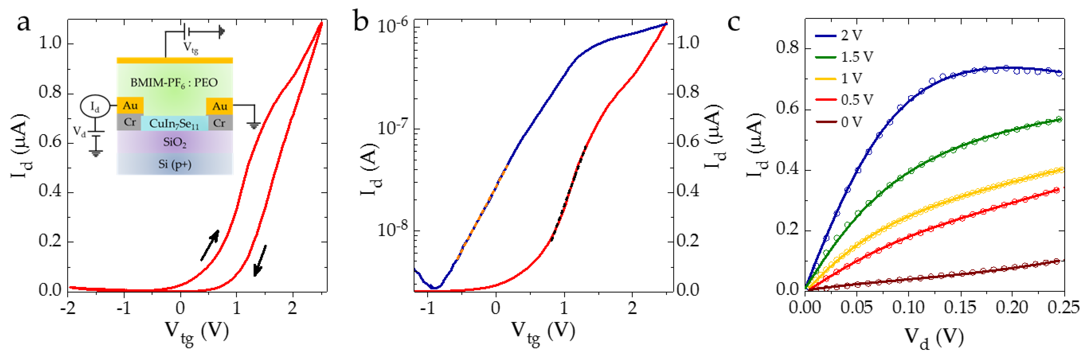
3.1. Electronic Transport with Dielectric Gate

Electronic transport measurements of CuIn7Se11 FET (Device I) using dielectric (SiO2) as the back gate are shown in Figure 1. Figure 1b shows transfer characteristics (drain current Id vs. gate voltage Vg) between a gate voltage of −60 V and +60 V and at a constant drain voltage of Vd = 1 V. A typical n-type behavior was observed and it indicates the In-rich nature of the semiconducting channel. On-set voltage was found to be Von ~ −15 V, which differentiates from the on-state of the FET from the off-state of the FET. Hysteresis was observed with the cycling of the back gate voltage, which indicates charge trapping at the CuIn7Se11 and SiO2 interface and/or defects/trap states in the conduction channel. The figure of merit associated with FETs were calculated using the forward cycle of transfer characteristics, as shown in Figure 1c. In the off-state of FET (Vbg < −20 V), the drain current was found to be Ioff ~ 0.5–0.7 nA. As the gate voltage is increased, the channel starts conducting (on-state) and the maximum drain current was observed to be Ion ~ 353 nA at Vbg = 60 V. Thus, the on-off ratio was estimated to be ~103. Field-effect mobility is the average drift speed of charge carriers under a unit electric field. Field-effect mobility (μFE) was estimated from Equation (1):
μ FE = L W   C g   V d   I d V bg
where L ~ 10 μm and W ~ 9 μm corresponds to the length and the width of the device, respectively. The oxide capacitance (Cox = 3.45 × 10⁻⁹ F cm−2) was calculated by using the formula Cox = ε0 × εr/dox, where, εr = 3.9 and dox = 1000 nm are the relative permittivity and thickness of the SiO2, respectively. Transconductance, gm = ∂Id/∂Vbg ~ 1.06 × 10⁻⁸ S, was calculated for +40 V ≤ Vbg ≤ +60 V and it is shown by a black dashed line in Figure 1c. Field-effect mobility was estimated to be μFE ≈ 4.04 cm2 V−1 s−1. This estimated mobility is almost order of magnitude lower than previously reported values for CuIn7Se11 FET [28], which might be due to the difference in channel thickness, as seen previously in other 2D materials [30,31,32]. These values of mobilities are comparable with other Se-based FETs, In2Se3FE ~ 30 cm2 V−1 s−1) [33], In2Se3FE ~ 2.5 cm2 V−1 s−1) [34], InSe (μFE ~ 0.1 cm2 V−1 s−1) [35], InSe (μFE ~ 32.6 cm2 V−1 s−1) [36], GaSe (μFE ~ 0.1 cm2 V−1 s−1) [37], and WSe2FE ~ 80 cm2 V−1 s−1) [23].
The subthreshold swing is the gate voltage required for increasing drain current by an order of magnitude in the subthreshold region. Subthreshold swing (SS) was calculated using Equation (2):
SS = ( | log ( I d ) V g | max ) 1
The subthreshold slope (∂log(Id)/∂Vg) was calculated in the subthreshold region by plotting the transfer curve in the semi-log scale (blue curve in Figure 1c) and it is shown by the yellow dashed line in Figure 1c. SS was estimated to be 9.6 V/dec and it is a substantially different from the ideal SS (~ 60 mV/dec). This deviation could be due to either a depletion layer formed due to trap states [38] and/or higher thickness (1000 nm) of the SiO2 layer. SS, field-effect mobility, and other device parameters are closely related quantities and they are governed by the capacitance of the FET [39]. A further understanding of device performance is needed, however, such analysis will not add to the core findings of the current article. We plan to perform the analysis presented in [39] in our future work.
Output characteristic (drain current Id vs. drain voltage Vd) under different gate voltages (0 V ≤ Vbg ≤ +60 V) is shown in Figure 1d. Output characteristics show an almost linear current-voltage response for low voltage bias, known as the linear region. Linear current-voltage response implies ohmic-like contacts and barrier effects can be neglected. As the drain voltage is increased, the FET goes into saturation mode and it behaves as the constant current source which can be used for voltage amplification. As seen from Figure 1d, applied back gate voltage determines the level of constant current through the channel. It has to be noted that the drain current in output characteristics (~ 2.9 nA at Vd = 1 V and Vg = 60 V) is significantly lower than the drain current in transfer characteristics (~ 353 nA at Vd = 1 V and Vg = 60 V). This could be due to the transient nature of the drain current in the presence of constant applied gate voltage, as seen previously in MoS2 FETs [40].

3.2. Electronic Transport with an Electric Double Layer Gate

Electronic transport measurements of CuIn7Se11 FET (Device I) using an electric double layer (BMIM-PF6) as the top gate are shown in Figure 2. Transfer characteristics with the electric double layer gate are shown in Figure 2a. Similar to back gate transport, n-type conduction was observed with Von ~ 0.8 V. Off-state Id was found to ~1–2 nA, whereas the on-state Id was found to be ~57 μA at Vtg = +3 V. Thus, the on/off ratio was estimated to be >104, which shows one order of magnitude improvement from the corresponding value of the back gate (~103). Using Equation (1), mobility was estimated to be μFE ≈ 21.84 cm2 V−1 s−1 where gm ~ 4.47 × 10⁻⁵ S (black dashed line in Figure 2b), was calculated for 2 V ≤ Vtg ≤ 3 V. Here we have used Cg ~ 2.5 μF cm−2, estimated from the Mott-Schottky method (discussed later in this section). Mobility shows an almost 5.4 times improvement from the corresponding value of the back gate. It is crucial to estimate the EDL capacitance at the electrolyte-semiconductor interface as capacitance is found to vary with the interface. The capacitance of the EDL depends on ionic liquid-semiconductor interface.For example, the capacitance of DEME-TFSI was found to vary as CEDL ≈ 9.2 μF cm−2 for ZrNCl [13], CEDL ≈ 7.2 μF cm−2 (electron) and ≈ 4.7 μF cm−2 (hole) for MoS2 [41], CEDL ≈ 34 μF cm−2 for ZnO [42] and CEDL ≈ 20 μF cm−2 for VO2 [43]. Several techniques have been used to estimate capacitance directly at the ionic liquid-semiconductor interface. For example, electrochemical impedance spectroscopy (EIS) was used in a ZnO thin film transistor [44], Hall-effect measurement was used in MoS2 thin flake transistors [41], the interconnection between an SiO2 back gate and ionic liquid top gate (change in threshold voltage of EDL-FET with application of back gate voltage) in dual gating FET [16] and the Mott-Schottky method was used for organometal perovskite solar cells [45]. We have used the Mott-Schottky method to estimate the EDL capacitance which we used for the mobility calculation.
Ionic liquid (BMIM-PF6) forms a different type of EDL with a gold pad and CuIn7Se11. A schematic of two different EDL capacitances (C1 with BMIM-PF6: CuIn7Se11 and C2 with BMIM-PF6: Au) is shown in the Figure 2c. These capacitors are connected in parallel and the total capacitance of the IL will be the sum of the individual capacitance, Ctot = ΣCi. For the Mott-Schottky method, source and drain terminals were connected together (shorted) to form a single electrode. Using the Mott-Schottky method, (1/CIL)2 was estimated as a function of voltage. A plot of CIL as a function of voltage is shown in Figure 2d. Total capacitance was found not to vary a great deal as a function of the voltage and its value is Ctot ~ 25 μF cm−2. EDL capacitance of BMIM-PF6: Au has been previously reported as C2 ~ 7.5 μF cm−2 [46]. Thus, EDL capacitance of BMIM-PF6: CuIn7Se11 can be estimated as C1 ~ 2.5 μF cm−2. Our estimated value of capacitance is comparable with the previously reported capacitance of BMIM-PF6: semiconductor interface [29]. We have used this value of capacitance to evaluate the performance of electric double layer gated FETs.
The subthreshold swing was improved by two orders of magnitude, SS ~ 0.3 V/dec (yellow dashed line in Figure 2b), which indicates the lower number of trap states for the EDL gate compared to trap states for the dielectric gate. The subthreshold swing of a FET device can be given by Equation (3) [47]:
SS = ln ( 10 )   k   T e   ( 1 + C d C ox )
where e is an electronic charge, k is Boltzmann’s constant, T is the temperature, Cd is the depletion layer capacitance and Cox is the oxide capacitance. A minimum limit of SS (~60 mV/dec at T = 300 K) can be found by letting Cd/Cox → 0. Physically, it means the effect of the depletion layer formed by the p-n junction is minimum/negligible. We believe that the two orders of change in SS seen in our device imply that Cd/Cox is lower for the ionic top gate compared to that of the SiO2 back gate. This is further evident in reduced hysteresis upon cycling of the top gate voltage, indicating lower trap states at the BMIM-PF6-CuIn7Se11 interface compared to trap states at the CuIn7Se11-SiO2 interface. Further, it is to be noted that SS does not match with the ideal SS and this could be due to a depletion layer formed by bulk trap states originating from defeats in the channel, as well as interface trap states at the BMIM-PF6-CuIn7Se11 interface. Improved performance of the FET by the EDL gate could be due to many reasons: lower interface traps and/or higher electrostatic doping and/or reduction in the Schottky barrier thickness due to the ultra-thin dielectric [16]. The figures of merit from the back gate FET and top gate FET are summarized in Table 1.
Output characteristics under different top gate voltages (0 V ≤ Vtg ≤ +3 V) are shown in Figure 2e. Linear current-voltage at low voltage bias (linear region) was observed as seen in the back gate characteristics. As voltage is increased, the current becomes constant as the FET goes into the saturation region. It is to be noted that the contact current in the saturation region is rather in obvious with EDL gate than dielectric gate (Figure 2e vs. Figure 1d). Similar to dielectric gate, the drain current in output characteristics is significantly lower than the drain current in transfer characteristics owing to the transient nature of the drain current in the presence of constant applied gate voltage [40].
Similar improvement in the performance of the FET was also observed in another device (Device II) and it is summarized in Table 1. For Device II, a negligible hysteresis was observed, which indicated a almost trap-free BMIM-PF6-CuIn7Se11 interface. Output characteristics and transfer characteristics with the dielectric gate indicate similar device performance as that of Device I. For the dielectric gate, the figures of merit were estimated to be μFE ~ 2.66 cm2 V−1 s−1, on/off ratio ~ 102, SS ~ 29.8 V/dev. Output characteristics and transfer characteristics with the electric double layer gate show an improvement in performance. For the electric double layer gate, the figures of merit were estimated to be μFE ~ 17.73 cm2 V−1 s−1, on/off ratio ~ 103, SS ~ 0.19 V/dev. Mobility shows an almost 6.6 times improvement for the top gate (17.73 cm2 V−1 s−1) as compared to the corresponding value for the back gate (2.66 cm2 V−1 s−1). Similarly, improvement in the subthreshold swing, as well as on/off ratio, was seen for the top gate.

3.3. Electronic Transport with Ion-Gel Gate

As a potential application of the EDL-FET in the solid-state flexible device, we have used an ionic liquid based gel polymer electrolyte as a gate. Performance of the FET with an SiO2 back gate estimates the figures of merit to be μFE of 0.23 cm2 V−1 s−1, on/off ratio of ~100, and SS of 107 V/dev. This performance of Device III was orders of magnitude lower than the other device presented owing to the bulk nature of the channel. It has been previously reported in the case of MoS2 that the mobility of 2D FETs decreases drastically with channel thickness [30,31,32]. Figure 3 shows the electronic transport of CuIn7Se11 FET (Device III) with the ion-gel gate.
Figure 3a shows the transfer characteristics for the ion-gel top gate. Higher hysteresis was observed owing to the rough interface between the semiconductor channel and the polymer gate. The forward cycle in the linear scale (red) and semi-log scale (blue) of the transfer characteristics are shown in Figure 3b. Figures of merit were estimated to be μFE ~ 0.42 cm2 V−1 s−1, on/off ratio ~ 103, and SS ~ 0.81 V/dev. Gate capacitance was estimated to be Cg ≈ 3.36 μF cm−2 by interconnection between the back gate and the top gate, as discussed in following section. Mobility shows an almost 1.8 times improvement from the corresponding value of the back gate. Mobility for the top gate can be further improved upon the application of back gate voltage. Figure 3c shows the output characteristics under different ion-gel top gate voltages (0 V ≤ Vtg ≤ +2 V) which shows a linear region for low voltage bias and a saturation region for high voltage bias.

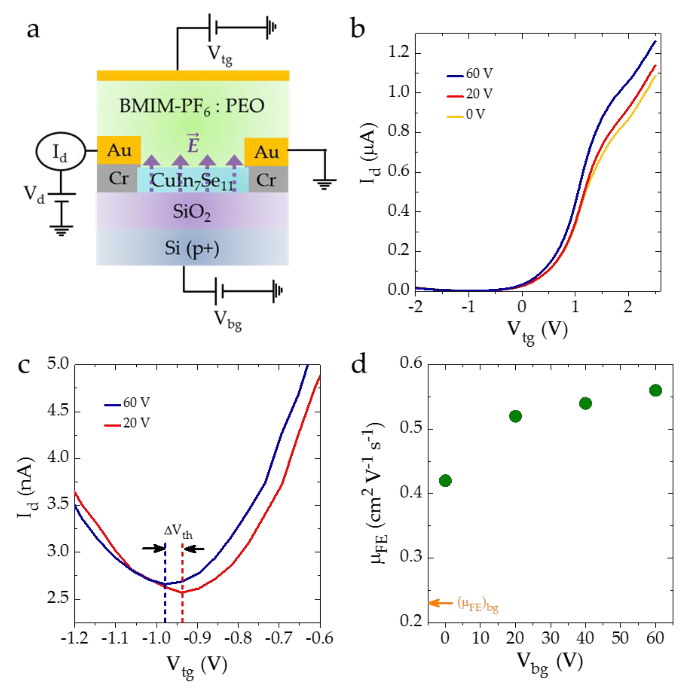
3.4. Electronic Transport with a Dual Gate

Multiple gates in FETs can lead to versatility in the application where properties due to one gate can be modulated by other gates [48,49,50]. Several past investigations have shown that a great level of tunability in device properties can be achieved through a top and bottom dual gate geometry [16,51,52]. For example, an investigation of bilayer graphene with dual (top and bottom) gating indicates an opening of the band gap as well as improvement in general electronic transport behavior due to the screening of disorder potential [52]. In order to test such effects for CuIn7Se11 FETs, we investigated one such device in dual gate operation mode with a SiO2 dielectric back gate and a BMIM-PF6: PEO ion-gel top gate. Figure 4a shows the schematic of a dual gate FET. Figure 4b shows forward cycle of transfer characteristics for the ion-gel top gate with different back gate voltages. It is to be noted that the on-state current was increased upon application of the back gate voltage. Particularly, on-state Id at Vtg = +2.5 V was increased from ~1.08 μA at Vbg = 0 V to ~1.26 μA at Vbg = 60 V which is an almost 1.16 times increase. Dual gating enables an estimation of EDL capacitance of ion-gel by interconnection between the SiO2 back gate and the ion-gel top gate [16]. In dual gating FETs, the application of back gate voltage will change the threshold voltage of the top gate [16]. EDL capacitance was estimated from the change in the threshold voltage (ΔVth) in response to the change in the back gate voltage (ΔVbg) by using Equation (4) [16]:
C tg = Δ V bg Δ V th × C bg
where Cbg = 3.45 × 10⁻⁹ F cm−2 is SiO2 back gate capacitance. For ΔVbg = 40 V, ΔVth was observed to be ~41 mV (Figure 4c), which corresponds to Ctg ≈ 3.36 μF cm−2. The estimated capacitance is higher than the capacitance of IL-based EDL capacitance in the previous section. This could be due to the different dielectric nature of PEO compared to BMIM-PF6 or geometrically different EDL formation. This value of capacitance is used to evaluate the performance of the ion-gel gated FET.
Field-effect mobility due to the ion-gel gate as a function of the back gate voltage is shown in Figure 4d. Mobility, μFE, was found to be 0.56 cm2 V−1 s−1 in the dual gate configuration with constant Vbg = 60 V. Mobility shows an almost 2.4 times improvement from the corresponding value of the back gate. An increase in mobility could be due to an increase in the charge carrier density and/or additional electric field which results in the increased screening of disorder potentials [52]. Dual gating with the ion-gel and the dielectric gate opens the door for tunable and stable performance of a flexible FET.

4. Conclusions

In conclusion, EDL-FETs were fabricated using a few layers of layered CuIn7Se11 flakes. We have successfully incorporated the ionic liquid BMIM-PF6 as a top gate in FETs and the performance was found to be improved compared to that of SiO2 as a back gate. Hysteresis in the transfer characteristics was found to be significantly lower when BMIM-PF6 is used as a top gate, thus indicating lower charge trap states at the CuIn7Se11 and BMIM-PF6 interface. Several parameters that define transistor performance, such as field effect mobility, on-off ratio, and subthreshold swing, were calculated and a comparison between dielectric and electric double-layer gates was demonstrated. The investigation presented here indicated CuIn7Se11 as a potential candidate for the future electronic and optoelectronic industry.

Author Contributions

P.D.P., S.G., M.W. and S.T. conceptualized the experimental protocols; S.L., R.V. and P.M.A. synthesized the samples; S.L. and R.V. provided characterization; P.D.P., S.G. and M.W. fabricated the devices and performed the measurements; P.D.P., S.G. and S.T. analyzed the data. All the authors discussed and co-wrote the manuscript.

Funding

This work was supported by the U.S. Army Research Office MURI grant number W911NF-11-1-0362. S.T. and P.D.P. acknowledges the support from Indo-U.S. Virtual Networked Joint Center Project on “Light Induced Energy Technologies: Utilizing Promising 2D Nanomaterials (LITE UP 2D)” through the grant number IUSSTF/JC-071/2017.

Acknowledgments

ChemDraw (PerkinElmer Informatics, http://www.perkinelmer.com/category/chemdraw) was used to draw the chemical structure of BMIM-PF6 (inset of Figure 2a). We would like to thank Gajanan C. Kulkarni for assisting with ChemDraw.

Conflicts of Interest

The authors declare no conflict of interest. The funders had no role in the design of the study; in the collection, analyses, or interpretation of data; in the writing of the manuscript, or in the decision to publish the results.

References

  1. Radisavljevic, B.; Radenovic, A.; Brivio, J.; Giacometti, V.; Kis, A. Single-layer MoS2 transistors. Nat. Nanotechnol. 2011, 6, 147–150. [Google Scholar] [CrossRef] [PubMed]
  2. Miró, P.; Audiffred, M.; Heine, T. An atlas of two-dimensional materials. Chem. Soc. Rev. 2014, 43, 6537–6554. [Google Scholar] [CrossRef] [PubMed]
  3. Wasala, M.; Sirikumara, H.I.; Raj Sapkota, Y.; Hofer, S.; Mazumdar, D.; Jayasekera, T.; Talapatra, S. Recent advances in investigations of the electronic and optoelectronic properties of group III, IV, and V selenide based binary layered compounds. J. Mater. Chem. C 2017, 5, 11214–11225. [Google Scholar] [CrossRef]
  4. Wang, B.; Huang, W.; Chi, L.; Al-Hashimi, M.; Marks, T.J.; Facchetti, A. High-k Gate Dielectrics for Emerging Flexible and Stretchable Electronics. Chem. Rev. 2018, 118, 5690–5754. [Google Scholar] [CrossRef] [PubMed]
  5. Ye, M.; Zhang, D.; Yap, Y.K. Recent Advances in Electronic and Optoelectronic Devices Based on Two-Dimensional Transition Metal Dichalcogenides. Electronics 2017, 6, 43. [Google Scholar] [Green Version]
  6. Du, H.; Lin, X.; Xu, Z.; Chu, D. Electric double-layer transistors: A review of recent progress. J. Mater. Sci. 2015, 50, 5641–5673. [Google Scholar] [CrossRef]
  7. Wang, D.; Noël, V.; Piro, B. Electrolytic Gated Organic Field-Effect Transistors for Application in Biosensors—A Review. Electronics 2016, 5, 9. [Google Scholar] [CrossRef]
  8. Fujimoto, T.; Awaga, K. Electric-double-layer field-effect transistors with ionic liquids. Phys. Chem. Chem. Phys. 2013, 15, 8983–9006. [Google Scholar] [CrossRef]
  9. Armand, M.; Endres, F.; MacFarlane, D.R.; Ohno, H.; Scrosati, B. Ionic-liquid materials for the electrochemical challenges of the future. Nat. Mater. 2009, 8, 621. [Google Scholar] [CrossRef]
  10. Watanabe, M.; Thomas, M.L.; Zhang, S.; Ueno, K.; Yasuda, T.; Dokko, K. Application of Ionic Liquids to Energy Storage and Conversion Materials and Devices. Chem. Rev. 2017, 117, 7190–7239. [Google Scholar] [CrossRef] [Green Version]
  11. Bisri, S.Z.; Shimizu, S.; Nakano, M.; Iwasa, Y. Endeavor of Iontronics: From Fundamentals to Applications of Ion-Controlled Electronics. Adv. Mater. 2017, 29, 1607054. [Google Scholar] [CrossRef] [PubMed]
  12. Huffstutler, J.D.; Wasala, M.; Richie, J.; Barron, J.; Winchester, A.; Ghosh, S.; Yang, C.; Xu, W.; Song, L.; Kar, S.; et al. High Performance Graphene-Based Electrochemical Double Layer Capacitors Using 1-Butyl-1-methylpyrrolidinium tris (pentafluoroethyl) trifluorophosphate Ionic Liquid as an Electrolyte. Electronics 2018, 7, 229. [Google Scholar] [CrossRef]
  13. Ye, J.T.; Inoue, S.; Kobayashi, K.; Kasahara, Y.; Yuan, H.T.; Shimotani, H.; Iwasa, Y. Liquid-gated interface superconductivity on an atomically flat film. Nat. Mater. 2009, 9, 125–128. [Google Scholar] [CrossRef] [PubMed]
  14. Saito, Y.; Iwasa, Y. Ambipolar Insulator-to-Metal Transition in Black Phosphorus by Ionic-Liquid Gating. ACS Nano 2015, 9, 3192–3198. [Google Scholar] [CrossRef] [PubMed] [Green Version]
  15. Yamada, Y.; Ueno, K.; Fukumura, T.; Yuan, H.T.; Shimotani, H.; Iwasa, Y.; Gu, L.; Tsukimoto, S.; Ikuhara, Y.; Kawasaki, M. Electrically Induced Ferromagnetism at Room Temperature in Cobalt-Doped Titanium Dioxide. Science 2011, 332, 1065–1067. [Google Scholar] [CrossRef] [PubMed]
  16. Perera, M.M.; Lin, M.-W.; Chuang, H.-J.; Chamlagain, B.P.; Wang, C.; Tan, X.; Cheng, M.M.-C.; Tománek, D.; Zhou, Z. Improved Carrier Mobility in Few-Layer MoS2 Field-Effect Transistors with Ionic-Liquid Gating. ACS Nano 2013, 7, 4449–4458. [Google Scholar] [CrossRef] [PubMed]
  17. Jo, S.; Costanzo, D.; Berger, H.; Morpurgo, A.F. Electrostatically Induced Superconductivity at the Surface of WS2. Nano Lett. 2015, 15, 1197–1202. [Google Scholar] [CrossRef]
  18. Lu, J.M.; Zheliuk, O.; Leermakers, I.; Yuan, N.F.Q.; Zeitler, U.; Law, K.T.; Ye, J.T. Evidence for two-dimensional Ising superconductivity in gated MoS2. Science 2015, 350, 1353–1357. [Google Scholar] [CrossRef]
  19. Lu, J.; Zheliuk, O.; Chen, Q.; Leermakers, I.; Hussey, N.E.; Zeitler, U.; Ye, J. Full superconducting dome of strong Ising protection in gated monolayer WS2. Proc. Natl. Acad. Sci. USA 2018, 115, 3551–3556. [Google Scholar] [CrossRef]
  20. Saito, Y.; Nojima, T.; Iwasa, Y. Highly crystalline 2D superconductors. Nat. Rev. Mater. 2016, 2, 16094. [Google Scholar] [CrossRef] [Green Version]
  21. Schwierz, F.; Pezoldt, J.; Granzner, R. Two-dimensional materials and their prospects in transistor electronics. Nanoscale 2015, 7, 8261–8283. [Google Scholar] [CrossRef] [PubMed] [Green Version]
  22. Li, S.-L.; Tsukagoshi, K.; Orgiu, E.; Samorì, P. Charge transport and mobility engineering in two-dimensional transition metal chalcogenide semiconductors. Chem. Soc. Rev. 2016, 45, 118–151. [Google Scholar] [CrossRef] [PubMed]
  23. Ghosh, S.; Wasala, M.; Pradhan, N.R.; Rhodes, D.; Patil, P.D.; Fralaide, M.; Xin, Y.; McGill, S.A.; Balicas, L.; Talapatra, S. Low temperature photoconductivity of few layer p-type tungsten diselenide (WSe2) field-effect transistors (FETs). Nanotechnology 2018, 29, 484002. [Google Scholar] [CrossRef] [PubMed]
  24. Lin, Z.; McCreary, A.; Briggs, N.; Subramanian, S.; Zhang, K.; Sun, Y.; Li, X.; Borys, N.J.; Yuan, H.; Fullerton-Shirey, S.K.; et al. 2D materials advances: From large scale synthesis and controlled heterostructures to improved characterization techniques, defects and applications. 2D Mater. 2016, 3, 042001. [Google Scholar] [CrossRef]
  25. Wang, L.; Hu, P.; Long, Y.; Liu, Z.; He, X. Recent advances in ternary two-dimensional materials: Synthesis, properties and applications. J. Mater. Chem. A 2017, 5, 22855–22876. [Google Scholar] [CrossRef]
  26. Stanbery, B.J. Copper Indium Selenides and Related Materials for Photovoltaic Devices. Crit. Rev. Solid State Mater. Sci. 2002, 27, 73–117. [Google Scholar] [CrossRef]
  27. Lei, S.; Sobhani, A.; Wen, F.; George, A.; Wang, Q.; Huang, Y.; Dong, P.; Li, B.; Najmaei, S.; Bellah, J.; et al. Ternary CuIn7Se11: Towards Ultra-Thin Layered Photodetectors and Photovoltaic Devices. Adv. Mater. 2014, 26, 7666–7672. [Google Scholar] [CrossRef] [PubMed]
  28. Ghosh, S.; Patil, P.D.; Wasala, M.; Lei, S.; Nolander, A.; Sivakumar, P.; Vajtai, R.; Ajayan, P.; Talapatra, S. Fast photoresponse and high detectivity in copper indium selenide (CuIn7Se11) phototransistors. 2D Mater. 2017, 5, 015001. [Google Scholar] [CrossRef]
  29. Fujimoto, T.; Matsushita, M.M.; Awaga, K. Ionic-Liquid Component Dependence of Carrier Injection and Mobility for Electric-Double-Layer Organic Thin-Film Transistors. J. Phys. Chem. C 2012, 116, 5240–5245. [Google Scholar] [CrossRef]
  30. Das, S.; Chen, H.-Y.; Penumatcha, A.V.; Appenzeller, J. High Performance Multilayer MoS2 Transistors with Scandium Contacts. Nano Lett. 2013, 13, 100–105. [Google Scholar] [CrossRef]
  31. Lin, M.-W.; Kravchenko, I.I.; Fowlkes, J.; Li, X.; Puretzky, A.A.; Rouleau, C.M.; Geohegan, D.B.; Xiao, K. Thickness-dependent charge transport in few-layer MoS2 field-effect transistors. Nanotechnology 2016, 27, 165203. [Google Scholar] [CrossRef] [PubMed]
  32. Li, S.-L.; Wakabayashi, K.; Xu, Y.; Nakaharai, S.; Komatsu, K.; Li, W.-W.; Lin, Y.-F.; Aparecido-Ferreira, A.; Tsukagoshi, K. Thickness-Dependent Interfacial Coulomb Scattering in Atomically Thin Field-Effect Transistors. Nano Lett. 2013, 13, 3546–3552. [Google Scholar] [CrossRef] [PubMed] [Green Version]
  33. Island, J.O.; Blanter, S.I.; Buscema, M.; van der Zant, H.S.J.; Castellanos-Gomez, A. Gate Controlled Photocurrent Generation Mechanisms in High-Gain In2Se3 Phototransistors. Nano Lett. 2015, 15, 7853–7858. [Google Scholar] [CrossRef] [PubMed]
  34. Zhou, J.; Zeng, Q.; Lv, D.; Sun, L.; Niu, L.; Fu, W.; Liu, F.; Shen, Z.; Jin, C.; Liu, Z. Controlled Synthesis of High-Quality Monolayered α-In2Se3 via Physical Vapor Deposition. Nano Lett. 2015, 15, 6400–6405. [Google Scholar] [CrossRef] [PubMed]
  35. Tamalampudi, S.R.; Lu, Y.-Y.; Kumar, U.R.; Sankar, R.; Liao, C.-D.; Moorthy, B.K.; Cheng, C.-H.; Chou, F.C.; Chen, Y.-T. High Performance and Bendable Few-Layered InSe Photodetectors with Broad Spectral Response. Nano Lett. 2014, 14, 2800–2806. [Google Scholar] [CrossRef] [PubMed]
  36. Feng, W.; Wu, J.-B.; Li, X.; Zheng, W.; Zhou, X.; Xiao, K.; Cao, W.; Yang, B.; Idrobo, J.-C.; Basile, L.; et al. Ultrahigh photo-responsivity and detectivity in multilayer InSe nanosheets phototransistors with broadband response. J. Mater. Chem. C 2015, 3, 7022–7028. [Google Scholar] [CrossRef]
  37. Yang, S.; Yue, Q.; Cai, H.; Wu, K.; Jiang, C.; Tongay, S. Highly efficient gas molecule-tunable few-layer GaSe phototransistors. J. Mater. Chem. C 2016, 4, 248–253. [Google Scholar] [CrossRef]
  38. Kalb, W.L.; Batlogg, B. Calculating the trap density of states in organic field-effect transistors from experiment: A comparison of different methods. Phys. Rev. B 2010, 81, 035327. [Google Scholar] [CrossRef]
  39. Zebrev, G.I.; Melnik, E.V.; Tselykovskiy, A.A. Interface Traps in Graphene Field-Effect Devices: Extraction Methods and Influence on Characteristics. In Graphene Science Handbook: Size-Dependent Properties; Aliofkhazraei, M., Ali, N., Milne, W.I., Ozkan, C., Mitura, S.S., Gervasoni, J.L., Eds.; CRC Press: Boca Raton, FL, USA, 2016; Volume 5, p. 14. [Google Scholar]
  40. Late, D.J.; Liu, B.; Matte, H.R.; Dravid, V.P.; Rao, C.N. Hysteresis in Single-Layer MoS2 Field Effect Transistors. ACS Nano 2012, 6, 5635–5641. [Google Scholar] [CrossRef]
  41. Zhang, Y.; Ye, J.; Matsuhashi, Y.; Iwasa, Y. Ambipolar MoS2 Thin Flake Transistors. Nano Lett. 2012, 12, 1136–1140. [Google Scholar] [CrossRef]
  42. Yuan, H.; Shimotani, H.; Tsukazaki, A.; Ohtomo, A.; Kawasaki, M.; Iwasa, Y. High-Density Carrier Accumulation in ZnO Field-Effect Transistors Gated by Electric Double Layers of Ionic Liquids. Adv. Funct. Mater. 2009, 19, 1046–1053. [Google Scholar] [CrossRef]
  43. Zhou, Y.; Ramanathan, S. Relaxation dynamics of ionic liquid—VO2 interfaces and influence in electric double-layer transistors. J. Appl. Phys. 2012, 111, 084508. [Google Scholar] [CrossRef]
  44. Singh, M.; Manoli, K.; Tiwari, A.; Ligonzo, T.; Di Franco, C.; Cioffi, N.; Palazzo, G.; Scamarcio, G.; Torsi, L. The double layer capacitance of ionic liquids for electrolyte gating of ZnO thin film transistors and effect of gate electrodes. J. Mater. Chem. C 2017, 5, 3509–3518. [Google Scholar] [CrossRef]
  45. Almora, O.; Aranda, C.; Mas-Marzá, E.; Garcia-Belmonte, G. On Mott–Schottky analysis interpretation of capacitance measurements in organometal perovskite solar cells. Appl. Phys. Lett. 2016, 109, 173903. [Google Scholar] [CrossRef]
  46. Lockett, V.; Horne, M.; Sedev, R.; Rodopoulos, T.; Ralston, J. Differential capacitance of the double layer at the electrode/ionic liquids interface. Phys. Chem. Chem. Phys. 2010, 12, 12499–12512. [Google Scholar] [CrossRef] [PubMed]
  47. Sze, S.M.; Ng, K.K. Physics of Semiconductor Devices; John Wiley & Sons: Hoboken, NJ, USA, 2007. [Google Scholar]
  48. Kim, S.; Nah, J.; Jo, I.; Shahrjerdi, D.; Colombo, L.; Yao, Z.; Tutuc, E.; Banerjee, S.K. Realization of a high mobility dual-gated graphene field-effect transistor with Al2O3 dielectric. Appl. Phys. Lett. 2009, 94, 062107. [Google Scholar] [CrossRef]
  49. Hwang, B.-W.; Yeom, H.-I.; Kim, D.; Kim, C.-K.; Lee, D.; Choi, Y.-K. Enhanced transconductance in a double-gate graphene field-effect transistor. Solid-State Electron. 2018, 141, 65–68. [Google Scholar] [CrossRef]
  50. Zhu, W.; Low, T.; Farmer, D.B.; Jenkins, K.; Ek, B.; Avouris, P. Effect of dual gate control on the alternating current performance of graphene radio frequency device. J. Appl. Phys. 2013, 114, 044307. [Google Scholar] [CrossRef]
  51. Lee, G.-H.; Cui, X.; Kim, Y.D.; Arefe, G.; Zhang, X.; Lee, C.-H.; Ye, F.; Watanabe, K.; Taniguchi, T.; Kim, P.; et al. Highly Stable, Dual-Gated MoS2 Transistors Encapsulated by Hexagonal Boron Nitride with Gate-Controllable Contact, Resistance, and Threshold Voltage. ACS Nano 2015, 9, 7019–7026. [Google Scholar] [CrossRef]
  52. Miyazaki, H.; Tsukagoshi, K.; Kanda, A.; Otani, M.; Okada, S. Influence of Disorder on Conductance in Bilayer Graphene under Perpendicular Electric Field. Nano Lett. 2010, 10, 3888–3892. [Google Scholar] [CrossRef] [Green Version]
Figure 1. Structural characterization of CuIn7Se11 and electronic transport of a CuIn7Se11 FET with a dielectric gate (Device I): (a) Energy-dispersive X-ray spectrum of CuIn7Se11 flake indicating Cu:In:Se in a 1:7:11 ratio where red, green and blue lines correspond to copper, indium and selenium, respectively; Inset: optical image of bulk crystal with scale bar as 1 mm; (b) Transfer characteristics with a dielectric gate for forward cycle and reverse cycle; Inset: schematic of FET; (c) Transfer characteristics with a dielectric gate for forward cycle in the linear scale (red) and semi-log scale (blue); Inset: optical image of typical device (Device II) with scale bar as 10 μm; and (d) output characteristics under different back gate voltages (0 V ≤ Vbg ≤ +60 V) are shown.
Electronics 08 00645 g001
Figure 2. Electronic transport of CuIn7Se11 FET with an electric double layer gate (Device I): (a) Transfer characteristics with an electric double layer gate for the forward cycle and the reverse cycle using the top gate. Inset: chemical structure of ionic liquid (BMIM-PF6); (b) Transfer characteristics with an electric double layer gate for the forward cycle in the linear scale (red) and semi-log scale (blue); (c) A schematic of the EDL-FET and capacitances formed inside the ionic liquid; (d) Total capacitance, Ctot, plotted as a function of applied voltage at 1 kHz frequency as estimated from Mott-Schottky analysis. The shaded area represents the values used for extracting the mobility; (e) Output characteristics under different top gate voltages (0 V ≤ Vtg ≤ +3 V) are shown.
Electronics 08 00645 g002
Figure 3. Electronic transport of the CuIn7Se11 FET with the ion-gel gate (Device III): (a) Transfer characteristics for forward cycle and reverse cycle using the ion-gel top gate, inset: schematic of the EDL-FET; (b) Transfer characteristics with ion-gel gate for forward cycle in the linear scale (red) and semi-log scale (blue); and (c) output characteristics under different top gate voltages (0 V ≤ Vtg ≤ +2 V) are shown.
Electronics 08 00645 g003
Figure 4. Electronic transport of a CuIn7Se11 FET with a dual gate (Device III): (a) Schematic of the FET with a dual (dielectric and ion-gel) gate, arrows indicate the electric field induced in the dielectric gate; (b) Transfer characteristics for the forward cycle with the ion-gel gate under different back gate voltages; (c) Change in threshold voltage of the ion-gel gate with the application of back gate voltage; and (d) field-effect mobility for the top gate FET under different back gate voltages.
Electronics 08 00645 g004
Table 1. Key parameters of CuIn7Se11-based electric double layer field-effect transistors (EDL-FET). Here, Vd = 1 V (Device I) and Vd = 0.1 V (Device II and III), SiO2 thickness = 1000 nm, Vd: Drain-source voltage, μFE: Field-effect mobility, SS: Subthreshold swing, BG: Back gate (dielectric, SiO2), TG: Top gate (electric double layer, BMIM-PF6).
Device #μFE (cm2 V−1 s−1)SS (V/dec)on/off ratio
BGTGBGTGBGTG
Device I4.0421.849.60.30~103~104
Device II2.6617.7329.80.19~102~104
Device III0.230.421070.81~100~103
A device with ion-gel electrolyte using BMIM-PF6 and PEO at top gate.

