Article

HoneyComb ROS: A 6 × 6 Non-Blocking Optical Switch with Optimized Reconfiguration for ONoCs

1
College of Electronic and Information Engineering, Nanjing University of Aeronautics and Astronautics, Nanjing 211100, China
2
School of Electrical and Electronic Engineering, Anhui Science and Technology University, Chuzhou 233100, China
*
Author to whom correspondence should be addressed.
Electronics 2019, 8(8), 844; https://doi.org/10.3390/electronics8080844
Submission received: 30 May 2019 / Revised: 21 July 2019 / Accepted: 26 July 2019 / Published: 29 July 2019
(This article belongs to the Section Microelectronics)

Abstract

:
Silicon photonics has become a commonly used paradigm for on-chip interconnects to meet the requirements of higher bandwidth in computationally intensive applications for manycore processors. Design of an optical switch is a vital aspect while constructing an optical NoC topology which influences the performance of network. We present a HoneyComb optimized reconfigurable optical switch (HCROS), a 6 × 6 non-blocking optical switch where optimized reconfiguration of optical links utilizing the states of basic 2 × 2 optical switching elements (OSE) was achieved while keeping the input-output (I/O) interconnection intact. The proposed 6-port HCROS architecture was further optimized to reduce the number of OSEs to minimize overall power consumption. We proposed a generic algorithm to find the optimal switching combination of OSEs for a particular I/O link to minimize the insertion loss and power consumption. In comparison to other non-blocking architectures, a maximum of 66% reduction in OSEs was observed for the optimized HCROS, which consumes only 12 OSEs. Simulations were performed for all 720 I/O links in different configurations to evaluate the power consumption and insertion loss. We observed up to 92% power savings in the case of optimized HCROS as compared to un-optimized HCROS, and a 79% minimization in insertion loss was also reported as a result of optimization.

1. Introduction

With the advent of the manycore era, hundreds to thousands of cores are expected to be fabricated on a single die for various applications, including the internet of things (IoT), machine learning, and high performance computing where higher bandwidth requirements are highly anticipated in the near future [1,2,3]. The network-on-chip (NoC) effectively exploits the parallelism to provide higher bandwidth demands for future manycore processors [4]. However, the future requirements for the above-mentioned applications cannot be fulfilled using conventional on-chip electrical interconnects [5,6]. The International Technology Roadmap for Semiconductors (ITRS) has acknowledged ONoCs as a substitute to overcome the limitations of traditional on-chip interconnects [7]. Silicon photonics can deliver higher on-chip communication bandwidth by exploiting wavelength division multiplexing (WDM) with lower latency and power consumption, and can achieve a bandwidth of terabits per second (Tbps) [8,9,10].
Optical switches/routers are one of the important building blocks of optical NoCs (ONoC). In the past few years a lot of research has been carried out in regard to designing power and loss efficient optical switch/router architectures [11,12,13,14,15,16,17,18]. An optical switch/router can be designed using different switching fabrics, e.g., a micro-ring resonator (MR) [19] or a Mach-Zehnder switch (MZ) [20] as the basic switching element. Designing optical switch architecture with an optimum number of OSE can minimize overall insertion loss and power consumption in the network topology [21]. Numerous methodologies have been proposed to construct optical switch/router topologies with optimal arrangements of OSEs and different methods have been proposed to optimize the number of OSEs to improve overall network performance [22,23,24,25,26]. In this regard, several multi-stage blocking, strictly non-blocking (SNB), and rearrangeable non-blocking (RNB) optical switch architectures have been presented [27,28], e.g., Benes [29], Spanke-Benes [30], cross switch matrix [31] and Path Independent Loss (PILOSS) [32]. Different ONoC topologies, e.g., mesh, torus, clos and fat tree use 4-port or 5-port optical routers with one core attached to each router. A topology that has two cores attached to a single router has been proposed to form a cluster [33,34]. Cluster-based topology saves chip area and requires a 6-port optical router for the additional core connected to the same router. Different 6-port optical switch/router designs have been proposed to fulfill the requirements of cluster Mesh ONoCs [35,36,37].
The design of an optical switch/router with reduced number of OSEs delivers the advantages of low power consumption and minimized area usage [36]. Power consumption and the inherent feature of insertion loss (IL) in ONoCs require special design considerations for switch design. Reduction in the number of OSEs or MRs in the design of the optical switch can decrease overall IL and power consumption of the optical switch topology, which can improve the overall performance of NoC. In order to minimize the number of OSEs, we need to optimize the switch architecture and identify the optimal configuration in which system peak performance of NoC can be realized. This can be achieved through optimized reconfiguration (here reconfiguration is the switching states of OSE, i.e., active or inactive) of OSEs with the least number of OSEs in an active state where the effects of power consumption and IL are minimal. Designing a non-blocking optical switch with a minimal number of OSEs, and identifying the optimal switching configuration in which the optical switch consumes minimal power with optimal IL is a challenging task. Optimized reconfiguration of optimal switching combinations of OSEs in optical switch topology is the main objective of this article.
Keeping in mind the above-mentioned challenges, we propose an optimized 6-port reconfigurable non-blocking optical switch that consumes only 12 OSEs in an optimized structure with minimized IL and power consumption in an optimal arrangement of OSEs. We exploit the optimal switching combinations of OSEs to reconfigure the switching states to achieve improved performance of the optical switch. In order to achieve the optimum condition of OSEs, we propose an algorithm to find the best switching combination for a desired I/O link with minimal OSEs in an active state. Salient features of the proposed work are as follows:
  • We propose a 6 × 6 reconfigurable non-blocking optical switch with a reduced number of OSE where routing combinations can be reconfigured using optimized reconfiguration to route any desired I/O link.
  • We present a generic algorithm to find the optimal switching combination with the minimal number of OSE in an active, i.e., drop/bar state, which is used to complete the process of optimized reconfiguration to minimize the IL and power consumption. We identify a particular switching combination, where all OSEs are found in an inactive state that leads to minimum power consumption through optimized reconfiguration of the proposed HCROS.
  • Further optimization significantly reduces the number of OSEs in comparison to other non-blocking switch architectures, which leads to minimized hardware cost and compact foot print of the HCROS topology while keeping the non-blocking feature intact.
  • A comprehensive analysis for power consumption and insertion loss for all N! possible I/O links is also discussed in this article.
This paper is structured as follows: Section 2 provides a brief background about multistage optical switch design and its mathematical modeling. Section 3 presents the 6 × 6 HCROS architecture and routing details in both optimized and un-optimized form. A mathematical proof for the non-blocking property is provided in Section 4. An algorithm to find the optimal switching combination of HCROS is provided in Section 5. Comparisons, simulation results and detailed performance analysis are discussed in Section 6. Finally, Section 7 concludes the article with a discussion of intended future work. We will use the following definitions in this article for the terms optimized, optimal, and optimized reconfiguration.
  • Optimized: We use the term “optimized” for the 6-port HCROS optical switch with reduced OSEs as a result of optimization where some OSEs are replaced with waveguide crossings.
  • Optimal: We defined the term “optimal” as the configuration for the minimum number of OSEs in a bar/drop state or more specifically, “optimal switching combination”. Since basic 2 × 2 micro-ring (MR)-based OSE consumes more power in a bar/drop state than in a cross/through state, also the insertion loss of 2 × 2 MR-based OSE is higher in a bar/drop state.
  • “Optimized reconfiguration” is defined as a process of utilizing optimal switching combination (optimal state) to reconfigure OSEs in HCROS to reduce power consumption and minimize insertion loss while ensuring the input to output interconnections are unaffected.
In addition, we use the following definitions to describe the following terms:
  • I/O link: An I/O links is defined as a set of particular “routing combinations” to connect the desired input to output.
  • Routing combination: A routing combination consists of six optical paths to connect each input port to every output port for mapping a particular I/O link, hence it is responsible for transmission of data in parallel.
  • The switching combination is the state of OSEs for a particular routing combination to map a particular I/O link.

2. Background

In this section, we briefly review the basics of the 2 × 2 optical switching element used in the design of an optical switch/router, the transfer matrix-based mathematical model of 2 × 2 basic OSE, and the non-blocking properties of optical switch/routers. MR is widely used as a basic component in optical interconnects due to its compact size and compatibility with CMOS. The functionality of 2 × 2 MR based OSE is illustrated in Figure 1a,b, where 2 × 2 OSE consists of two crossing waveguides and two MRs [19,38]. When the resonant frequency of MR is not the same as the modulated signal, the optical signal simply passes through the waveguide intersection. However, when the wavelength, i.e., λi = λr, the optical signal gets coupled into MR and changes its direction to its respective output [39,40] where λi is the input wavelength while λr is the wavelength of the particular MR, as shown in Figure 1. It consists of two states (1) active state, i.e., drop/bar, and (2) inactive state, i.e., through/cross. In the active state, MRs are in a resonance condition with respective inputs, therefore, input signals I1 and I2 get coupled into upper and lower MRs, respectively, and as a result, I1 and I2 are propagated to O1 and O2, respectively, as shown in Figure 1a. During the inactive state, input signals I1 and I2 pass through using the same waveguide and are transmitted to O2 and O1 as shown in Figure 1b [19]. Detailed I/O mapping of 2 × 2 OSE is shown in Table 1. In this article, we use a MR-based 2 × 2 OSE as the basic design unit for the proposed HCROS architecture and we use the terms drop (DB) and through (TC) for the active and inactive states, respectively.
Basic 2 × 2 OSEs can be used to construct non-blocking multi-stage switch topologies. Basic 2 × 2 OSE denoted by EDs|Ts can be modeled as transfer matrix using the following Equations (1) and (2) where ETs and EDs represent OSE in through and drop states, respectively.
E T S = [ 0 1 1 0 ]
E D S = [ 1 0 0 1 ]
E D S | T S =   E D S   o r   E T S
EDs|Ts is expressed as particular OSE in through (ETs) or drop (EDs) states and is represented as Equation (3). Multistage architecture with N inputs-outputs is represented in the form of a transfer matrix M with S number of stages, where each stage is represented in the form of a block diagonal matrix Ω. Each stage may consist of a straight waveguide, crossing waveguide, OSE in drop (EDs) or through (ETs) states [25]. Straight waveguide is represented with the value of ‘1’ in the transfer matrix. I/O mapping is expressed as O = M.I, where I and O are the input and output column vectors of radix N switch. Transfer matrix M is represented as the product of ΩS matrices, and the proposed HCROS architecture consists of 7 stages where S = (1, 2, … 7) and M is expressed as Equation (4) [25].
M = Ω 1 Ω 2 Ω S 1 Ω S = i = 1 S Ω i
The following set of rules should be followed while designing non-blocking optical switch topology:
  • Input signal from any input In should be routed to any output port On of the radix N optical switch.
  • The link between any input In and output On pair should not block other input-output optical links in particular routing combinations of the radix N optical switch.
  • For an N port non-blocking optical switch there exists N! switching states. For example, N = 6, it contains 6! = 720 possible switching states. For any switch to be non-blocking it should have N! routing states that remain intact, otherwise it would become blocking.

3. Switch Architecture

In this section, the proposed HCROS architecture is discussed in detail including the routing table for both the un-optimized and optimized forms.

3.1. Six-Port Non-Blocking Reconfigurable Optical Switch Architecture

Our proposed HCROS design consists of 6 input and 6 output ports with 15 2 × 2 MR based OSEs, i.e., SE1, SE2, … SE15 and 6 waveguide crossings as shown in Figure 2. The switch can route 6! = 720 switching states. The proposed switch is divided into 7 stages shown in Figure 2 as Ω1, Ω2, Ω3, Ω4, Ω5, Ω6 and Ω7 having 2 × 2 OSEs, and 2 stages with waveguide crossings shown as PI and PO. PI and PO provide the symmetry across both sides of the switch architecture. The architecture presented in Figure 2 looks like a honey comb structure, based on this we named the proposed optical switch, the HoneyComb reconfigurable optical switch (HCROS).
Using the methodology discussed in Section 2, we formulated the stage matrices of HCROS with the help of the expression shown in Equation (5).
Ω S = [ E D S | T S 0 0 0 0 0 E D S | T S 0 0 0 0 0 0 0 0 0 0 E D S | T S 0 0 0 0 0 E D S | T S ] ,   W h e r e   ( S = 1 , 2 , 3 , ...7 )
The complete transfer matrix is written in the form of the following Equation (6)
M = Ω 1 Ω 2 Ω 3 P I Ω 4 P O Ω 5 Ω 6 Ω 7
PI and PO represent stages without OSEs, these two stages are a combination of straight and crossing waveguides and are represented using Equations (7) and (8), respectively. PI is a column permutation matrix while PO is a row permutation matrix.
P I = [ 1 3 5 2 4 6 ] T
P O = [ 1 3 5 2 4 6 ]
Six I/O ports exploit 15 OSEs that can be reconfigured according to the desired routing combination. Table 2 lists six routing combinations for different I/O links denoted as SC1, SC2, … SC6, where links from SC1, SC2, … SC5 cover N(N-1) links. There are a total 6! = 720 distinct I/O links with different routing combinations for the 6-port optical switch, however, the selected 6 routing combinations cover all 30 optical links that can route every input to each output except loopback. We also included a loopback SC6 as the 6th I/O link with a certain routing combination, as shown in Table 2. The remaining routing combinations are just different permutations of these 6 routing combinations [36,41]. For N = 6, I/O links can route a total of 30 links from input to output ports. Using these routing combinations, we reconfigured 15 OSEs, i.e., SE1, SE2, … SE15 to map different I/O links, as listed in Table 2. However, our analysis is not restricted to only these six I/O links, in addition, we have provided a comprehensive performance analysis for all 720 I/O links in Section 6.
Table 3 lists the 15 OSEs used for each routing combination to route an input to a particular output and shows the switching state of each OSE, i.e., drop (DB) or through (TC). For example, I1 can complete its route to every output O1, O2, … O6 in 6 I/O links using routing combinations. Similarly, each input covers a route to every output in the defined 6 I/O links. Note that there are more than one switching combination for each routing combination.
As an example, the switching combination for the SC6 I/O link is shown in Figure 3, where we can observe that I1 → O1, shown in green, uses 5 OSEs to reach output port O1 and all OSEs remain in a drop state. Similarly, other routing combinations are distinguished in separate colors. For one I/O link there could be several possible paths, however for simplicity we have shown all switches in drop states that route one-to-one I/O mapping. Here, we can see that all routing combinations can route their data packets to their respective destination in parallel. The proposed HCROS is a non-blocking architecture and the optimized HCROS falls in the category of RNB (rearrangeable non-blocking) since all input-output combinations of the optical switch are rearranged in a particular manner, such that all the information is transmitted simultaneously [42,43]. A network is said to be RNB when it can incorporate the new I/O link by rearranging some of the switching combinations using the existing OSEs [43]. More details about non-blocking properties and RNB are discussed in Section 4, where a mathematical theorem is provided to proof the non-blocking property of the N×N port switch network.
In Figure 3, it can be seen that all 6 inputs are transmitted to a particular output in parallel depending on the switching states of the OSEs shown in different colors.

3.2. Optimized 6-Port Non-Blocking Reconfigurable Optical Switch Architecture

The proposed HCROS architecture was optimized and a certain number of OSEs were reduced [25]. By reducing the number of OSEs we can achieve a more compact footprint for the optical switch and a reduction in OSEs also minimizes the power consumption and IL caused due to the drop/bar state of OSEs, which consume more power in the drop/bar state than the through/cross state [38]. However, this reduction in OSEs count can lead to a decrease in some routing choices that can deteriorate the performance for some applications. As a result of optimization, we eliminated 3 OSEs in total, the 2 OSEs labeled as SE1, SE2 in the left half and SE11 in the right half of the proposed HCROS architecture. The optimized architecture of optical switch is shown in Figure 4, where we can observe that after optimization, the total OSE count is 12 labelled as SE1, SE2, … SE12. However, the number of waveguide crossings has increased from 6 to 9. A detailed performance analysis of both the un-optimized and optimized designs is discussed in Section 6.
The resulting transfer matrix for the optimized HCROS is expressed in Equation (9).
M = R I Ω 1 Ω 2 P I Ω 3 P O Ω 4 Ω 5 Ω 6
where RI, PI and PO represent stages without OSEs and consist of straight and cross waveguides. The vectors PI/PO define the column/row permutations of the N × N identity matrix and are given by Equations (7) and (8), respectively.
One of the possible switching combinations for optimized HCROS architecture is listed in Table 4. The switching combination of 12 OSEs for 6 I/O links including the straight/crossing waveguides are shown. Reduction in total OSEs still maps all 720 combinations including 6 I/O links SC1, SC2, …. SC6 using the reconfiguration of OSEs.
As an example of optimized HCROS architecture we have shown the SC6 I/O link’s routing combinations in Figure 5. All optical paths are highlighted in separate colors.
The number of active stages, i.e., having OSEs, in the case of the optimized HCROS are reduced from 7 to 6, which then minimizes the computational complexity, i.e., the matrix computation complexity from O(7N2) to O(6N2). Computational complexity is defined as the total number of floating point operations (multiplications and additions) in completing a particular math operation. Usually it is represented by big “O” notation. If two N × N matrices are multiplied then the multiplicative complexity is N2 while the additive complexity is N. However, the overall complexity is dominated by multiplications, and is therefore represented by using O(N2).

4. Mathematical Proof for the Non-Blocking Property of HCROS

The non-blocking property of the proposed HCROS architecture is a necessary requirement. Here, we prove the non-blocking property of the proposed HCROS by using transfer matrix approach, which is used in a lot of research work to model a multi-stage optical switch [17,25]. To prove the non-blocking feature of proposed 6-port HCROS, a theorem is presented as follows:
Theorem 1.
For an N × N optical switch to be non-blocking, there exists exactly N! input-output permutations.
Proof. 
To prove that N × N optical switch is non-blocking, we need to prove there exists N! distinct transfer matrices (T.M) for N × N optical switch, which can route N! input-output combinations. Using mathematical induction, let us take N = 2,
  • When I1 → O1 and I2 → O2;    T . M 1 = [ 1 0 0 1 ]
  • When I1 → O2 and I2 → O1;    T . M 2 = [ 0 1 1 0 ]
Since, we have 2 transfer matrices, i.e., 2 = 2!, therefore, for N = 2, the switch is non-blocking. Suppose, the assertion is true for (N-2) ports. This means there exists (N−2)! distinct transfer matrices for (N-2) port optical switch. To show that the assertion is true for N ports, we divide the N × N switch into two layers, one with N-2 ports and the other with 02 ports. An example of such layering is shown in Figure 6.  □
For the upper (N-2) × (N-2) switch, there exists (N-2)! distinct transfer matrices. If only one matrix is chosen out of the (N-2)! possibilities, then there exist exactly N2N distinct locations where the transfer matrix from the lower 2 × 2 switch can be appended in the N × N transfer matrix of the overall switch. Thus, for every matrix of the upper layer, there exist N2N distinct N × N transfer matrices when combined with the lower layer. This implies that in total, we have (N2N)(N − 2)! distinct transfer matrices for the whole N × N switch. Since (N2N)(N − 2)! = N(N − 1)(N − 2)! = N!, therefore, there are N! distinct transfer matrices, and hence the assertion given in the above theorem is true for N × N switch. This indicates that for an N × N optical switch to be non-blocking, there exists exactly N! input-output permutations.
The rearrangeable non-blocking network is also strictly non-blocking if all the I/O links are set up and torn down simultaneously [28]. In this manuscript, the term “rearrangeable non-blocking” is used in the context of optimized HCROS optical switch, where some of the routing states are lost as a result of optimization. An un-optimized 6x6 HCROS has 15 OSEs has a total of 215 = 32,768 switching combinations, whereas 6! = 720 distinct routing states specify different I/O link configurations, which is much smaller than 32,768 possible switching combinations of HCROS. Therefore, there are repetitive combinations that map to the same I/O link [11]. However, if an OSE is replaced with a waveguide crossing or an OSE is constrained in a through/cross (TC) state, the optical switch can still route all 720 routing states via rearrangement/adjustment of the switching states of the remaining OSEs exploiting the reconfiguration of 2 × 2 OSEs, hence maintaining the property of rearrangeable non-blocking (RNB) switch [11]. Un-optimized HCROS possess 215 = 32,768 switching combinations and hold the non-blocking property, while optimized HCROS has 212 = 4096 switching combinations, where rearrangement of 12 OSEs leads to RNB properties of the optical switch.

5. Proposed Algorithm

In this section, we propose an algorithm to find the optimal switching combination for specific I/O links with the minimum number of OSEs in drop/bar state. Using the proposed algorithm, we identify the total number of switching combinations for a specific I/O link that can route particular inputs to desired outputs. The algorithm also finds the maximum number of routing combinations that can route the respective I/O link with the minimal number of switches in drop/bar state. The steps involved in the algorithm are detailed in Table 5.

5.1. Notations and Proposed Algorithm

  • N: number of input-output ports
  • s: number of stages
  • ek: number of OSEs in each stage
  • Ns: total number of OSEs
  • St: possible switching states
  • Md: Desired transfer matrix
  • Ci: desired I/O link for particular routing combination
  • Nc: total number of switching combinations for respective I/O link
  • Nd: total number of combinations with least number of OSEs in drop/bar state
  • Dc: optimal number of OSEs in drop/bar state

5.2. Analysis Using Proposed Algorithm-1 for HCROS

Using the algorithm-1 described in Table 5, we calculated the total number of possible switching combinations for each I/O link, i.e., SC1, SC2, SC3, SC4, SC5 and SC6. Table 6 shows the outcome of proposed algorithm-1 for un-optimized HCROS.
We can observe that the total number of possible combinations for each I/O link is either 34 or 144. In the case of SC1, SC2, SC4 and SC5, the number of optimal switching combinations in the drop/bar state is 14, however in the case of SC3 and SC6 only one optimal switching combination is found. We have also calculated the number of OSEs used in each I/O link. I/O link SC3, in its optimal switching configuration utilizes all 15 OSEs in the through/cross state, i.e., no OSE is found in a drop/bar state, hence, we can say that SC3 in its optimal switching configuration saves maximum power consumption. I/O link SC6 identifies 3 OSEs in drop/bar state that can route the particular routing combination. Algorithm-1 can identify more than one switching combinations for some I/O links, therefore, if there exists more than one optimal switching combination, selection of the configuration should be adopted according to the design requirements. Due to the symmetry of HCROS architecture across both left and right sides, SC1, SC5 utilizes 6 OSEs while SC2, SC4 employs 5 OSEs in the optimal switching configuration.
In addition to 6 I/O links, we calculated the total number of possible switching combinations of un-optimized HCROS for all possible 720 I/O permutations shown in Figure 7. It can be seen that the maximum number of total switching combinations for a particular I/O link is 144 and a minimum of 32, shown in blue. The number of optimal switching combinations for all 720 I/O permutations are shown in orange. A maximum value of 36 for optimal switching combinations was observed in 720 I/O permutations for un-optimized HCROS. SC1, SC2, SC4, SC5 and SC6 are located at the 567th, 416th, 270th, 144th, 120th and 720th permutation index, respectively, in Figure 7.
The number of OSEs in drop/bar and through/cross states in optimal switching combinations for un-optimized HCROS is shown in Figure 8, where it can be observed that at the 270th permutation index for the SC3 I/O link, the maximum of 15 OSEs are found in through/cross state while no OSE is found in a drop/bar state.
Similarly, for optimized HCROS we calculated the optimal switching combinations. Since, 3 OSEs are replaced with waveguide crossings in HCROS as a result of optimization, therefore, the new OSE count is 12 in the optimized HCROS. We can observe in Table 7, that total combinations for specified I/O links are reduced as we have minimized the redundancy of HCROS. However, optimized HCROS still route all the 720 I/O links, which can employ optimal switching combination of OSEs. Similar to un-optimized HCROS, SC3 also routes all respective inputs and outputs in a through/cross state. We noticed that the number of optimal combinations has been reduced, however, the number of OSEs in drop/bar state still remains the same.
Similar to un-optimized HCROS, the total number of possible switching combinations of optimized HCROS for all possible 720 I/O permutations are shown in Figure 9. It can be observed that the maximum number of total switching combinations for a particular I/O link is 18 and a minimum of 2, as shown in blue. The Figure 9 also shows the number of optimal switching combinations for all 720 I/O permutations in optimized HCROS. A maximum value of 12 for optimal switching combinations was observed in 720 I/O permutations for optimized HCROS.
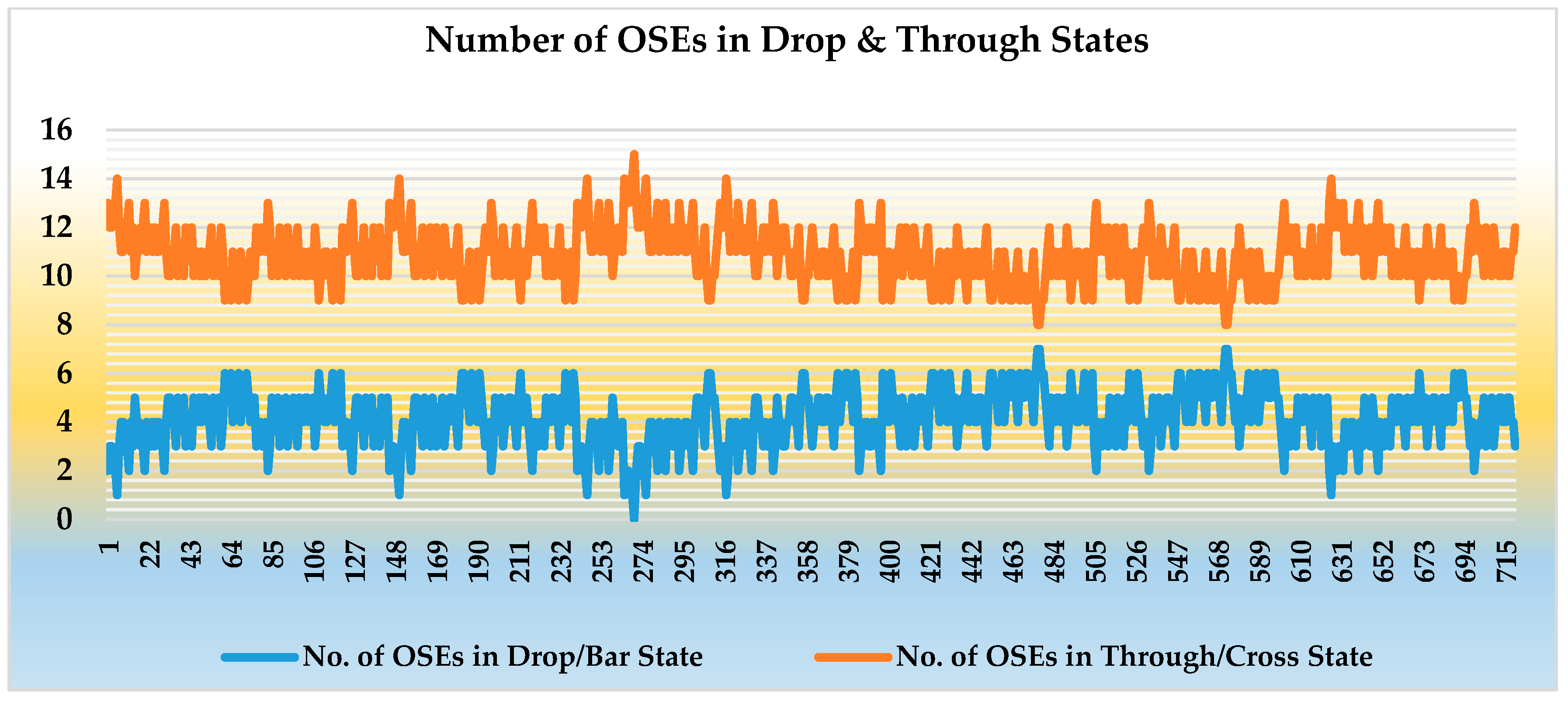
In optimal switching combinations, the numbers of OSEs in drop/bar and through/cross states for optimized HCROS are shown in Figure 10, where it can be observed that, similar to un-optimized HCROS, for the SC3 I/O link, all 12 OSEs are found in the through/cross state while no OSE is found in the drop/bar state. An important point in the case of optimized HCROS is that for some I/O permutations in optimized HCROS, maximum and optimal switching combinations are the same, i.e., 6 OSEs in drop/bar states and 6 in drop/through states, which means the maximum combination is the optimal switching combination in optimized HCROS. However, optimized HCROS still performs better than un-optimized HCROS in terms of power consumption and insertion loss due to reduced number of OSEs.

6. Comparisons, Analysis and Simulation Results

In this section, we compare the proposed HCROS with different non-blocking switch architectures, i.e., Spanke-Benes [30], cross switch matrix [31], PILOSS [32] and recently proposed 6-port optical switches/routers in [24,36]. In addition, we also analyzed the performance of the proposed HCROS in terms of IL and power consumption.

6.1. Calculation of Insertion Loss and Power Consumption for HCROS

In this article, we assumed that the IL and power consumption of 2 × 2 MR based OSE are as per the specifications listed in Table 8. The values shown are the result of experimental measurements and incorporate the effect of process variations caused by physical parameters [38].
In the rest of this article, our results and analysis rely on the specifications provided in Table 8.

6.2. Comparisons, Results and Analysis

We compared the proposed HCROS with cross switch matrix, Spanke-Benes, PILOSS and different optical switches/routers non-blocking switches with the same port count, i.e., N = 6. We calculated the total number of OSEs used in each architecture, estimated the number of waveguide crossings and maximum per path utilization of number of OSEs in each design. Numerical values of the above-mentioned parameters are listed in Table 9. We can observe in Table 9, that the proposed HCROS in its un-optimized form consumes less OSEs than the cross switch matrix [31] and PILOSS [32] which is almost 58% lower and the same compared to Spanke-Benes [30]. However, in optimized form there is a 66%, 50% and 20% reduction in OSEs in comparison to the cross switch matrix/PILOSS, six port router [24] and Spanke-Benes switch architectures, respectively. The number of per path OSEs was also reduced from 7 to 5 with a maximum of 3 OSEs in the drop/bar state for optimized HCROS, which helps to minimize the overall power consumption of switch architecture. The stage count of optimized HCROS in terms of OSEs is also minimized as compared to un-optimized HCROS, which alleviates the impact of IL in switch network.
We undertook a performance analysis of 6-port optical switches/routers in terms of power consumption, maximum insertion loss and minimum insertion loss. For evaluation of the performance parameters, the 2 × 2 micro-ring based OSE was taken as the basic element discussed in Section 2 of the manuscript. We chose the worst-case scenario, which determines the maximum power and loss overhead of 6 × 6 routers. We assumed all OSEs are in a drop/bar state, where maximum power is consumed in switch/router architecture and the maximum effect of insertion loss can be monitored. Maximum power consumption is calculated as the sum of all the OSEs in drop/bar state. Maximum insertion loss is calculated as the sum of all OSUs in drop/bar state while minimum loss is calculated as the sum of all OSEs in through/cross state. Effect of waveguide crossings is also included in the calculation of maximum and minimum insertion loss. The performance analysis of different 6-port routers is shown in Table 10. It can be observed from Table 10 that the optimized HCROS has better performance among the different 6-port optical switches/routers, with minimized power consumption and IL. HCROS has the advantage of routing all 6! = 720 I/O links as compared to the router architectures proposed in [24,36] which do not support that feature, therefore they are not included in the performance analysis shown in Table 10. We can observe a significant difference in performance parameters between HCROS and other switches/routers designs as shown in Table 10, therefore, detailed analysis for all 720 routing states is constrained to un-optimized and optimized HCROS.

6.3. Power Consumption of HCROS

We calculated the maximum and optimal power consumption for un-optimized and optimized HCROS designs. For the total power P consumption, we used the following Equation (10).
P = P D + P T
where PD is the power consumption of OSEs in a drop/bar state while PT is the power consumption of OSEs in through/cross state. Based on the switching combinations of un-optimized and optimized HCROS for different I/O links, we present the maximum and optimal power consumption in Table 11.
Based on the power calculations given in Table 11 and specification parameters assumed in Table 8, we calculated the maximum PMax_UO_HCROS/PMax_O_HCROS and optimal POpt_UO_HCROS/POpt_O_HCROS power consumptions in all 6 switching combinations for un-optimized and optimized HCROS architectures, respectively, and the results are shown in Figure 11. PMax_UO_HCROS, PMax_O_HCROS, POpt_UO_HCROS and POpt_O_HCROS are defined as follows.
  • PMax_UO_HCROS is the maximum power consumption in un-optimized HCROS
  • PMax_O_HCROS is the maximum power consumption in optimized HCROS
  • POpt_UO_HCROS is the optimal power consumption in un-optimized HCROS
  • POpt_O_HCROS is the optimal power consumption in optimized HCROS
Significant improvement in power consumption is noted in the case of POpt_UO_HCROS, PMax_O_HCROS and POpt_O_HCROS as compared to PMax_UO_HCROS. We observed PMax_UO_HCROS as 3.0 mW for SC1 I/O link, which is minimized up to 0.6 mW in the case of PMax_O_HCROS and POpt_O_HCROS which is 80% lower than PMax_UO_HCROS. Since some of the redundant switching states are lost as a result of optimization, therefore POpt_UO_HCROS and POpt_O_HCROS result in same power consumption for all I/O links, i.e., the number of OSEs used in drop/bar states are equal in both cases. Minimum power consumption is observed for I/O link SC3 in the case of POpt_UO_HCROS and POpt_O_HCROS, which means that for SC3 all OSEs are in a through/cross state and consume approximately negligible power, i.e., 0 mW in this case.
In addition to 6 I/O links, we calculated the power consumption of all 720 I/O links for un-optimized HCROS. Results are shown in Figure 12, where it can be observed that optimal reconfiguration of OSEs lead to minimum power consumption POpt_UO_HCROS in all 720 permutations. Maximum PMax_UO_HCROS of 3.0 mW of power consumption is observed for the 720th permutation, i.e., SC6. The optimal switching combination significantly reduces the power consumption of un-optimized HCROS.
Similarly, for optimized HCROS, the results of the optimal switching combination show a noteworthy improvement in power consumption POpt_O_HCROS as compared to PMax_O_HCROS. The results of all 720 I/O permutations are shown in Figure 13. It can be observed that in some cases, PMax_O_HCROS equals POpt_O_HCROS; this is because the fact maximum and optimal switching combinations of OSEs are equal, hence the same power is consumed in both cases. However, PMax_O_HCROS never crossed the POpt_O_HCROS, out of 720 I/O permutations 106 I/O permutations have the same power consumption, i.e., PMax_O_HCROS equals POpt_O_HCROS. In other words, we can conclude that 85% of the time, POpt_O_HCROS leads to minimum power consumption and 15% of the time, PMax_O_HCROS equals POpt_O_HCROS in optimized HCROS.
Finally, overall power savings for all 720 I/O links are shown in Figure 14. The difference between PMax_UO_HCROS and POpt_UO_HCROS is calculated and shown in blue, while the difference between PMax_O_HCROS and POpt_O_HCROS is presented in orange. A maximum power saving of 2.4 mW and 1.6 mW is reported in un-optimized and optimized HCROS, respectively, as a result of optimized reconfiguration.

6.4. Insertion Loss in HCROS

We estimated IL for un-optimized and optimized HCROS architectures as worst and optimal cases. First, we calculated total IL of the whole switch by considering OSEs in drop or through states for all 720 I/O links using the following Equation (11).
I L = I L C + I L D + I L T
Using algorithm-1, we can find more than one optimal switching combinations for one I/O link, so the appropriate combination can be selected and HCROS can be reconfigured according to the design requirements. Based on the results of Table 6, we chose one of the optimal switching combinations from each I/O links and this is shown in pictorial form for un-optimized HCROS architecture in Figure 15a–f, which is especially helpful in analyzing the effect of insertion loss of the proposed HCROS in both optimal un-optimized and optimized forms.
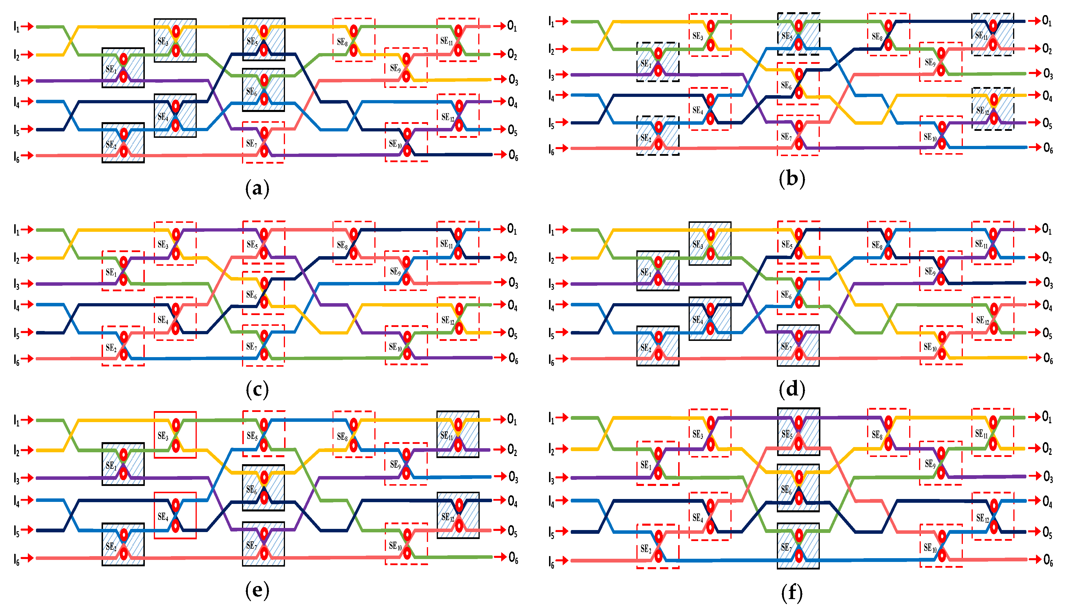
Similarly, one of the optimal routing combinations for each I/O link in the optimized HCROS architecture is shown in Figure 16a–f. We note that SC1/SC5 utilize a maximum of 6 OSEs in the drop/bar state and SC3 requires no OSE in the drop/bar state for optimal configuration, where all OSEs are in through/cross states that alleviate the effect of IL and minimize power consumption in optimized HCROS architecture.
IL is the sum of waveguide crossing loss (ILC) and loss induced due to switching states of OSE in drop (ILD) or through (ILT). Considering the switching states and waveguide crossings in switch architecture, ILS for each I/O link was estimated and listed in Table 12. We have defined certain terms for insertion loss calculation, i.e., ILMax_UO_HCROS, ILMax_O_HCROS, ILOpt_UO_HCROS, and ILOpt_O_HCROS are defined as follows:
  • ILMax_UO_HCROS is the maximum insertion loss in un-optimized HCROS
  • ILMax_O_HCROS is the maximum insertion loss in optimized HCROS
  • ILOpt_UO_HCROS is the optimal insertion loss in un-optimized HCROS
  • ILOpt_O_HCROS is the optimal insertion loss in optimized HCROS
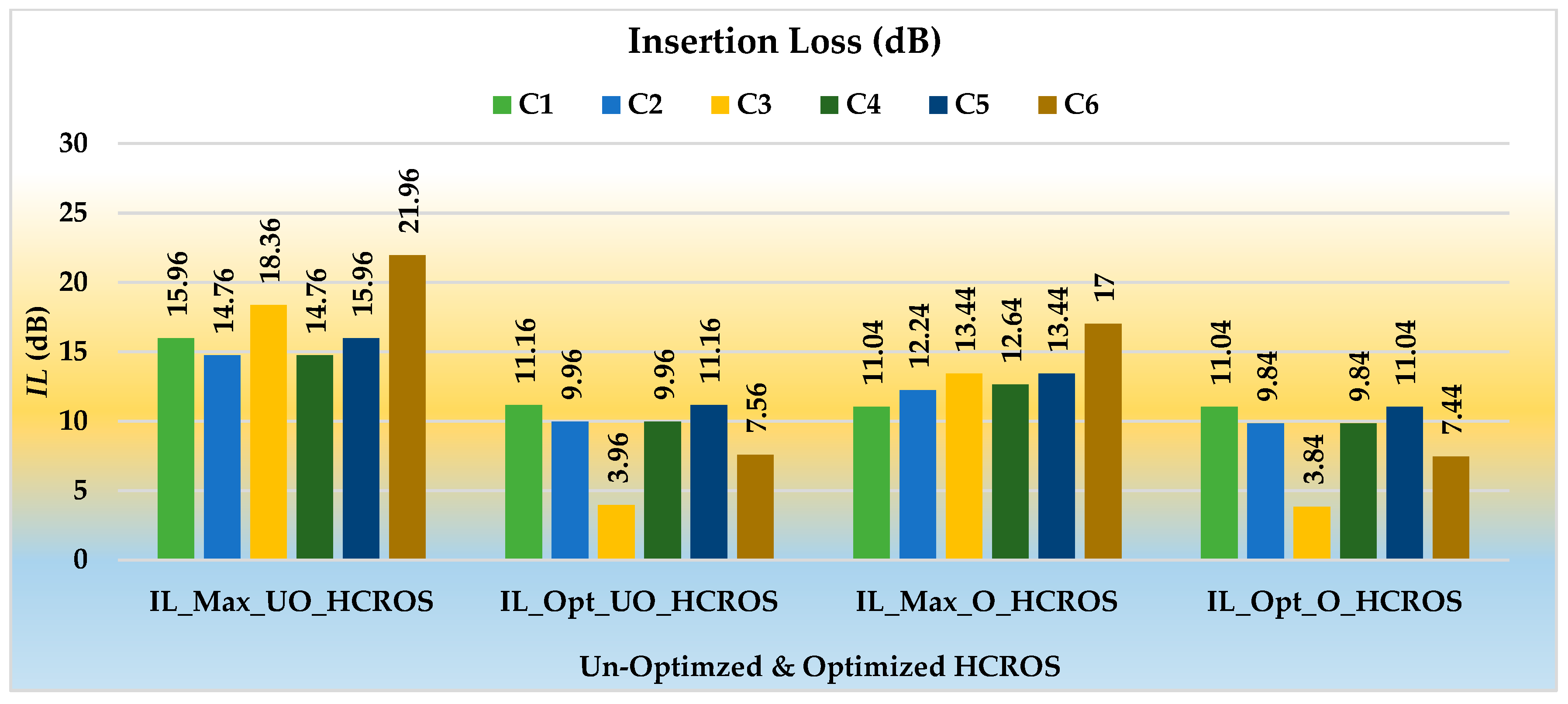
We counted the number of OSEs in drop/bar or through/cross and included 6 waveguide crossing losses in the case of un-optimized HCROS, and computed the maximum ILMax_UO_HCROS and optimal ILOpt_UO_HCROS losses in HCROS. Similarly, for optimized design, we determined the maximum and optimal losses denoted as ILMax_O_HCROS and ILOpt_O_HCROS. Expressions for each I/O link, showing the influence of insertion loss on switch architectures are listed in Table 12. Based on the calculations provided in Table 12, we analyzed the ILS induced in switch topologies. Detailed results are shown in Figure 17, where we observe that SC6 I/O link has a maximum IL of 21.96 dB in ILMax_UO_HCROS with 10 OSEs in drop states. ILOpt_UO_HCROS shows a significant improvement using fewer number of OSEs in drop states with a minimum value of 3.96 dB. ILMax_O_HCROS in comparison to ILMax_UO_HCROS shows major improvements and a maximum loss of 17 dB can be observed, which is 22.5% lower than ILMax_UO_HCROS for SC6 I/O link. Optimal optimized HCROS architecture loss ILOpt_O_HCROS shows the best performance of all, where the maximum value of 11.04 dB and minimum value of 3.84 dB are reported in the case of SC1/SC5 and SC3 I/O links, respectively, which is almost 37% and 79% lower than ILMax_UO_HCROS for the same configurations.
In addition to 6 I/O links, the analysis of insertion loss for all 720 I/O links for un-optimized HCROS is also presented. Results are shown in Figure 18, where can be seen that optimal reconfiguration of OSEs significantly minimizes insertion loss ILOpt_UO_HCROS in all 720 permutations. A maximum ILMax_UO_HCROS of 21.96 dB of insertion loss is observed for the 720th permutation, i.e., SC6. Notably, a reduction in insertion loss is observed for optimal switching combinations in un-optimized HCROS. Maximum insertion loss for optimal switching combinations ILOpt_UO_HCROS is observed as 12.36 dB while a minimum value of 3.96 dB was calculated.
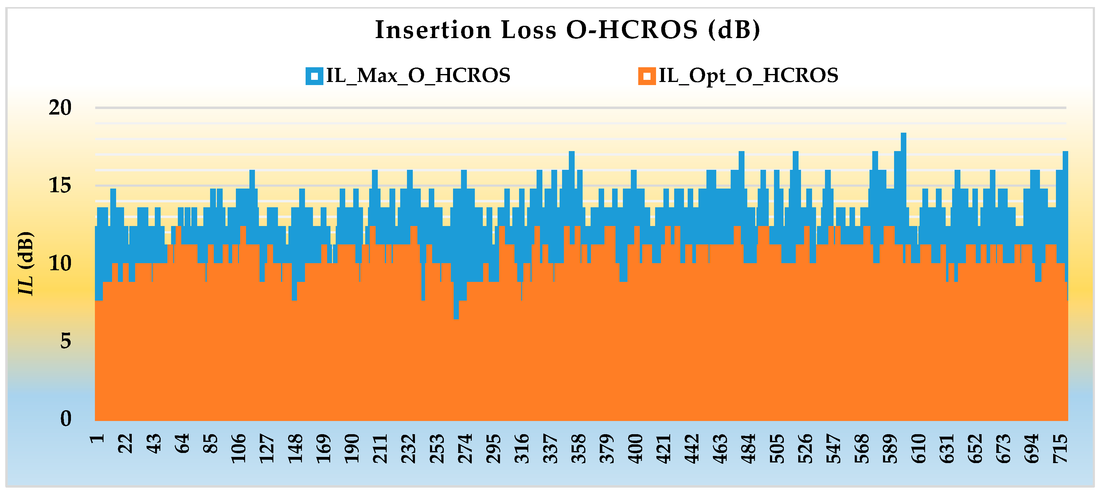
Similarly, the results of all 720 I/O permutations for optimized HCROS are shown in Figure 19. In some cases, similar to power consumption, ILMax_O_HCROS equals ILOpt_O_HCROS, since the maximum and optimal switching combinations of OSEs are equal, hence, the same insertion loss value is obtained in both cases. Out of a total 720 I/O permutations, 106 I/O permutations have the same insertion loss, i.e., ILMax_O_HCROS equals ILOpt_O_HCROS. In other words, 85% of the time ILOpt_O_HCROS remains better than ILMax_O_HCROS and 15% of the time ILMax_O_HCROS equals ILOpt_O_HCROS in optimized HCROS. However, ILMax_O_HCROS always remains lower than ILMax_UO_HCROS.
In addition, the average IL for every input to output path for 6 I/O links is presented. We calculated ILS for each input to output routing combination by counting the number of OSEs used in drop or through states and the number of waveguide crossing involved in particular I/O paths and finally, by taking the arithmetic mean of all input to output pairs for all specific I/O links using the following Equation (12).
I L A v g . = ( i = 1 , j = 1 n I L I i O j ) / n
For instance, we calculated average insertion loss, Avg. ILMax_UO_HCROS for SC1 I/O link, where IL for I1 → O2 is 5.8 dB, I2 → O3 is 7.52 dB, I3 → O4 is 2.28 dB, I4 → O5 is 6.64 dB, I5 → O6 is 7.52 dB and I6 → O1 is 2.16 dB and the average IL is 5.29 dB. In similar fashion, Avg. ILMax_O_HCROS for SC1 I/O link is observed as, I1 → O2 is 3.64 dB, I2 → O3 is 4.72 dB, I3 → O4 is 2.32 dB, I4 → O5 is 3.64 dB, I5 → O6 is 5.36 dB and I6 → O1 is 2.32 dB and the average IL is 3.67 dB. All the average losses for each input to output pair for all configurations are shown in Figure 20. Results presented in Figure 20 show that Avg.ILOpt_O_HCROS has a lower average IL for 6 I/O links. A minimum of 1.28 dB average loss for SC3 is reported which is almost 80% lower than Avg.ILMax_UO_HCROS.
The reduction in insertion loss for all 720 I/O links is shown in Figure 21. The difference between ILMax_UO_HCROS and ILOpt_UO_HCROS was calculated and is shown in blue, while the difference between ILMax_O_HCROS and ILOpt_O_HCROS is presented in orange in Figure 21. A maximum reduction of 14.4 dB and 9.6 dB insertion loss can be seen as a result of the optimized reconfiguration, in un-optimized and optimized HCROS, respectively.
A summary of maximum and minimum power consumption with power saving and maximum and minimum insertion loss with reduction for 720 I/O links in both un-optimized and optimized HCROS architectures is listed in Table 13. Our analysis shows that optimized HCROS with optimized reconfiguration with 12 OSEs shows significant improvements in overall power consumption and insertion loss in comparison to un-optimized HCROS. Up to 67% improvement in power consumption and 44% efficiency in insertion loss for optimized HCROS is reported. Similarly, a 33% power saving and reduction in insertion loss is also observed as in the optimized HCROS with optimal switching combinations.

7. Conclusions

In this article, we proposed an optimized reconfigurable architecture of a 6 × 6 optical switch called the HoneyComb optimized reconfigurable optical switch (HCROS) in different configurations. First, we presented an un-optimized architecture of HCROS using 15 OSEs and further optimized that design to reduce the number of OSEs to 12, which is an almost 20% reduction in overall OSEs. Furthermore, we proposed an algorithm to identify the minimum number of OSEs in an active drop/bar state to reconfigure the optical switch, which helps to alleviate the impact of insertion loss and provides power efficiency, and achieved an optimized reconfiguration. We compared the proposed HCROS with different non-blocking architectures, e.g., cross switch matrix, PILOSS, Spanke-Benes and different six-port switches/routers, where we found a maximum of 66% decrease in OSEs. Lastly, a comprehensive analysis of power consumption and insertion loss of HCROS in different configurations for 720 I/O links showed significant improvements in both parameters, i.e., power consumption and IL were reported in this article. This study could be utilized for a 6-port optical switch in the construction of cluster Mesh/3D ONoCs to meet the requirements of data transmission for future applications. In the future, we intend to extend this design in two ways (1) investigate the impact of HCROS on crosstalk noise and application mapping in ONoCs, and (2) explore the suitability of HCROS for Mach-Zehnder based OSEs.

Author Contributions

Conception, methodology and structure of this paper, M.R.Y.; Resources, N.W.; Supervision, N.W.; Writing—original draft, M.R.Y.; Validation, M.R.Y., G.Y., and T.A.; Software, M.R.Y., and T.A.; Investigation, M.R.Y., and G.Y.; Review and Editing, J.Z., T.A., and Y.Z.

Funding

This work was supported by the National Natural Science Foundation of China (No.61774086), the Natural Science Foundation of Jiangsu Province (BK20160806) and the Fundamental Research Funds for the Central Universities (NP2019102, NS2017023, NS2016041).

Acknowledgments

The authors would like to thank anonymous reviewers for their special effort. In addition, we would like to thank Inam-ul-Haq for his beneficial suggestions and comments.

Conflicts of Interest

The authors declare no conflict of interest.

References

  1. Arakawa, Y.; Nakamura, T.; Urino, Y.; Fujita, T. Silicon photonics for next generation system integration platform. IEEE Commun. Mag. 2013, 51, 72–77. [Google Scholar] [CrossRef]
  2. Nikolova, D.; Rumley, S.; Calhoun, D.; Li, Q.; Hendry, R.; Samadi, P.; Bergman, K. Scaling silicon photonic switch fabrics for data center interconnection networks. Opt. Express 2015, 23, 1159–1175. [Google Scholar] [CrossRef] [PubMed]
  3. Ro, Y.; Lee, E.; Ahn, J.H. Evaluating the Impact of Optical Interconnects on a Multi-Chip Machine-Learning Architecture. Electronics 2018, 7, 130. [Google Scholar] [CrossRef]
  4. Kayarkar, A.V.; Khurge, D.S. Router Architecture for the Interconnection Network: A Review. In Proceedings of the 2016 2nd International Conference on Computing, Communication, Control and Automation (ICCUBEA), Pune, India, 12–13 August 2016. [Google Scholar]
  5. Shacham, A.; Bergman, K.; Carloni, L.P. Photonic Networks-on-Chip for Future Generations of Chip Multiprocessors. IEEE Trans. Comput. 2008, 57, 1246–1260. [Google Scholar] [CrossRef] [Green Version]
  6. Fusella, E.; Cilardo, A. Lighting up On-Chip Communications with Photonics: Design Tradeoffs for Optical NoC Architectures. IEEE Circuits Syst. Mag. 2016, 16, 4–14. [Google Scholar] [CrossRef]
  7. Thraskias, C.A.; Lallas, E.N.; Neumann, N.; Schares, L.; Offrein, B.J.; Henker, R.; Plettemeier, D.; Ellinger, F.; Leuthold, J.; Tomkos, I. Survey of Photonic and Plasmonic Interconnect Technologies for Intra-Datacenter and High-Performance Computing Communications. IEEE Commun. Surv. Tutor. 2018, 20, 2758–2783. [Google Scholar] [CrossRef] [Green Version]
  8. Rumley, S.; Bahadori, M.; Polster, R.; Hammond, S.D.; Calhoun, D.M.; Wen, K.; Rodrigues, A.; Bergman, K. Optical interconnects for extreme scale computing systems. Parallel Comput. 2017, 64, 65–80. [Google Scholar] [CrossRef]
  9. Werner, S.; Navaridas, J.; Luján, M. A Survey on Optical Network-on-Chip Architectures. ACM Comput. Surv. 2017, 50, 1–37. [Google Scholar] [CrossRef]
  10. Yahya, M.R.; Wu, N.; Yan, G.; Yasir, Y. Review of Photonic and Hybrid on Chip Interconnects for MPSoCs in IoT Paradigm. In Proceedings of the 2018 21st Saudi Computer Society National Computer Conference (NCC), Riyadh, Saudi Arabiam, 25–26 April 2018; pp. 1–6. [Google Scholar]
  11. Zhou, T.; Jia, H.; Dai, J.; Yang, S.; Zhang, L.; Fu, X.; Yang, L. Rearrangeable-Nonblocking Five-Port Silicon Optical Switch for 2-D-Mesh Network on Chip. IEEE Photon. J. 2018, 10, 1–8. [Google Scholar] [CrossRef]
  12. Guo, P.; Hou, W.; Guo, L.; Yang, Q.; Ge, Y. Low Insertion Loss and Non-Blocking Microring-Based Optical Router for 3D Optical Network-on-Chip. IEEE Photon. J. 2018, 10, 1–10. [Google Scholar] [CrossRef]
  13. Jia, H.; Zhou, T.; Fu, X.; Ding, J.; Zhang, L.; Yang, L. Four-port mode-selective silicon optical router for on-chip optical interconnect. Opt. Express 2018, 26, 9740–9748. [Google Scholar] [CrossRef] [PubMed]
  14. Zhao, Y.; Jia, H.; Ding, J.; Zhang, L.; Fu, X.; Yang, L. Five-port silicon optical router based on Mach-Zehnder optical switches for photonic networks-on-chip. J. Semicond. 2016, 37, 114008. [Google Scholar] [CrossRef]
  15. Zhu, K.; Zhang, B.; Tan, W.; Gu, H. Votex: A non-blocking optical router design for 3D Optical Network on Chip. In Proceedings of the 2015 14th International Conference on Optical Communications and Networks (ICOCN), Nanjing, China, 3–5 July 2015; pp. 1–3. [Google Scholar]
  16. Jia, H.; Zhao, Y.; Zhang, L.; Chen, Q.; Ding, J.; Fu, X.; Yang, L. 5-port optical router based on Si microring optical switches for photonic networks-on-chip. IEEE Photon. Technol. Lett. 2016, 28, 947–950. [Google Scholar] [CrossRef]
  17. Dupuis, N.; Lee, B.G.; Rylyakov, A.V.; Kuchta, D.M.; Baks, C.W.; Orcutt, J.S.; Gill, D.M.; Green, W.M.J.; Schow, C.L. Modeling and Characterization of a Nonblocking 4×4 Mach–Zehnder Silicon Photonic Switch Fabric. J. Lightwave Technol. 2015, 33, 4329–4337. [Google Scholar] [CrossRef]
  18. Sathyadevaki, R.; Sundar, D.S.; Raja, A.S. Photonic crystal 4 × 4 dynamic hitless routers for integrated photonic NoCs. Photon. Netw. Commun. 2018, 36, 82–95. [Google Scholar] [CrossRef]
  19. Lipson, M.; Sherwood-Droz, N.; Poitras, C.B.; Biberman, A.; Lee, B.G.; Bergman, K. High-Speed 2 × 2 Switch for Multiwavelength Silicon-Photonic Networks-On-Chip. J. Lightwave Technol. 2009, 27, 2900–2907. [Google Scholar] [CrossRef]
  20. Jinguji, K.; Takato, N.; Sugita, A.; Kawachi, M. MachZehnder interferometer type opticalwaveguide coupler with wavelength-flattened coupling ratio. Electron. Lett. 1990, 26, 1326–1327. [Google Scholar] [CrossRef]
  21. Liang, L.; Zhang, K.; Zheng, C.T.; Zhang, X.; Qin, L.; Ning, Y.Q.; Zhang, D.M.; Wang, L.J. N × N Reconfigurable Nonblocking Polymer/Silica Hybrid Planar Optical Switch Matrix Based on Total-Internal-Reflection Effect. IEEE Photon. J. 2017, 9, 1–11. [Google Scholar] [CrossRef]
  22. Geng, M.; Tang, Z.; Chang, K.; Huang, X.; Zheng, J. N-port strictly non-blocking optical router based on Mach-Zehnder optical switch for photonic networks-on-chip. Opt. Commun. 2017, 383, 472–477. [Google Scholar] [CrossRef]
  23. Chen, Q.; Zhang, F.; Ji, R.; Zhang, L.; Yang, L. Universal method for constructing N-port non-blocking optical router based on 2 × 2 optical switch for photonic networks-on-chip. Opt. Express 2014, 22, 12614–12627. [Google Scholar] [CrossRef]
  24. Min, R.; Ji, R.; Yang, L.; Zhang, L.; Tian, Y.; Ding, J.; Chen, H.; Lu, Y.; Zhou, P.; Zhu, W. A universal method for constructing N-port non-blocking optical router based on microring resonators. J. Lightwave Technol. 2012, 30, 3736–3741. [Google Scholar] [CrossRef]
  25. Zhou, T.; Jia, H. Method to optimize optical switch topology for photonic network-on-chip. Opt. Commun. 2018, 413, 230–235. [Google Scholar] [CrossRef]
  26. Lin, B.C.; Chen, S.; Huang, Y.; Lea, C.T. Power Minimization in Microring-Based Benes Networks. IEEE Trans. Commun. 2018, 66, 3517–3525. [Google Scholar] [CrossRef]
  27. Lee, B.G.; Dupuis, N. Silicon Photonic Switch Fabrics: Technology and Architecture. J. Lightwave Technol. 2019, 37, 6–20. [Google Scholar] [CrossRef]
  28. Pattavina, A. Switching Theory—Architectures and Performance in Broadband ATM Networks; John Wiley & Sons Ltd.: Hoboken, NJ, USA, 1998; ISBN 0471963380. [Google Scholar]
  29. Benes, V. Algebraic and Topological Properties of Connecting Networks. Bell Syst. Tech. J. 1962, 41, 1249–1274. [Google Scholar] [CrossRef]
  30. Spanke, R.A.; Beneš, V.E. N-stage planar optical permutation network. Appl. Opt. 1987, 26, 1226–1229. [Google Scholar] [CrossRef]
  31. DasMahapatra, P.; Stabile, R.; Rohit, A.; Williams, K.A. Optical Crosspoint Matrix Using Broadband Resonant Switches. IEEE J. Sel. Top. Quantum Electron. 2014, 20, 1–10. [Google Scholar] [CrossRef]
  32. Shimoe, T. Path-independent insertion loss optical space switch. In Proceedings of the Optical Fiber Communication Conference, Reno, NV, USA, 19 January 1987. paper WB2. [Google Scholar]
  33. Ortín-Obón, M.; Suárez-Gracia, D.; Villarroya-Gaudó, M.; Izu, C.; Viñals-Yúfera, V. Analysis of network-on-chip topologies for cost-efficient chip multiprocessors. Microprocess. Microsyst. 2016, 42, 24–36. [Google Scholar] [CrossRef] [Green Version]
  34. Chittamuru, S.V.R.; Dang, D.; Pasricha, S.; Mahapatra, R.N. BiGNoC: Accelerating Big Data Computing with Application-Specific Photonic Network-on-Chip Architectures. IEEE Trans. Parallel Distrib. Syst. 2018, 29, 2402–2415. [Google Scholar] [CrossRef]
  35. Huang, L.; Wang, K.; Qi, S.; Gu, H.; Yang, Y. Panzer: A 6 × 6 photonic router for optical network on chip. IEICE Electron. Express 2016, 13, 20160719. [Google Scholar] [CrossRef]
  36. Yaghoubi, E.; Reshadi, M.; Hosseinzadeh, M. Mach–Zehnder-based optical router design for photonic networks on chip. Opt. Eng. 2015, 54, 035102. [Google Scholar] [CrossRef]
  37. Yahya, M.R.; Wu, N.; Yan, G.; Ge, F.; Ahmed, T. RoR: A low insertion loss design of rearrangeable hybrid photonic-plasmonic 6 × 6 non-blocking router for ONoCs. IEICE Electron. Express 2019, 16, 1–5. [Google Scholar] [CrossRef]
  38. Yuen, P.-H.; Chen, L.-K. Optimization of Microring-Based Interconnection by Leveraging the Asymmetric Behaviors of Switching Elements. J. Lightwave Technol. 2013, 31, 1585–1592. [Google Scholar] [CrossRef]
  39. Yang, Y.; Chen, K.; Gu, H.; Zhang, B.; Zhu, L. TAONoC: A Regular Passive Optical Network-on-Chip Architecture Based on Comb Switches. IEEE Trans. Very Large Scale Integr. Syst. 2018, 27, 954–963. [Google Scholar] [CrossRef]
  40. Zhang, L.; Tan, X.; Yang, M.; Qi, M.; Hu, T.; Yang, J. On-Chip Wavelength-Routed Photonic Networks with Comb Switches. In Proceedings of the 9th International Conference on Group IV Photonics (GFP), San Diego, CA, USA, 29–31 August 2012; Volume 14, pp. 279–281. [Google Scholar]
  41. Jia, H.; Zhou, T.; Zhao, Y.; Xia, Y.; Dai, J.; Zhang, L.; Ding, J.; Fu, X.; Yang, L. Six-port optical switch for cluster-mesh photonic network-on-chip. Nanophotonics 2018, 7, 827–835. [Google Scholar] [CrossRef]
  42. Jajszczyk, A. Rearrangeable Clos Networks: Fifty Years of the Theory Evolution. IEEE Commun. Mag. 2003, 41, 28–33. [Google Scholar] [CrossRef]
  43. Lin, B.C. Rearrangeable W-S-W Elastic Optical Networks Generated by Graph Approaches. J. Opt. Commun. Netw. 2018, 10, 675–685. [Google Scholar] [CrossRef]
  44. Bogaerts, W.; Van Thourhout, D.; Dumon, P.; Baets, R. Low-loss, low-cross-talk crossings for silicon-on-insulator nanophotonic waveguides. Opt. Lett. 2007, 32, 2801–2803. [Google Scholar] [CrossRef] [Green Version]
Figure 1. 2 × 2 OSE. (a) MR OSE drop/bar state. (b) MR OSE through/cross state.
Electronics 08 00844 g001
Figure 2. 6 × 6 HCROS Optical switch architecture with 15 OSEs.
Electronics 08 00844 g002
Figure 3. 6 × 6 Optical switch architecture with all 15 OSEs in drop/bar state.
Electronics 08 00844 g003
Figure 4. 6 × 6 Optimized optical switch architecture with 12 OSEs.
Electronics 08 00844 g004
Figure 5. Routing example of I/O link SC6 for straight mapping.
Electronics 08 00844 g005
Figure 6. N × N switch divided into two layers of (N-2) × (N-2) and 2 × 2.
Electronics 08 00844 g006
Figure 7. Number of total and optimal switching combinations in un-optimized HCROS.
Electronics 08 00844 g007
Figure 8. Number of OSEs in drop/bar and through/cross states in optimal switching combinations for un-optimized HCROS.
Electronics 08 00844 g008
Figure 9. Number of total and optimal switching combinations in optimized HCROS.
Electronics 08 00844 g009
Figure 10. Number of OSEs in drop/bar and through/cross states in optimal switching combinations for optimized HCROS.
Electronics 08 00844 g010
Figure 11. Power consumption P (mW) of un-optimized and optimized HCROS for 6 I/O links.
Electronics 08 00844 g011
Figure 12. Power consumption PMax_UO_HCROS and POpt_UO_HCROS for all 720 I/O links in un-optimized HCROS.
Electronics 08 00844 g012
Figure 13. Power consumption PMax_O_HCROS and POpt_O_HCROS for all 720 I/O links in optimized HCROS.
Electronics 08 00844 g013
Figure 14. Power savings in un-optimized and optimized HCROS for all 720 I/O links.
Electronics 08 00844 g014
Figure 15. Optimal switching combinations of I/O links in un-optimized HCROS. (a) I/O link SC1 with 6 OSEs in drop/bar state. (b) I/O link SC2 with 5 OSEs in drop/bar state. (c) I/O link SC3 with all OSEs in through/cross state. (d) I/O link SC4 with 5 OSEs in drop/bar state. (e) I/O link SC5 with 6 OSEs in drop/bar state. (f) I/O link SC6 with 3 OSEs in drop/bar state. (Note: all OSEs in drop/bar state are shown in solid line with gradient fill).
Electronics 08 00844 g015
Figure 16. Optimal switching combinations of I/O links in optimized HCROS. (a) I/O link SC1 with 6 OSEs in drop/bar state. (b) I/O link SC2 with 5 OSEs in drop/bar state. (c) I/O link SC3 with all OSEs in through/cross state. (d) I/O link SC4 with 5 OSEs in drop/bar state. (e) I/O link SC5 with 6 OSEs in drop/bar state. (f) I/O link SC6 with 3 OSEs in drop/bar state.
Electronics 08 00844 g016
Figure 17. Maximum insertion loss IL (dB) of un-optimized and optimized HCROS for 6 I/O links.
Electronics 08 00844 g017
Figure 18. Insertion loss ILMax_UO_HCROS and ILOpt_UO_HCROS for all 720 I/O links in un-optimized HCROS.
Electronics 08 00844 g018
Figure 19. Insertion Loss ILMax_O_HCROS and ILOpt_O_HCROS for all 720 I/O links in optimized HCROS.
Electronics 08 00844 g019
Figure 20. Average insertion loss IL(dB) of un-optimized and optimized HCROS for all I/O links.
Electronics 08 00844 g020
Figure 21. Insertion loss reduction in un-optimized and optimized HCROS for all 720 I/O links.
Electronics 08 00844 g021
Table 1. MR based 2 × 2 OSE switching state table.
InputOutputMR StateWavelength λi
I1O1DB *λi = λr
I2O2DB *λi = λr
I1O2TC *λi ≠ λr
I2O1TC *λi ≠ λr
* Drop/Bar (DB) and Through/Cross (TC) states.
Table 2. Routing combinations for the 6-port optical switch.
I/O LinksRouting Combinations
SC1I1 → O2; I2 → O3; I3 → O4; I4 → O5; I5 → O6; I6 → O1;
SC2I1 → O3; I2 → O4; I3 → O5; I4 → O6; I5 → O1; I6 → O2;
SC3I1 → O4; I2 → O5; I3 → O6; I4 → O1; I5 → O2; I6 → O3;
SC4I1 → O5; I2 → O6; I3 → O1; I4 → O2; I5 → O3; I6 → O4;
SC5I1 → O6; I2 → O1; I3 → O2; I4 → O3; I5 → O4; I6 → O5;
SC6I1 → O1; I2 → O2; I3 → O3; I4 → O4; I5 → O5; I6 → O6;
Table 3. Switching combinations of OSEs for a particular I/O link in the 6-port HCROS.
I/O LinksSE1SE2SE3SE4SE5SE6SE7SE8SE9SE10SE11SE12SE13SE14SE15
SC1DBDBDBDBDBDBDBDBTCDBDBTCTCTCTC
SC2DBDBDBDBDBDBDBTCTCTCTCTCTCDBDB
SC3DBDBDBDBDBDBTCTCTCDBDBDBDBDBDB
SC4DBDBDBDBDBDBTCTCDBDBDBTCTCTCTC
SC5DBDBDBDBDBDBTCDBDBTCTCTCTCDBDB
SC6DBDBDBDBDBDBDBDBDBDBDBDBDBDBDB
Table 4. Switching combinations of OSEs for particular I/O links in the 6-port optimized HCROS.
I/O LinksSE1SE2SE3SE4SE5SE6SE7SE8SE9SE10SE11SE12
SC1DBDBDBDBDBDBTCTCTCTCTCTC
SC2TCTCDBDBTCTCDBDBDBDBDBTC
SC3DBDBDBDBTCTCTCDBDBDBTCDB
SC4DBDBDBDBTCTCDBTCTCTCTCTC
SC5TCTCDBDBDBDBTCDBDBDBDBTC
SC6DBDBDBDBDBDBDBDBDBDBTCDB
Table 5. Algorithm-1 to identify the optimal switching combination.
Inputs:N, s, ek, Ci
Outputs:Nc, Nd, Dc
Procedure:
1. Determine Ns = k = 1 K e k
2. Find St = 2Ns
3. Define ETs and EDs using Equation (3)
4. Compute Md for Ci using Equation (4) and Table 2
5. Set Nc = 0 to find total number of combinations
6. Loop i = 1 to St
7.   Choose Ci.
8.   Loop j = 1 to Ns
9.     if (Ci(j) = 0)
10.      SE(j) = ETs using Equation (1)
11.     else
12.      SE(j) = EDs using Equation (2)
13.   end
14.   Get Ω1, Ω2, … ΩS using SE(j) for every switching stage using Equation (5).
15.   Calculate M = Ω1, Ω2, … ΩS using Equation (4)
16.     If (M = Md)
17.      Nc = Nc + 1
18.      Store Ci
19.     else
20.      Ignore Ci.
21.   Determine Nd.
22.   Find Dc = Ci (min(ED)).
23. end
Table 6. Analysis of optimal switching combinations in un-optimized HCROS.
I/O LinksTotal Possible CombinationsNo. of Optimal CombinationsNo. of OSEs in Drop/Bar StateNo. of OSEs in Through/Cross State
SC1341469
SC23414510
SC31441015
SC43414510
SC5341469
SC61441312
Table 7. Analysis of optimal switching combinations in optimized HCROS.
I/O LinksTotal CombinationsNo. of Optimal CombinationsNo. of OSEs in Drop/Bar StateNo. of OSEs in Through/Cross State
SC13366
SC29757
SC3181012
SC43357
SC59766
SC618139
Table 8. Specifications and performance parameters.
ParametersDrop/Bar StateThrough/Cross State
Power Consumption of OSEPDPT
200 µW [38]0 W [38]
Insertion Loss of OSEILDILT
1.4 dB [38]0.2 dB [38]
IL of Waveguide CrossingILC
0.16 dB [44]
Table 9. Hardware cost comparisons and analysis for N = 6.
Switch TopologyTotal OSEsWaveguide CrossingsMax. OSEs in one Path
PILOSS [32]36306
Cross Switch Matrix [31]36011
Reference [24]24244
Spanke-Benes [30]1506
Reference [36]12114
RoR [37]1587
HCROS Un-Optimized1567
HCROS Optimized1295
Table 10. Performance analysis of 6-port optical switches/routers.
Switch TopologyMaximum Power (mW)Maximum Insertion Loss (dB)Minimum Insertion Loss (dB)
PILOSS [32]7.255.212
Cross Switch Matrix [31]7.250.47.2
Spanke-Benes [30]3.0213.0
RoR [37]3.022.284.28
HCROS Un-Optimized3.021.963.96
HCROS Optimized2.418.243.84
Table 11. Power consumption of OSEs in HCROS.
I/O LinksHCROS Un-OptimizedHCROS Optimized
Maximum
(PMax_UO_HCROS)
Optimal
(POpt_UO_HCROS)
Maximum
(PMax_O_HCROS)
Optimal
(POpt_O_HCROS)
SC110*PD + 5*PT6*PD + 9*PT6*PD + 6*PT6*PD + 6*PT
SC29*PD + 6*PT5*PD + 10*PT7*PD + 5*PT5*PD + 7*PT
SC312*PD + 3*PT15*PT8*PD + 4*PT12*PT
SC49*PD + 6*PT5*PD + 10*PT5*PD + 7*PT5*PD + 7*PT
SC510*PD + 5*PT6*PD + 9*PT8*PD + 4*PT6*PD + 6*PT
SC615*PD3*PD + 12*PT11*PD + 1*PT3*PD + 9*PT
Table 12. Insertion loss of OSEs in HCROS.
I/O LinksHCROS Un-OptimizedHCROS Optimized
Maximum
(ILMax_UO_HCROS)
Optimal
(ILOpt_UO_HCROS)
Maximum
(ILMax_O_HCROS)
Optimal
(ILOpt_O_HCROS)
SC16*ILC + 10*ILD + 5*ILT6*ILC + 6*ILD + 9*ILT9*ILC + 6*ILD + 6*ILT9*ILC + 6*ILD + 6*ILT
SC26*ILC + 9*ILD + 6*ILT6*ILC + 5*ILD + 10*ILT9*ILC + 7*ILD + 5*ILT9*ILC + 5*ILD + 7*ILT
SC36*ILC + 12*ILD + 3*ILT6*ILC + 15*ILT9*ILC + 8*ILD + 4*ILT9*ILC + 12*ILT
SC46*ILC + 9*ILD + 6*ILT6*ILC + 5*ILD + 10*ILT9*ILC + 5*ILD + 7*ILT9*ILC + 5*ILD + 7*ILT
SC56*ILC + 10*ILD + 5*ILT6*ILC + 6*ILD + 9*ILT9*ILC + 8*ILD + 4*ILT9*ILC + 6*ILD + 6*ILT
SC66*ILC + 15*ILD6*ILC + 3*ILD + 12*ILT9*ILC + 11*ILD + 1*ILT9*ILC + 3*ILD + 9*ILT
Table 13. Maximum/minimum power consumption with power saving and maximum/minimum insertion loss with reduction for 720 I/O links.
ParameterHCROS Un-OptimizedHCROS Optimized
Power (mW)Maximum/MinimumMaximum
(PMax_UO_HCROS)
Optimal
(POpt_UO_HCROS)
Maximum
(PMax_O_HCROS)
Optimal
(POpt_O_HCROS)
Max. Power3.01.42.41.4
Min. Power1.200.60
Insertion Loss (dB)Maximum/MinimumMaximum
(ILMax_UO_HCROS)
Optimal
(ILOpt_UO_HCROS)
Maximum
(ILMax_O_HCROS)
Optimal
(ILOpt_O_HCROS)
Max. IL21.9612.3618.2412.24
Min. IL11.163.967.443.84
Power Saving (mW)Maximum/MinimumDifference
(PDiff_MaxtoOpt_UO_HCROS)
Difference
(PDiff_MaxtoOpt_O_HCROS)
Max. Power Saving2.41.6
Min. Power Saving0.40
Insertion Loss Reduction (dB)Maximum/MinimumDifference
(ILDiff_MaxtoOpt_UO_HCROS)
Difference
(ILDiff_MaxtoOpt_O_HCROS)
Max. IL Reduction14.49.6
Min. IL Reduction2.40