Behavior of ISOP, IPOS and ISOS configurations with respect to CSC dispersion is going to be reported in this section. As introduced, the set of 3 × 3 CSCs characterized above is considered for that. Several CSC configurations are going to be implemented in a specific test bench before to be compared. First of all, IPOS configuration will be tested with many CSCs arrangements in both open and closed loop operations. Then most relevant configurations will be also tested in ISOP and ISOS configuration to see if there is any additional information to gather. Testing is based on a second specific motherboard, fully instrumented, to be able to sense all voltages and all currents on each CSC. A specific design of experiment is developed to cover a wide range of configurations but not all of them. The observed parameters are the PCA voltage and current distribution over the CSCs and the converter total losses. These observed parameters will be compared to that of the respective CSCs implemented in each experiment.
4.1. Design of Experiment
The design of experiment has to answer the following criteria. It must be representative of a large set of possible CSC arrangement while remaining concise in volume. In this part, one must understand “arrangement” but the relative positions that each of the CSC families are occupying in the association. The number of CSCs implemented in each test must remain reasonable but representative enough.
Three families of 3 CSCs have been selected from the 3 extremes quintiles (explained in
Section 3.2) in the Gaussian distribution and have been further characterized. Each CSC is named CSC
y,z, where the y variable represents the family letter (A, B and C) and the z variable represents the number of the CSC in that family (1, 2 and 3). With 9 CSCs, arrangements above 360k are still possible. This is not possible and the experiment must be narrowed.
Table 5 below describes the design of experiment that has been defined. For each test, 3 sub tests are carried out using 3 sets of CSCs in order to confirm observations. Basically, each CSC family is implemented to highlight the impact of paired CSCs over the distribution range. Only open loop control is investigated in this paper. Then, family mixes are tested. At first, one extreme quintile CSC is introduced in the association. Then one CSC of each family is tested. Finally, respective position of CSCs are changed in order to investigate if the CSC position has an impact.
Table 5 does not includes all measurements obtained in order to save some space in the article but also to concentrate data and ease comparisons.
4.2. Bench and Mother Board for Plug and Play ISOP/IPOS/ISOS Configuration Testing
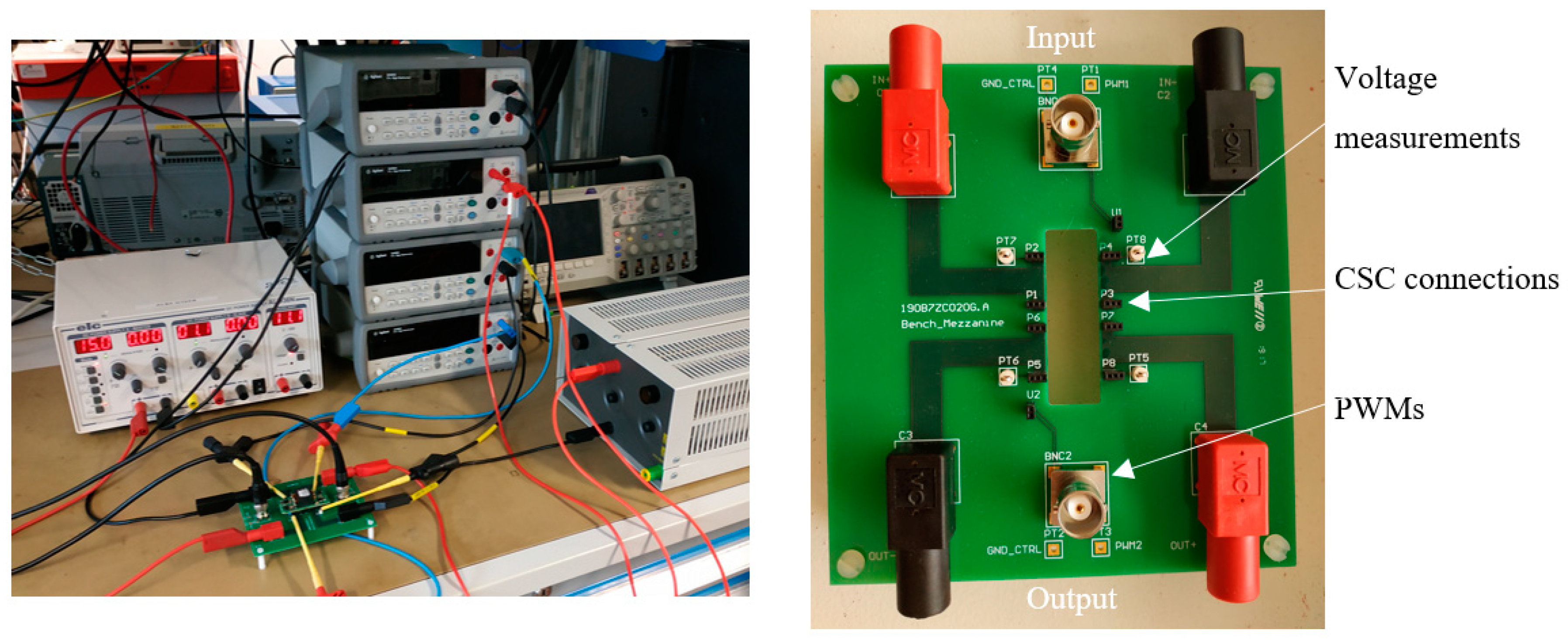
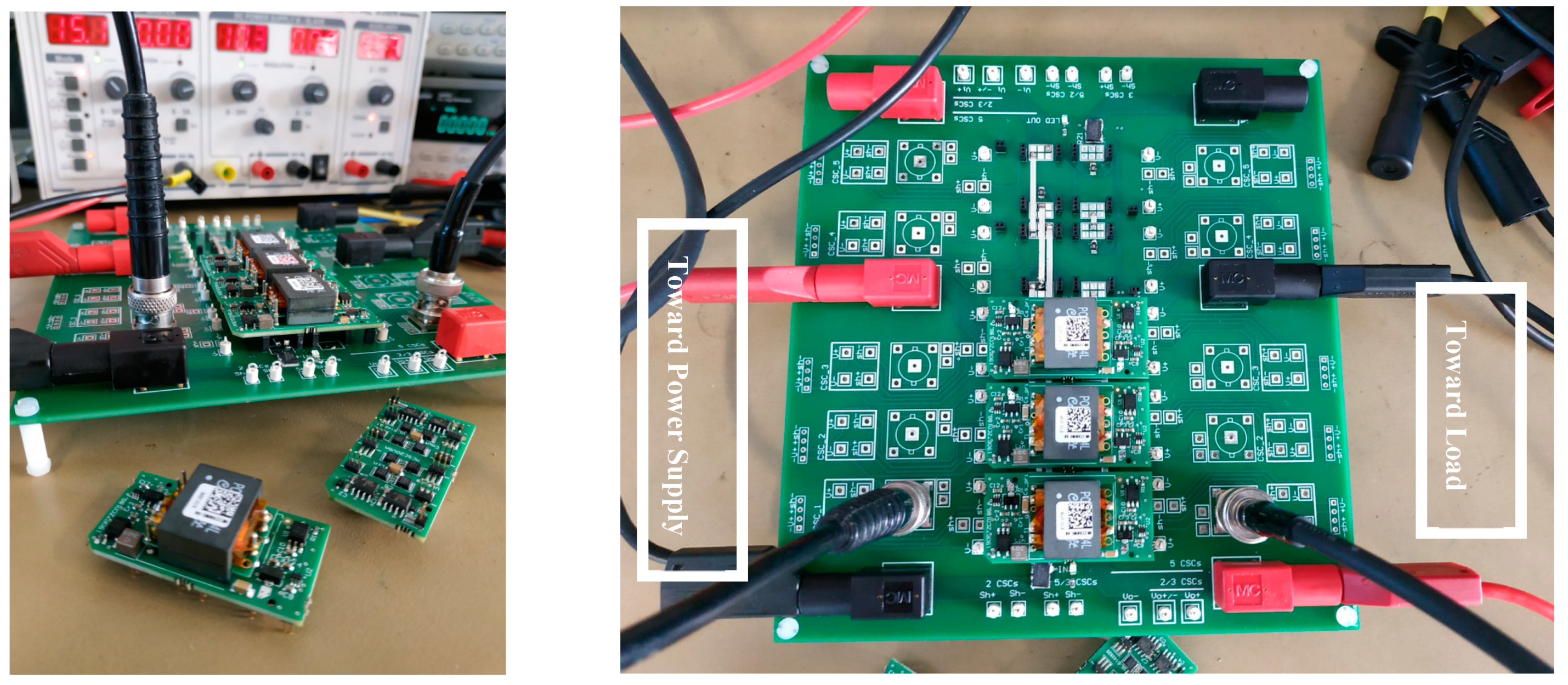
In order to associate and interconnect from the electric point of view the cells presented above to see the impact of the disparity of the components, a test bench has been designed. The test bench used in this test was designed for the balancing test campaign for from 2 up to 5 cells. A mother board was designed to enable any configuration and to ease arrangements. It is presented in
Figure 8. This one can implement different configurations (ISOP, IPOS, ISOS) by soldering components not presented in this article. The characteristics are as follows:
From 2 up to 5 CSCs can be implemented and fully instrumented;
Any configuration (IPOS, ISOP, ISOS);
Each cell is instrumented with the same input and output voltage and current measurements device (shunt and kelvin measurements);
Always the same measurement device are used for the whole experiment and it is always used to measure the same parameters;
Possibility to apply the same driver signals to the arrangement or possibility to differentiate all of them.
Extreme care was applied to minimize the impact of the mother board. Especially the electrical interconnection among the CSC are carried out with large current rating jumpers, offering very low equivalent resistance (less than 1 mΩ per jumper). Since CSCs are associated on their DC sides, the parasitic inductance of these jumpers has not been considered and further characterized. Indeed, only open loop and steady state operations are considered in this work, where current flowing through jumpers is almost purely DC. As a consequence it is assumed that the inductive contribution of interconnects among CSCs can be neglected. Also, the CSCs are not soldered on the mother board in order to enable and ease the implementation of many arrangement with the same families. For that a specific socket pattern was developed in order to receive the CSC. The impact of such a electrical contact has been carefully checked. The equivalent series resistance of the socket was measured several time over the experiments and remained close to 2 mΩ. The relatively stable value of the resistance, applied in series with all CSC implemented on the board, offers a limited impact. Without being totally negligible, it was not possible to improve further our test bench without a significant complexity in terms of implementation.
All voltage and current (kelvin point on shunt) measurements are carried out with the same 5 digits multi-meters in order to make relative comparison possible. For example, multi-meter 1 always measures CSC input voltage, and so on and so forth. Only up to 3 or 5 CSCs are tested on this bench in order to keep identical the measurements devices and to avoid difficult calibration among measurements devices. This approach, combined with care and methodology, ensures reproducible as well as comparable measurement.
The tests followed the experimental design defined in
Table 5. This test was realized in two operating points that are closed to Test 1 and Test 3. Only the main result are shown in this section.
4.3. Experimental Results
Many different studies and analysis can be carried out with the CSC batch that has been produced and characterized. In the following section we are reporting on the very first observations that have been done in a tentative way to illustrate in the most accessible approach.
4.3.1. Electrical Balance Operating Point
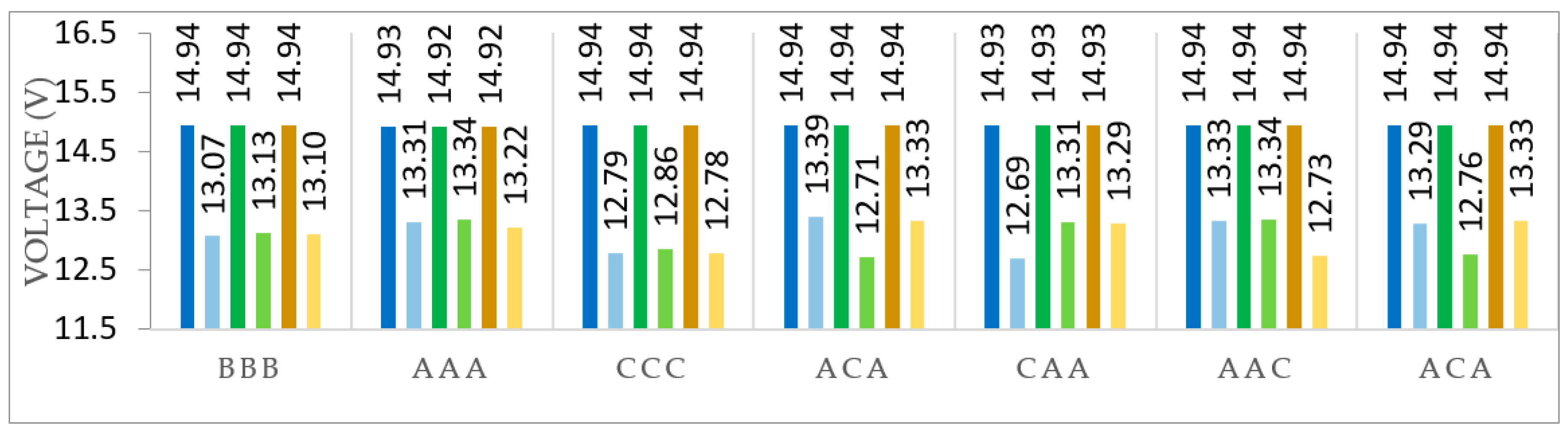
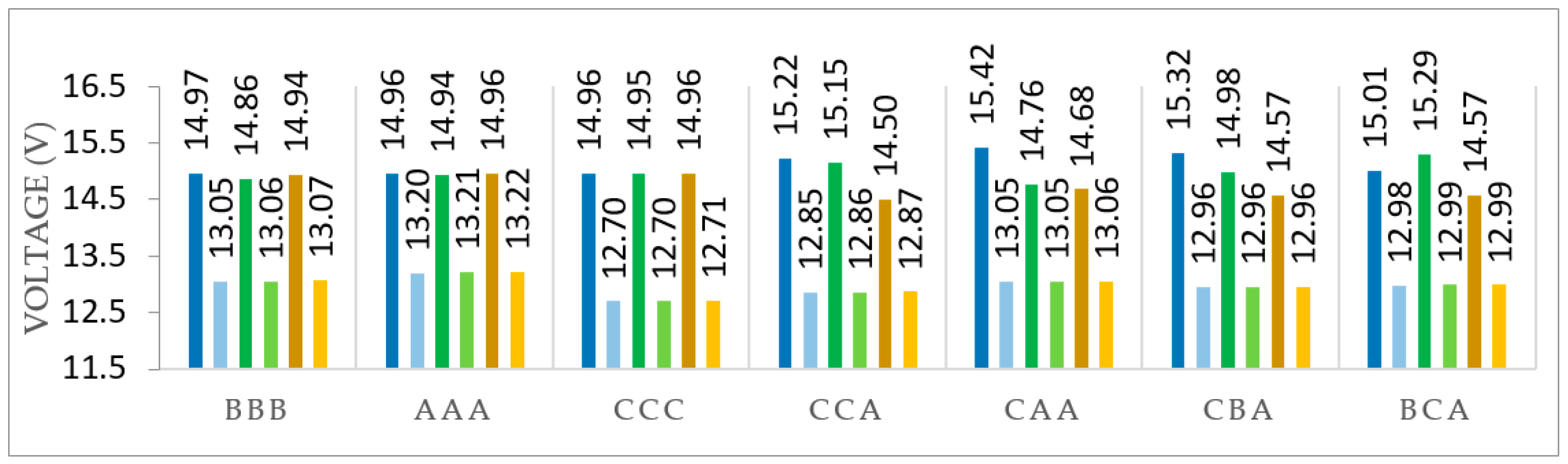
In
Figure 9 below, a first set of arrangement testing in IPOS configuration is provided. Several arrangements of 3 CSCs from various families are tested. The letter at the bottom of each test describes the arrangement with respect to the family name. Since it does not add a significant complement, the number of the CSC within the family is not depicted here to optimize the amount of data made available. Each CSC in the arrangement has a color code: blue colors corresponds to the first CSC in the network, green, the second one and yellow the third one. Dark colors counts for input voltage whereas light colors stands for output voltage level. 7 arrangements are displayed. For example, in arrangement number 4, CSC number 2 is coming from family C and has an input voltage of 14.94 V and an output voltage of 12.71V.
In the IPOS configuration, input voltage is fixed by the supply and is equal for all CSCs implemented. In this configuration, for all arrangement, there is a quite good correspondence between the behavior of the CSC when it is implemented alone and when it is implemented into a network. No matter the arrangement and the family, there is almost no issue observed in this configuration. Only a little increase in tendencies can be observed.
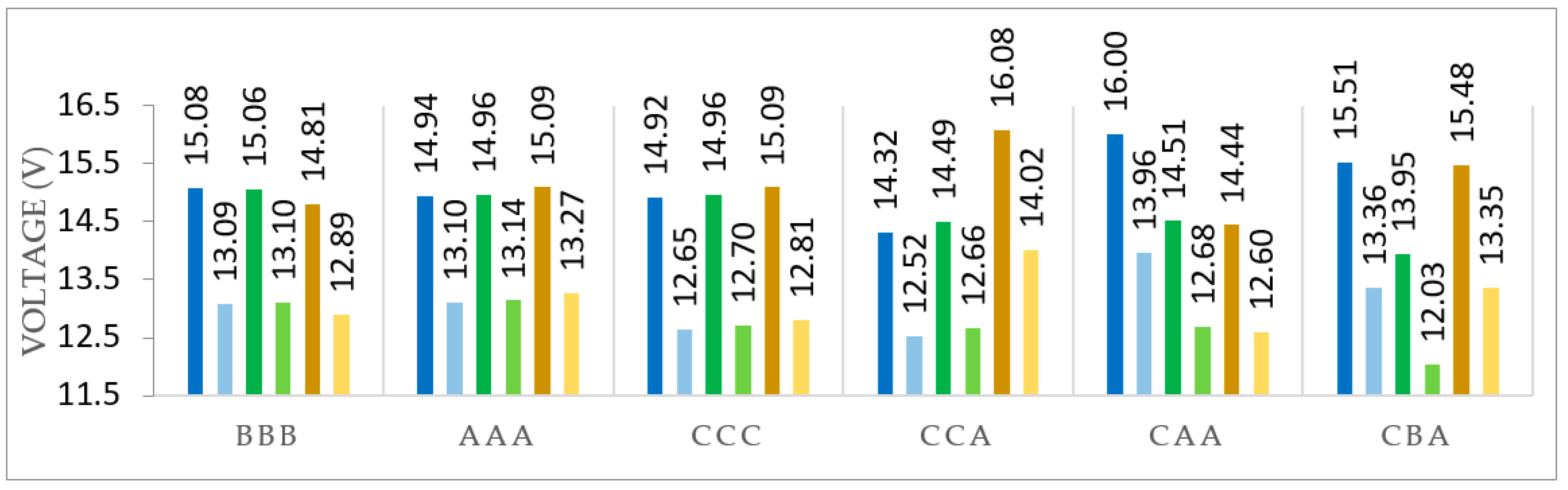
When the ISOP configuration is implemented, the input voltage is no more fixed. It is now the output voltage that is made common to all CSCs due to the selected configuration. In an open loop, R load primary to secondary phase shift are fixed, together with the total input voltage, equal to 45 V. In that case, the output voltage is left free to stabilize at any voltage level, as well as the CSC input voltages that only constraint is that the sum must remain equal to 45 V.
As long as arranged CSCs are coming from the same family, only little variation is observed. When family is mixed, a clear observation can be made. The output voltage becomes dependent on the distribution of the families. Basically it can be simplified saying that the output voltage becomes the averaged voltage function of the number of CSC coming from each family. Considering that a family is defined by an identical output voltage, then the output voltage is defined by the Equation (2). Equation (2) can be applied to all the balance voltages in
Figure 10.
: number of
X family CSC,
: Output voltage for
XXX arrangement.
Apart from this observation, the ISOP configuration is also quite resilient to CSC characteristic dispersion.
In the ISOS configuration presented in
Figure 11, neither the input voltage of each CSC nor their respective output voltage are fixed. Only the total voltage at the input must be equal to the supply. The total output voltage is left free to reach any level. Only R load, phase shift and total input voltage are fixed in this test. In this configuration, the dispersion introduced by the CSCs is significantly magnified. As reported in the literature [
19], ISOS configuration is really more sensitive to component tolerance. In the proposed case study, all tendencies are respected but magnified. This means that closed loop control could be implemented at converter levels and that there is no need here to implement dedicated control to each CSC. This comment remains to be validated with tests under closed loop control which has not been implemented at this stage of the study.
Apart from these considerations, comments applicable to the three tests can be made. It has been observed that, in the tested conditions, no matter the configuration, the relative position of a fixed set of CSCs within the arrangement has no observable influence on the global behavior of the global converter.
It appears that quintile classification is good enough to say that devices that are contained within the same quintile will behave properly no matter the configuration implemented or tested.
In order to complete the study, an electrical test of point N° 2 (
Table 5) was carried out. This is done at higher power but with a lower input-output voltage delta.
Figure 12 shows the SIPO association on point N° 2. The same conclusions can be drawn as above.
4.3.2. Losses Aspect of Power Converter Array (PCA)
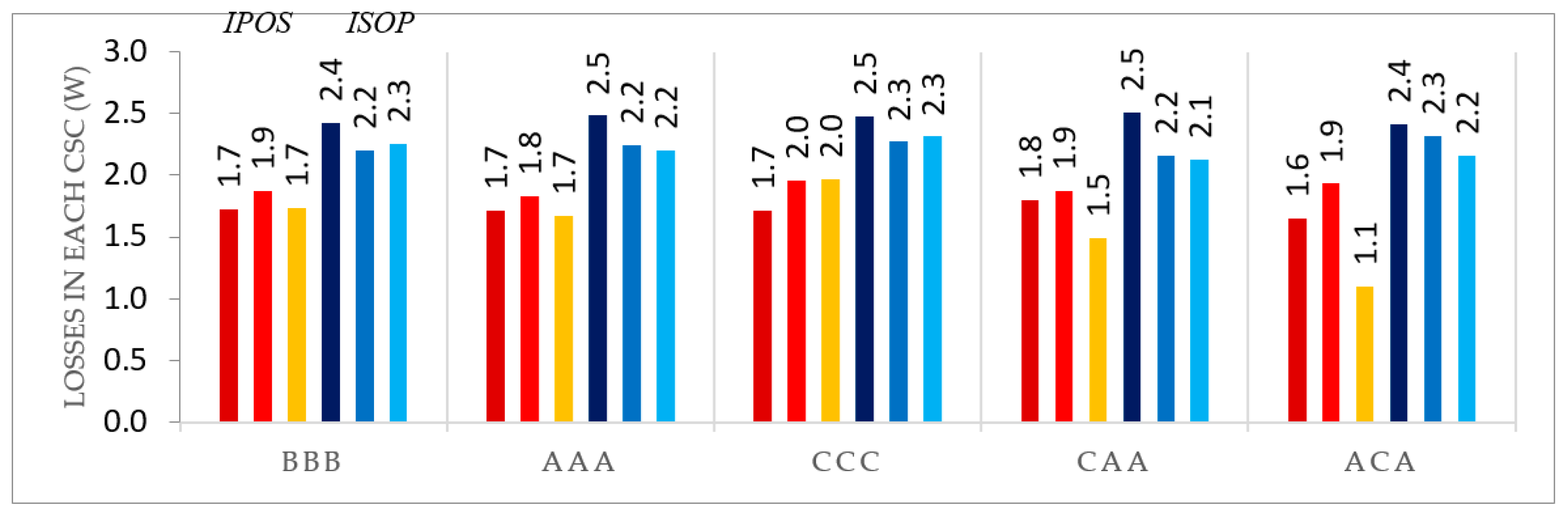
Figure 13 shows, with several graphs, the distribution of losses in each cell according to the arrangement for the IPOS and ISOP configurations. Red colors correspond to IPOS configuration whereas blue colors correspond to the ISOP configuration. For example, the first set of three bars in red colors in
Figure 13 represent the losses in each CSC for a configuration of 3 associated CSCs in IPOS.
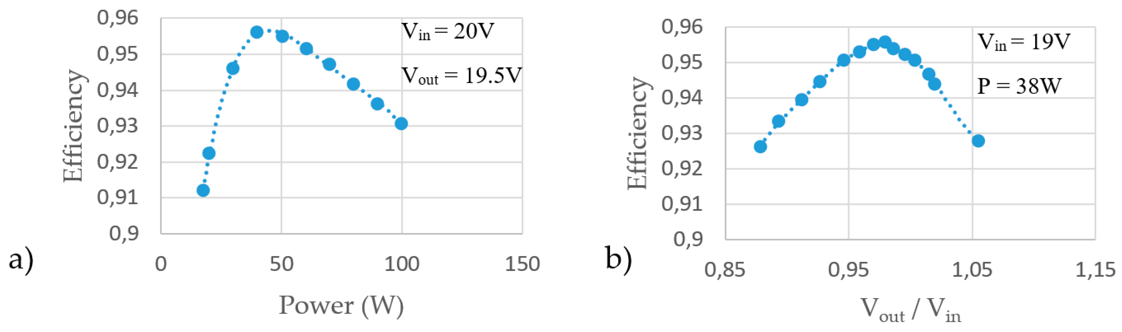
Overall, it is possible to see that losses are balanced as soon as the cells are from the same family while these losses are naturally more unbalanced in the case of a family mix. It is necessary to specify again that only one command is sent for the 3 CSCs and that the regulation is not done at the cell level. This imbalance is induced by output voltage variations which has a great impact on effiency and, therefore, losses as shown in
Figure 3.
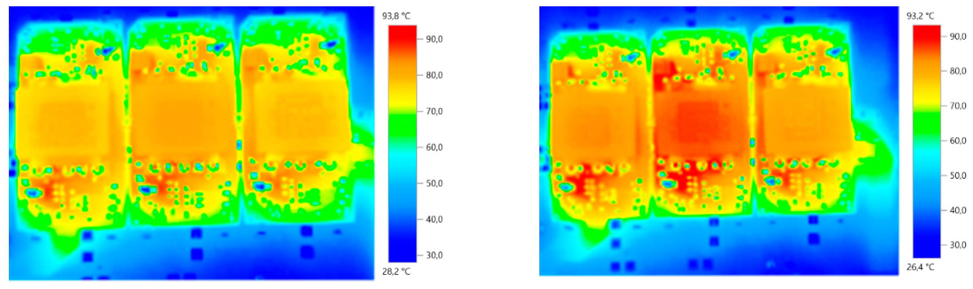
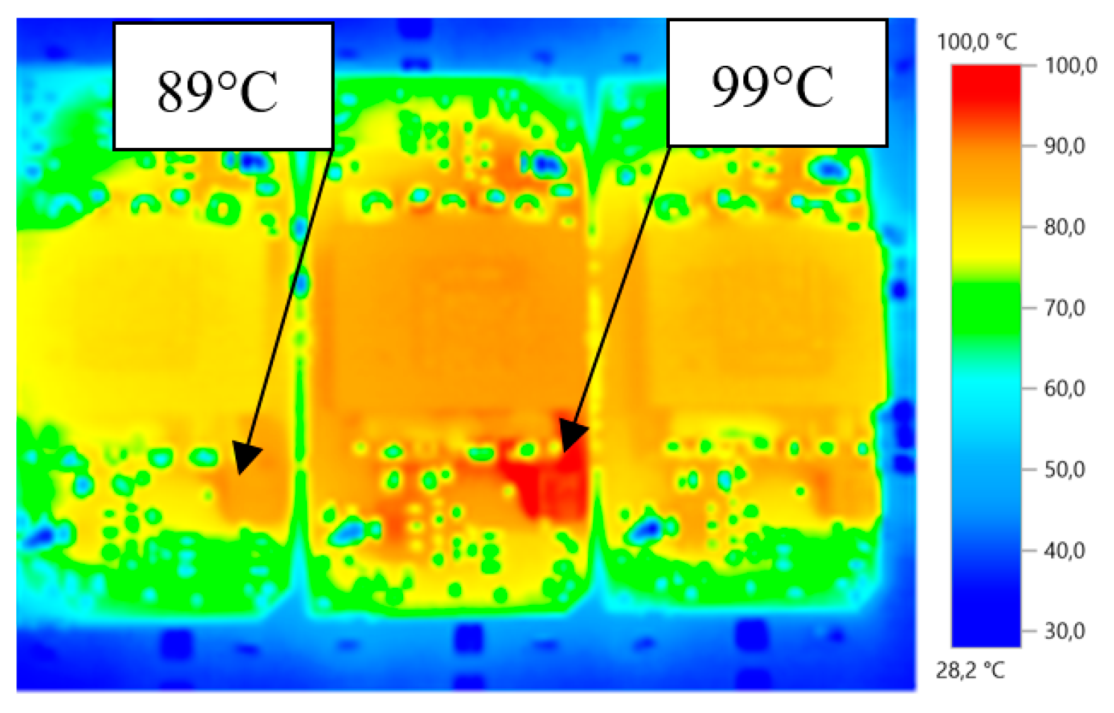
This deviation necessarily leads to a temperature rise that can be critical, as shown in the following thermal photos in
Figure 14.
On the thermal image above, a difference in the overall temperature of the cells according to their family is clearly visible. In
Figure 14, it is possible to measure up to 5 °C deviation over the same configuration if the cells are in extreme quintile (3 “C” CSCs or 3 “A” CSCs). For arrangements with mixed families, a more significant deviation can occur and bring a cell to a critical temperature as shown in
Figure 15. Some other arrangements and configurations which are not part of electrical Tests 1 and 2 presented in
Table 5 have showed that it can reach 10 °C deviation on two CSCs on the same PCA. This phenomenon is illustrated in
Figure 15. These observations should obviously be taken into consideration while designing the thermal cooling system.
4.3.3. Full Comparison of a PCA of CAA Family CSCs and a 5 CSCs ISOS Configuration
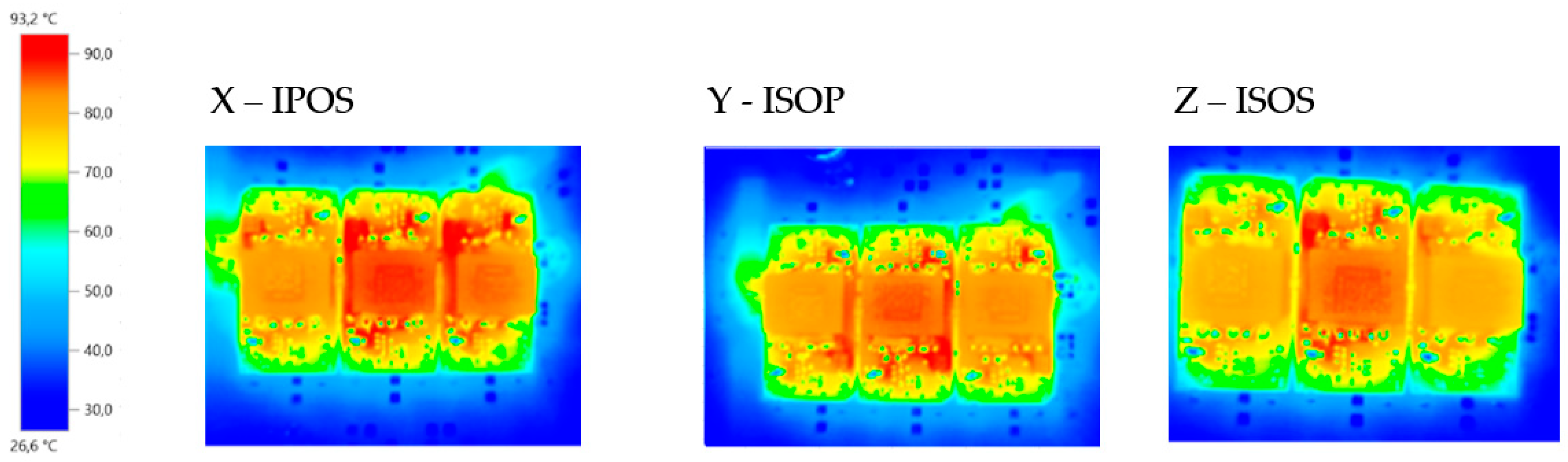
This part is investigating at first if three identical CSCs coming from a family mix may operate in a different manner depending on the configuration. The 3 CSCs are, from left to right, coming from family CAA. This choice is purely arbitrary, the goal being to see if there is a clear impact of the configuration on CSC behavior. The study provides, in
Table 6, for each configuration (IPOS/ISOP/ISOS) the operating point of each cell and
Figure 16, a thermal image of the PCA for each configuration.
These observations bring to light that ISOP configuration seems to be the worst case in terms of losses and efficiency. This result hides the important fact that CSCs operating points are significantly different due to absence of fixed voltage reference at the CSC input terminals. In such a way, CSCs are moving away from the optimal operating point, lowering their efficiency. This observation, which is valid for this case, may not always apply. Nonetheless, it shows that there are operating points that are leading to significant increase of losses.
Second, the ”weakest” CSC, understanding the cell with the lowest efficiency, remains the same no matter the configuration. This phenomenon is magnified due to the geographically positioned CSC in the middle always being warmer.
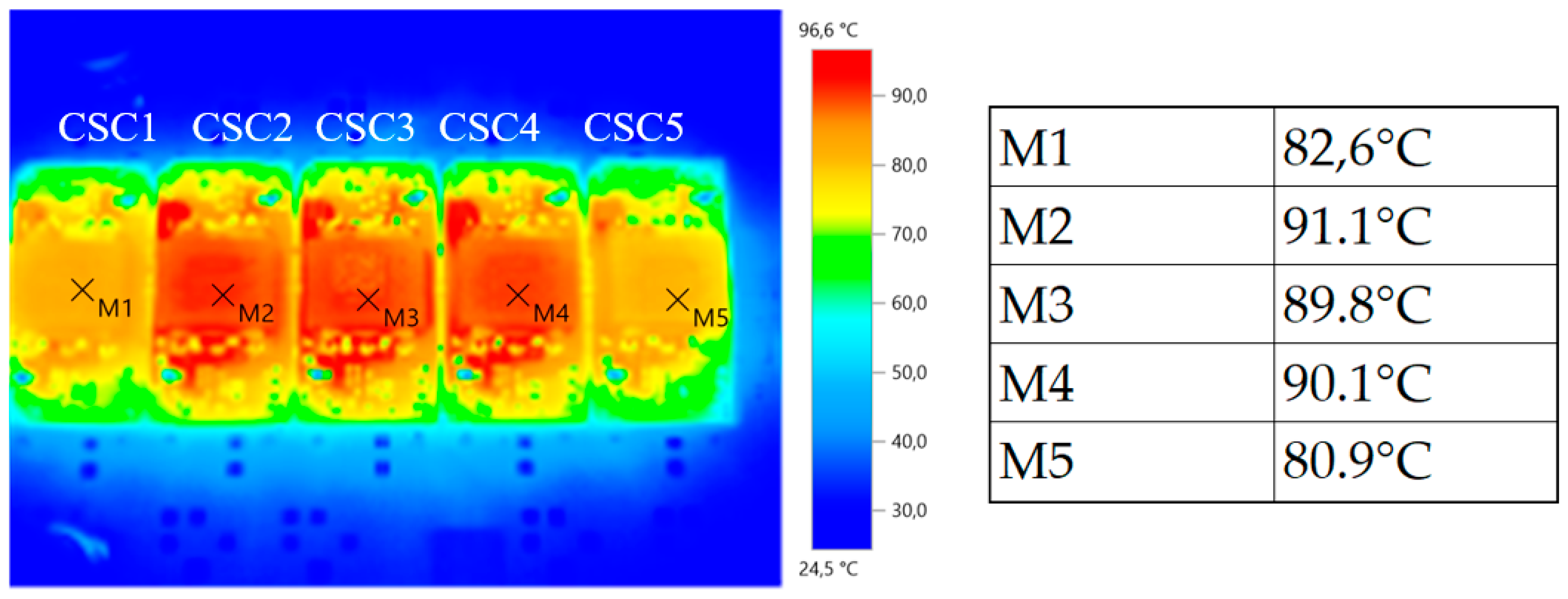
A second study shows a case study with 5 CSCs in ISOS configuration only. Until now, there were no results for 5 CSCs.
Table 7 shows the voltage and current distributions by cell for the following arbitrary family arrangement from left to right: BBCBA. This arrangement is representative of reality because, as shown in
Figure 5, there are few CSCs in family C and A which are coming from the extreme quintiles.
Several things can be noticed in
Table 7 and
Figure 17. The voltages of the first two CSCs (CSC1 and CSC2) of the B family are stable. CSC4 of family B does not have the same set of tensions This phenomenon is still under investigation. CSCs C and A have higher and lower voltages, respectively, than the tests done in the previous parts. On the thermal part, we notice that the external CSCs benefit from a lower temperature due to their peripheral placement. CSC2, CSC3 and CSC4 have the same temperature as shown in
Figure 1 while they have a different electrical operating point as shown in
Table 7. It can therefore be concluded that the disparity of the components during the ISOS configuration is smoothed at the thermal level but remains strong at the electrical level. Despite the differences in the electrical operating points of the CSCs, thermal images allow us to conclude that the placement of the CSC has a significant influence on its thermal equilibrium point. Nonetheless,
Figure 17 that the CSCs dispersion remains visible since the CSC at the middle of the array is colder than its direct neighbors. A relative impact of CSCs dispersion versus their physical position in the array could be considered in a future work.
4.4. Discussion of Main Results
Regarding the CSC batch characterization, it is important to highlight a few observations:
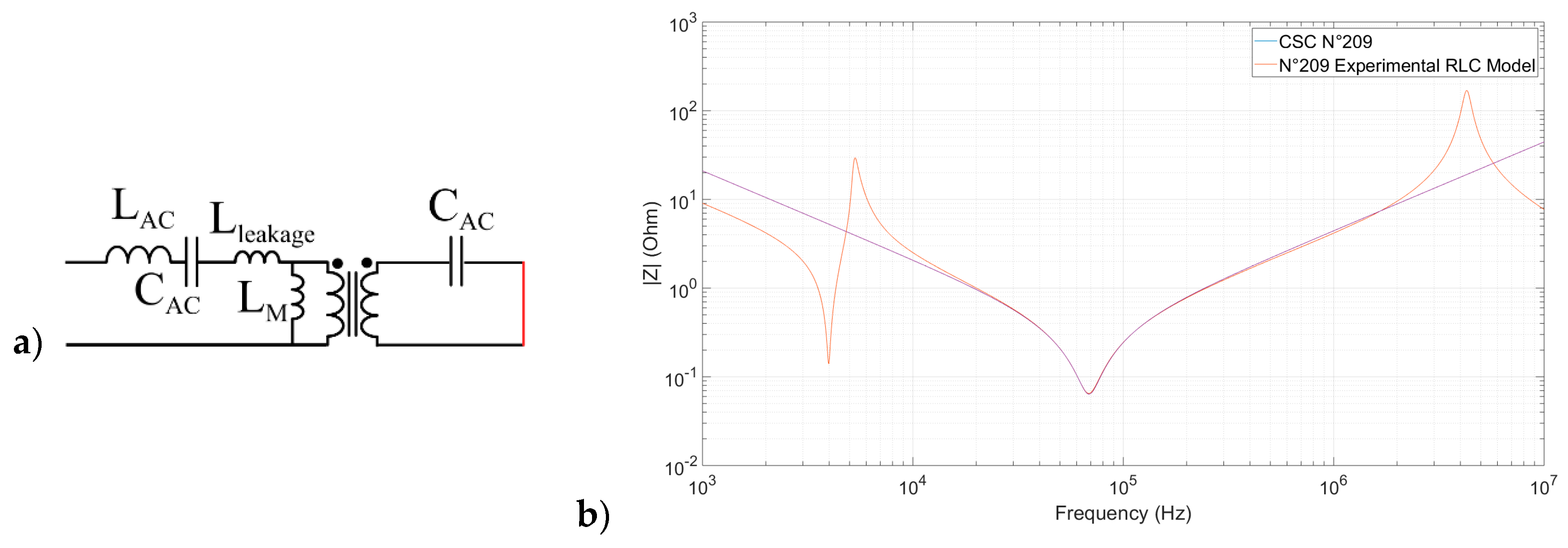
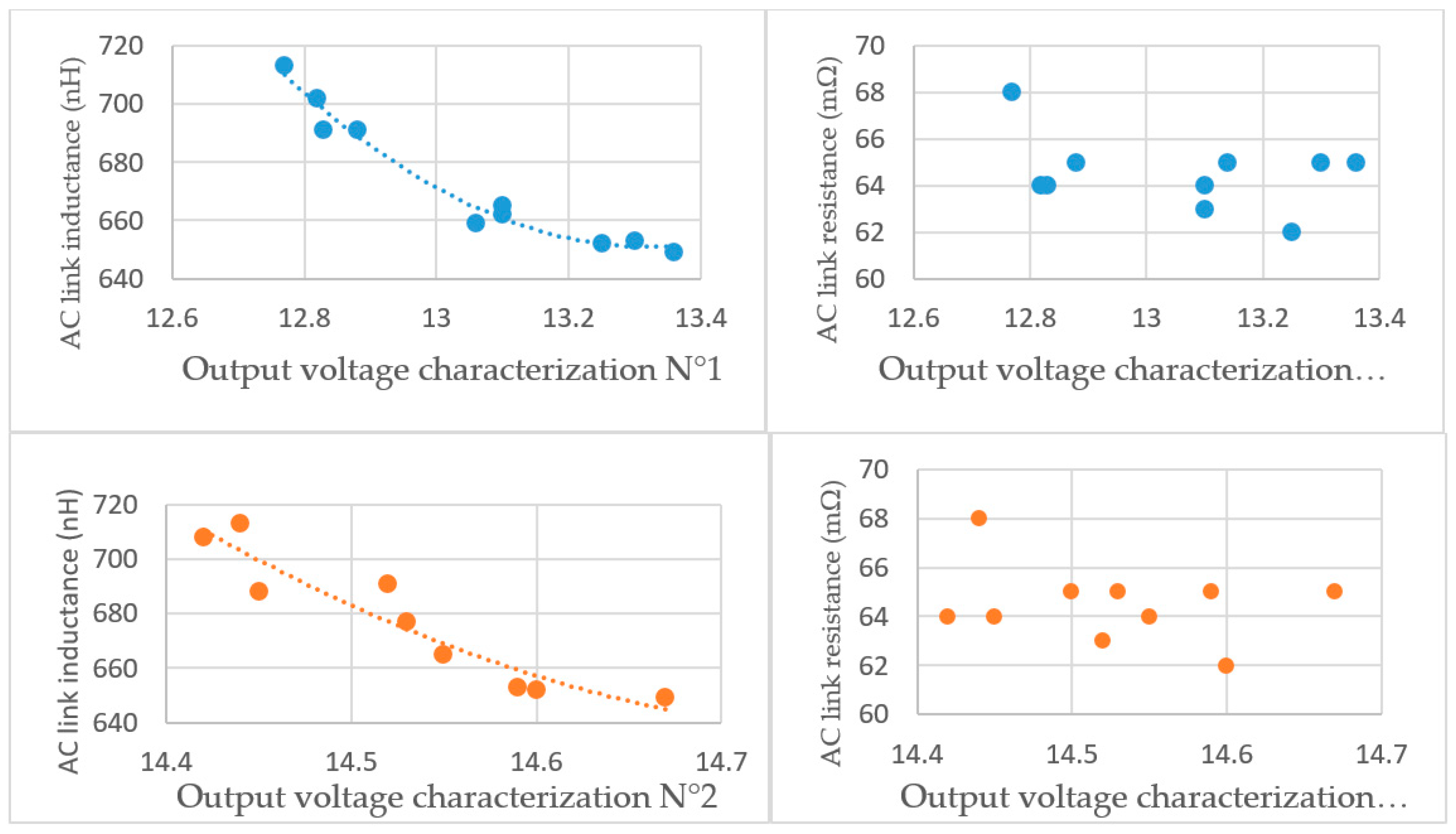
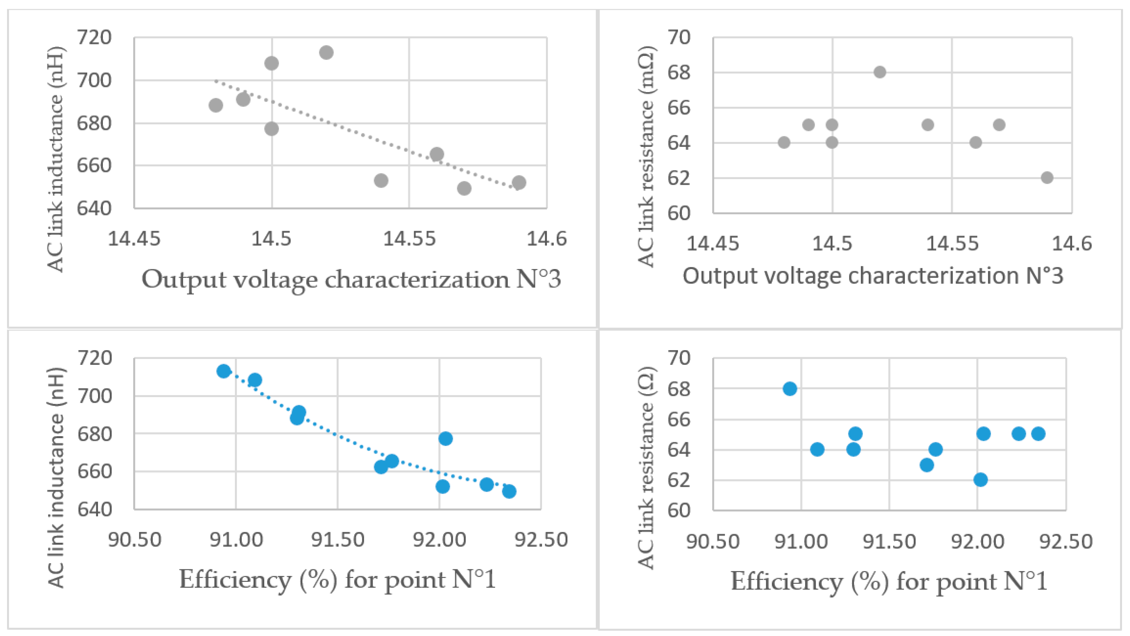
First of all, manufactured after a significant industrialization process, the CSCs remain slightly unpaired. This is mostly due to components that are provided by suppliers with tolerances. In our very specific example, CSCs are manufactured on PCBs and are all made out of off the shelf components with regular tolerances between 1% to 20%. Of course, the converter remains sensitive to the components’ main parameters. It appears, as a first result that the AC link inductor in DAB based topology is the most significant and critical component. Its sensitivity can be mathematically proven based on Equation (1). The tolerance on its value induces a tolerance on the whole DAB converter in terms of operating point, including CSC efficiency level. From that, it becomes important to frame the component tolerance such that it remains within good limits according to its application. In the case of the DAB converter, the tolerance on the total AC inductor introduces a large enough tolerance on the converter performances that it needs further investigations. Especially, in the presented case, CSCs being networked, it becomes critical to evaluate the impact of the converter operating point tolerance other an array of CSCs.
Regarding CSCs networks, some additional comments can be drawn:
Several CSC family arrangements have been implemented and characterized in three different configurations. ISOP, IPOS and ISOS were tested specifically because they are the three configuration for which a voltage unbalance among CSCs is possible either at the input or at the output terminals. These tests have been carried out at first in order to investigate how associations of CSCs with different voltage operating points would behave from that point of view. As a reminder, only an open loop was tested in this paper because closed loop control, although being impacted by cell imbalances, is not the purpose of this study.
Analyzing the results above, several comments can be made. First of all, the CSC operating point dispersion clearly affect the input and/or output voltage balance among cells. Paired CSCs have a more favorable behavior no matter the configuration. When arrangement involves CSCs from various families, their characteristic dispersion is mainly confirmed or even enhanced which may become an issue. Voltage imbalances induce efficiency unbalances. The total losses coming from the converter association are always higher than the sum of the losses gathered at cell levels for their expected operating point. This may have a significant impact on thermal management at the cell level.
In particular, it has been observed that in ISOP and ISOS configurations, the individual CSC behavior mismatches are enhanced by the network association. In fact, this is happening whenever the input voltage of the CSC is not fixed by the implementation. On the other side, IPOS configuration is very resilient to CSC characteristic tolerances.
From this analysis several options can be foreseen:
Provision must be taken while designing the thermal cooling. Considering the technology considered in this work, the PCB based CSCs are cooled down with air flow. With natural air cooling, CSCs’ current rating may have to be reduced to account for operating point variability and consecutive losses mismatches. With forced air cooling, increasing the air speed may compensate the losses mismatch among CSCs.
Since a functional testing is carried out after batch production, this test could include a short characterization of the meaning full operating point. The paper has clearly highlighted the relation between the component tolerance and their impact on converter operation and more specifically the output voltage with respect to all other parameter constant.
The functional test could be used to sort CSCs in quintile or even decile. In such a way, PCAs could be produced from paired CSCs, levering up voltage and current balancing among cells no matter the configuration.
The functional test could be used to remove CSCs that are too much out of a reasonable tolerance. For that, a good tradeoff between the tolerance window and the yield has to be found in order to remain reasonable from a cost point of view.
Figure 18 below presents an illustration of that process.
If sorting CSCs ends up to be too much unproductive or costly, another option is to work on the tolerance of the most critical components, probably the HF transformer and possibly the AC link additional inductor. Working on these two devices, sorting or selecting them could be a first option less costly than the whole CSC. Of course, this would require developing a test routine to sort components according to the leakage inductance for the HF transformer and the value of the inductor as far as the LAC inductor is concerned. Also, a specific work with the supplier could be carried at design and technological levels in order to narrow the tolerance on the components.


 ,
, 


