Abstract
In this paper, the principles of the open-loop frequency-based signal processing devices for capacitive MEMS accelerometers are used to develop three CMOS IP-core (Intellectual Property core) projects of highly sensitive signal processing devices with frequency output. Signal processing devices designed in accordance with the considered method form an output of rectangular pulses whose frequencies equal a difference of signal frequencies from two identical generators with micromechanical accelerometer capacitive transducers in their frequency control circuits. First, the analog project scheme uses two harmonic LC oscillators and an analog mixer to form an output rectangular-shape differential-frequency signal, the frequency of which is dependent on the measured acceleration. Second, the digital project is fully scalable for various CMOS-technologies due to oscillators of rectangular pulses and a digital mixer. Third, the mixed-signal project combines the advantages of the analog and digital projects. The signal processing device projects were developed, modeled and compared to comprehensively solve the problems of increasing sensitivity, dynamic range, noise immunity and resistance to destabilizing factors (e.g., to temperature changes).
1. Introduction
Present-day micromechanical accelerometers are widely used in different types of transport and electronic means from aerospace, water and auto transport systems to mobile phones and new generation video game consoles [1,2,3,4,5,6]. There are many kinds of transducers in present micromechanical accelerometers, such as capacitive, piezo-resistive, electromagnetic, optical, thermal convective, acoustic waves resonant, field emission, tunnel transducers and so on [6]. The micromechanical accelerometers with capacitive transducers are widely used due to relatively simple transducer structure, high-sensitivity, reliability, thermal stability, excellent linearity, resolution, bandwidth, good compatibility with integrated circuits technology, and consequently low cost [7,8,9,10,11,12,13,14].
Together with the transducers, the important functional blocks of micromechanical accelerometers are primary signal processing devices, which vastly determine characteristics of the sensory microsystems for motion parameters registration [14,15,16,17,18,19]. In capacitive accelerometers, the relative simplicity of a transducer’s construction and technology requires relatively complex signal processing devices for accurate measuring the nanoscopic changes of the proof mass position in capacitive transducers. As a result, capacitive accelerometers are more complex in comparison to many other sensors, e.g., resistive strain gauges [16].
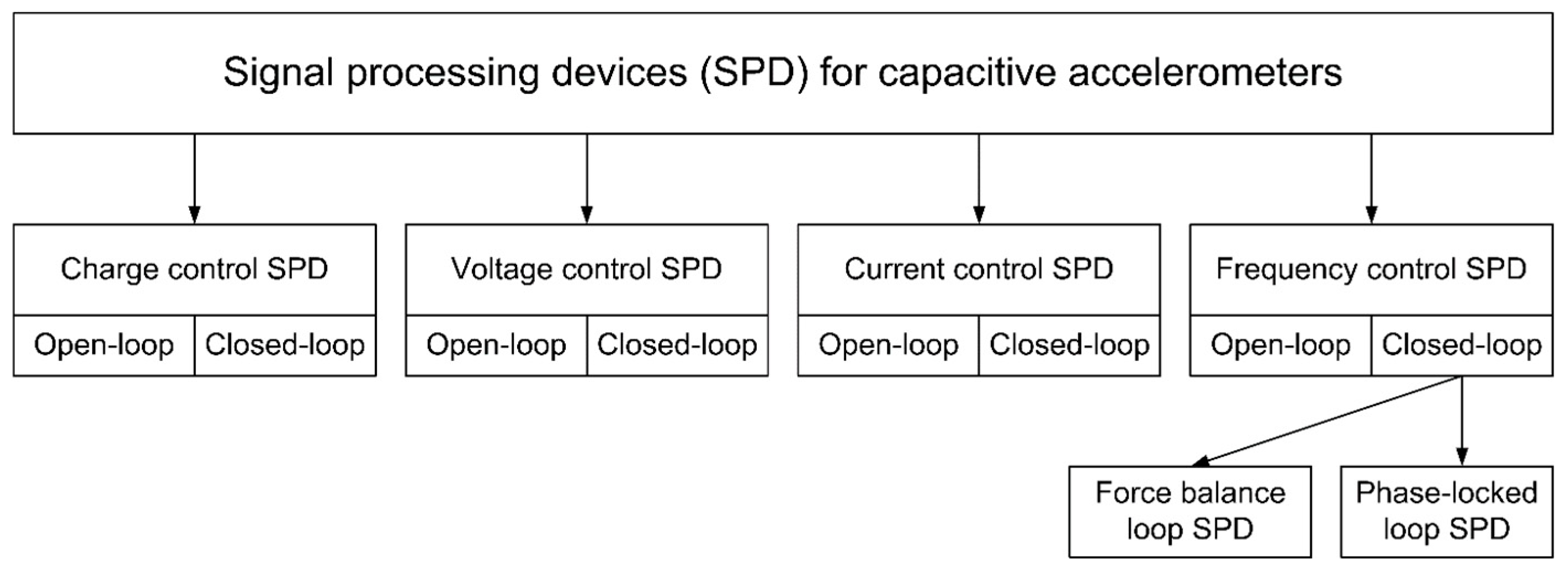
In the capacitive transducers, the nanoscopic displacement of the proof mass and corresponding capacity change induced by acceleration can be measured by detecting a change of charge, voltage, electric current, or frequency of an oscillator with the capacitive transducer in its frequency control circuit [19]. Figure 1 shows corresponding types of signal processing devices (SPD) for micromechanical capacitive accelerometers. Every type of SPD can be performed in both open-loop or closed-loop applications. Additionally, there are two variants of closed-loop SPD with frequency output: force balance loop and phase-locked loop [19]. Capacitive accelerometers with voltage control closed-loop signal processing devices are characterized by higher linearity and wider dynamic range in comparison with open-loop analogs. Moreover, the switching-capacitor charge-based technique is conventionally used in closed-loop SPD to effectively suppress flicker noise [19]. Therefore, voltage control closed-loop SPD are frequently used today especially for high-sensitivity and high accuracy MEMS accelerometers [8,9,10,11,12,13].
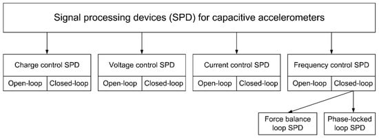
Figure 1.
Types of signal processing devices (SPD) for micromechanical capacitive accelerometers.
However, there are the following disadvantages of voltage control closed-loop signal processing devices:
- Necessity of comparatively power-hungry high-gain low-noise operational amplifier to minimize a noise floor of the MEMS accelerometer and increase its’ sensitivity [19];
- Influence of the operational amplifier’s thermal instability on the accuracy of the MEMS accelerometer [10];
- The offset of high-gain amplifier can saturate the output SPD voltage [20];
- Relative complexity of switching-capacitor closed-loop signal processing devices for accurately measuring the nanoscopic changes of the proof mass position in capacitive transducers [16];
- Scalability complication of switching-capacitor closed-loop SPD integrated implementation for the next technology generations.
This work is devoted to a comprehensive solution of aforementioned problems by means of development and comparative analysis of three IP-core projects of highly sensitive open-loop signal processing devices with frequency output for capacitive MEMS accelerometers. The first is an analog scheme SPD project based on harmonic LC or RC oscillators considered in Section 3. The second one is a well scalable fully digital scheme SPD project discussed in Section 4. The third project is a mixed-signal SPD investigated in Section 5. The common principles of the open-loop frequency control signal processing devices for the capacitive MEMS accelerometers are considered in Section 2. Section 6 presents the results of comparative analysis of the proposed SPD projects.
2. Common Principles of the Open-Loop Frequency Control Signal Processing Devices for Capacitive MEMS Accelerometers
2.1. Basic Differential Scheme of the Open-Loop Frequency-Based SPD for Capacitive MEMS Accelerometers
The basic principle of frequency control signal processing devices for capacitive MEMS accelerometers is a registration of acceleration induced change of transducer’s capacitance by means of including this capacitance in the frequency control circuit of oscillator and measuring corresponding change of the output frequency [18,19].
According to Figure 1 the frequency-based SPD can be implemented in closed-loop or open-loop approaches. Closed-loop frequency-based SPDs require frequency-to-voltage conversion for the force-balance loop or phase-to-voltage conversion for the phase-locked loop. Therefore, closed-loop frequency-based SPDs conventionally include such functional modules as operational high-gain low-noise amplifiers, digital-to-analog and analog-to-digital converters (DAC and ADC, respectively), active low pass filters and so on [19]. Accordingly, this complication and other aforementioned disadvantages of closed-loop frequency-based technique is similar to the features of the closed-loop voltage-based SPD.
In contrast to this, open-loop frequency-based SPD is free of DAC, ADC and operational amplifiers and consequently it is extremely more convenient for integrated MEMS implementation than closed-loop approach.
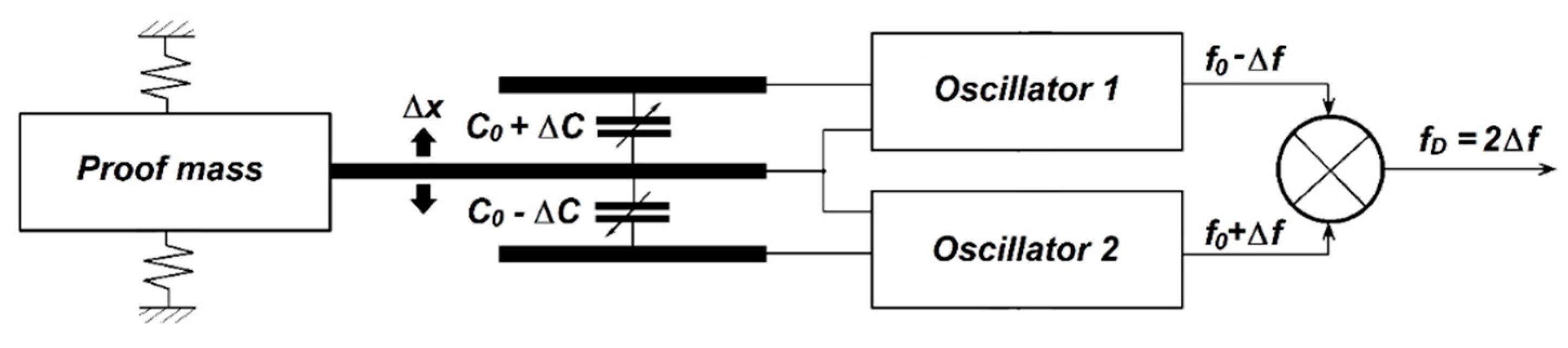
To increase sensitivity and thermal stability of frequency-based SPD, the differential principle of output frequency synthesis is conventionally used [2,19]. This principle is schematically shown in Figure 2.
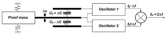
Figure 2.
Differential principle of frequency-based signal processing devices for capacitive MEMS accelerometers.
2.2. Output Differential Frequency and Sensitivity of the Frequency-Based Accelerometers
According to the differential principle, a frequency-based signal processing device contains two identical oscillators (Oscillator 1 and Oscillator 2 in Figure 2) with differential sensing capacitors in the frequency control circuits. In the initial state without acceleration, the capacitances of the both first and second sensing capacitors equal C0, the frequencies of the Oscillator 1 and Oscillator 2 equal f0, and frequency difference fD on the mixer’s output is defined by phase noise and jitters of the oscillators only. Under the acceleration ax, the displacement Δx of the proof mass provides corresponding changes of sensing capacitances C0 + ΔC, C0 − ΔC, and oscillator frequencies f0 + Δf, f0 − Δf. As a result, the output differential frequency fD is defined by:
where Δf is the acceleration induced change of oscillator frequency.
fD = 2⋅Δf,
The output frequency difference, fD, for RC oscillators can be expressed as a function of acceleration induced changes of sensing capacitances C0 + ΔC, C0 − ΔC:
where R is a resistance of the RC oscillator frequency control circuits; Cp is a parasitic capacitance.
fD = 1/[2πR(Cp + C0 − ΔC)] − 1/[2πR(Cp + C0 + ΔC)] = 1/(2πR) ⋅ 2ΔC/[(C0 + Cp)2 − ΔC2],
Conventionally for capacitive transducers:
ΔC << C0 + Cp.
Taking into account Equation (3), Equation (2) can be rewritten as:
where frequency of oscillators without acceleration f0 is defined by
fD ≈ 1/(2πR) ⋅ 2ΔC/(C0 + Cp)2 = 1/[2πR(C0 + Cp)] ⋅ 2ΔC/(C0 + Cp) = 2f0 ⋅ ΔC/(C0 + Cp),
f0 = [2πR(C0 + Cp)]−1.
Approximate Equation (4) can also be obtained for the difference frequency, fD, of LC generators with following equation for f0:
where L is an inductance of the LC oscillator’s frequency control circuits [19].
f0 = (2π)−1 ⋅ [L(C0 + Cp)]−1/2,
A change of sensing capacitance ΔC is expressed through a displacement Δx of the proof mass as follows:
where ε0 is the vacuum permittivity; S is a square of sensing capacitor; d0 is a distance between the electrodes of the sensing capacitor without acceleration.
2ΔC = ε0S/(d0 − Δx) − ε0S/(d0 + Δx) = ε0S ⋅ 2Δx/(d02 − Δx2),
Taking into account that Δx << d0 and that sensing capacitance without acceleration C0 = ε0S/d0, we can rewrite Equation (7) as follows:
2ΔC = 2ε0S/d0 ⋅ Δx⋅d0/(d02 − Δx2) ≈ 2C0 ⋅ Δx/d0.
The displacement Δx of the proof mass is defined by the measured acceleration ax:
where mx is the proof mass; kx is a stiffness of the proof mass spring; ωr is a resonant frequency of the micromechanical transducer.
Δx = mx/kx ⋅ ax = ax/ωr2,
Substituting Equations (8) and (9), Equation (4) can be rewritten as follows:
fD(ax) ≈ f0 ⋅ 2C0/(C0 + Cp) ⋅ mx⋅ax/(kx⋅d0) = f0 ⋅ 2C0/(C0 + Cp) ⋅ ax/(ωr2⋅d0).
Correspondently the sensitivity of the frequency-based accelerometer is defined by the equation:
dfD/dax ≈ f0 ⋅ 2C0/(C0 + Cp) ⋅ mx/(kx⋅d0) = f0 ⋅ 2C0/(C0 + Cp) ⋅ 1/(ωr2⋅d0).
According to Equations (10) and (11), the output frequency and the sensitivity of the frequency-based MEMS accelerometer are determined by the initial frequency of the oscillators, f0. Oscillator frequencies in modern integrated circuits can reach tens of GHz. Therefore, the sensitivity of the frequency-based accelerometers can be selected in a wider range than the sensitivity of the accelerometers with voltage output, which is limited by the gain of amplifier and power voltage. At the same time, the scheme of the frequency-based SPD presented in Figure 2 is much simpler than schemes of voltage-based signal processing devices of the capacitive MEMS accelerometers [16]. Moreover, the offset of high-gain amplifiers in voltage-based accelerometers may saturate the output SPD voltage [20]. The frequency-based high sensitivity accelerometers are free from this drawback.
2.3. Resistance of the Open-Loop Frequency-Based SPD to Destabilizing Factors
Another important advantage of the frequency-based signal processing devices is a resistance to destabilizing factors, such as temperature, due to differential principle of output signal synthesis. Temperature induced changes of the frequencies of two identical oscillators (Oscillators 1 and 2 in Figure 2) are mutually compensated in the mixer when the output differential frequency signal is formed.
2.4. Noise Floor and Dynamic Range of the Frequency-Based Accelerometers
A most important aspect of designing of the signal processing devices for capacitive MEMS accelerometers is a noise-floor, which defines threshold sensitivity and dynamic range of the accelerometer. The dynamic range RD in dB is described by:
where Smax is a maximum level of measured signal; NRMS is a noise-floor RMS.
RD = 20 ⋅ lg(Smax/NRMS),
In the case of the considered frequency-based SPD, the maximum level of measured signal corresponds to maximum output differential frequency, fDmax, and NRMS corresponds to a phase noise RMS of the oscillators, ΔfRMS:
RD = 20 ⋅ lg(fDmax/ΔfRMS).
A noise-floor RMS of the capacitive accelerometers is defined by two components:
- A primary mechanical noise of sensing capacitors defined by the Brownian motion of the proof mass due to Brownian motion of the surrounding gas molecules [6];
- An intrinsic noise of signal processing devices of MEMS accelerometers.
A primary mechanical noise of sensing capacitors is manifested as the voltage fluctuations on the high-gain amplifier input in voltage-based or charge-based SPD, and as the frequency fluctuation (phase-noise) in the outputs of the oscillators and mixer in a frequency-based SPD. In the voltage-based or charge-based SPD, these voltage fluctuations are significantly amplified by the high-gain amplifier. This requires an increase of the proof mass to minimize the noise-floor and expand the dynamic range RD [7,8,13]. In contrast to this, there is no amplifier in the open-loop frequency-based SPD (Figure 2). Therefore, on the one hand the noise amplitude is not amplified from input to output, and on the other hand the amplitude of the noise voltage does not affect the threshold sensitivity and dynamic range of the accelerometer because the informative parameter of output signal is not voltage level, but differential frequency fD.
The important stage of accelerometer signal processing is a post-processing stage. In the open-loop frequency-based SPD, post-processing does not require amplifiers, ADC and DAC. In these SPDs, only a digital counter is used for measuring output pulses’ period TD or output frequency fD = 1/TD.
When measuring the period TD, the digital counter counts a number of pulses of the high-stability clock oscillator during TD. The advantage of this approach is a high frequency of output data recounting (after each period of SPD output signal). At the same time, it needs a very high frequency clock oscillator with hundreds of times higher frequency than the difference frequency fD of the output signal, to provide a high accuracy of the period TD measurement. This may be a serious problem for a high-stability clock oscillator with quartz resonator. Herewith, a phase noise RMS on the SPD output will be comparatively high.
When measuring the frequency fD, the digital counter counts a number of SPD output signal pulses during the period of high-stability clock oscillator TCLK. The disadvantage of this approach is a comparatively low frequency of output data recounting (TCLK in this case must be the hundreds of times longer than period of SPD output signal to provide a high accuracy of the fD measurement). However, it is not a problem for modern frequency-based SPD because, as mentioned above, oscillator frequencies in modern integrated circuits can reach tens of GHz, which is several orders of magnitude higher than the bandwidth of the measured acceleration. Moreover, this approach allows significant suppression of phase noise levels during post-processing by averaging the output signal period TD on the period of high-stability clock oscillator TCLK.
2.5. Frequency Pulling Problem
One of the main problems of the differential scheme of open-loop frequency-based SPD presented in Figure 2 is the so called frequency pulling problem. This problem is manifested in the mutual pulling of the frequencies of two oscillators due to the coupling through the substrate, power-supply, common proof mass for sensing capacitors (Figure 2) and parasitic resistive, capacitive or inductive coupling between two oscillators [19,21,22].
To avoid frequency pulling problems some following techniques are used:
- Separation of power-supply stabilizers for the oscillators [22];
- Distancing of the oscillators on a chip [22];
- Usage of two electrically isolated parts of the proof mass [19];
- Time-interleaved operation of the oscillators [23];
- Usage of the oscillators with sufficiently large difference between initial frequencies [22].
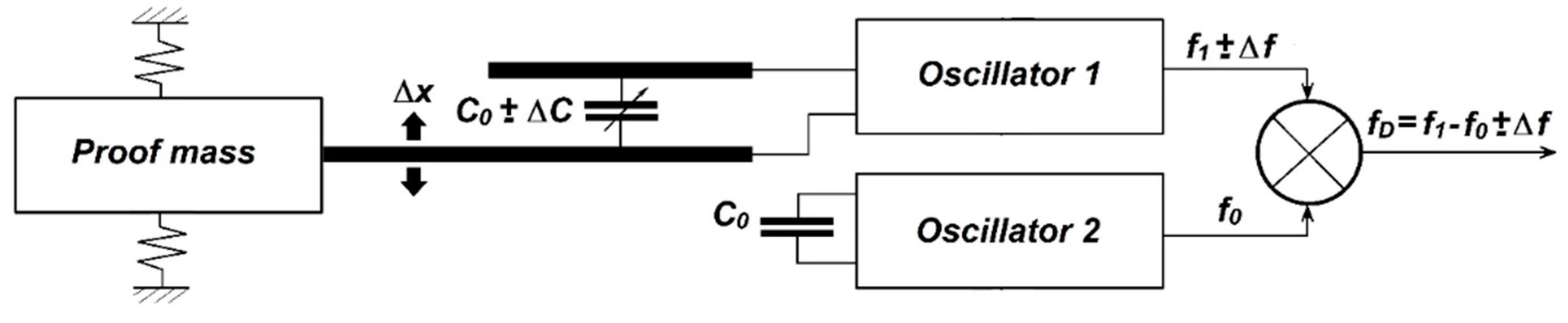
In this study, we consider the technique of frequency pulling problem solving based on the sufficiently large difference between initial frequencies of the oscillators in combination with the distancing of the oscillators on a chip and separation of power-supply stabilizers for the oscillators. Implementation of the considered technique is shown schematically in Figure 3.
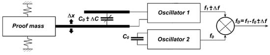
Figure 3.
Differential scheme of open-loop frequency-based SPD for frequency pulling problem solving.
In contrast to the basic principle of frequency-based SPD presented in Figure 2, in the scheme shown in Figure 3 capacitor sensitivity to acceleration is connected to the frequency control circuit of Oscillator 1 only. Output frequency f0 of the Oscillator 2 is not dependent on the measured acceleration. This approach completely deletes the coupling of the oscillators through the sensing capacitors and more effectively solves the frequency pulling problem by distancing the oscillators on a chip. In this case, it is enough to do the following:
- Topologically distance only the inductances of the oscillators to eliminate mutual induction;
- Implement two separate power pins for Oscillator 1 and Oscillator 2 for connection to separate stabilizers of power voltage.
Additionally, to avoid a frequency pulling, a difference between initial frequencies of Oscillator 1 and Oscillator 2 is introduced:
where fD0 is a differential frequency of output signal without acceleration (ax = 0); f1 and f0 are the initial frequencies of Oscillator 1 and Oscillator 2, respectively.
fD0 = f1 − f0,
Initial frequency f1 of Oscillator 1, which corresponds to the acceleration ax = 0, can be defined by as:
where Δfmax is a maximum acceleration induced changing of the frequency of Oscillator 1.
f1 ≥ f0 + Δfmax,
An additional advantage of the difference between initial frequencies of the oscillators is a definition of the acceleration’s direction (positive or negative) in accordance to the sign of the difference fD − fD0. The basic scheme in Figure 2 needs an additional functional block for this purpose.
Evidently a differential scheme of signal processing devices for capacitive accelerometers presented in Figure 3 may be implemented using different techniques: with LC or RC oscillators, with harmonic or rectangular signals of oscillators, and with analog or digital scheme of the mixer. In this study, we propose three open-loop frequency-based SPD IP-core projects, which are compatible with the CMOS integrated circuits (IC) technologies.
3. Analog Scheme of SPD Project
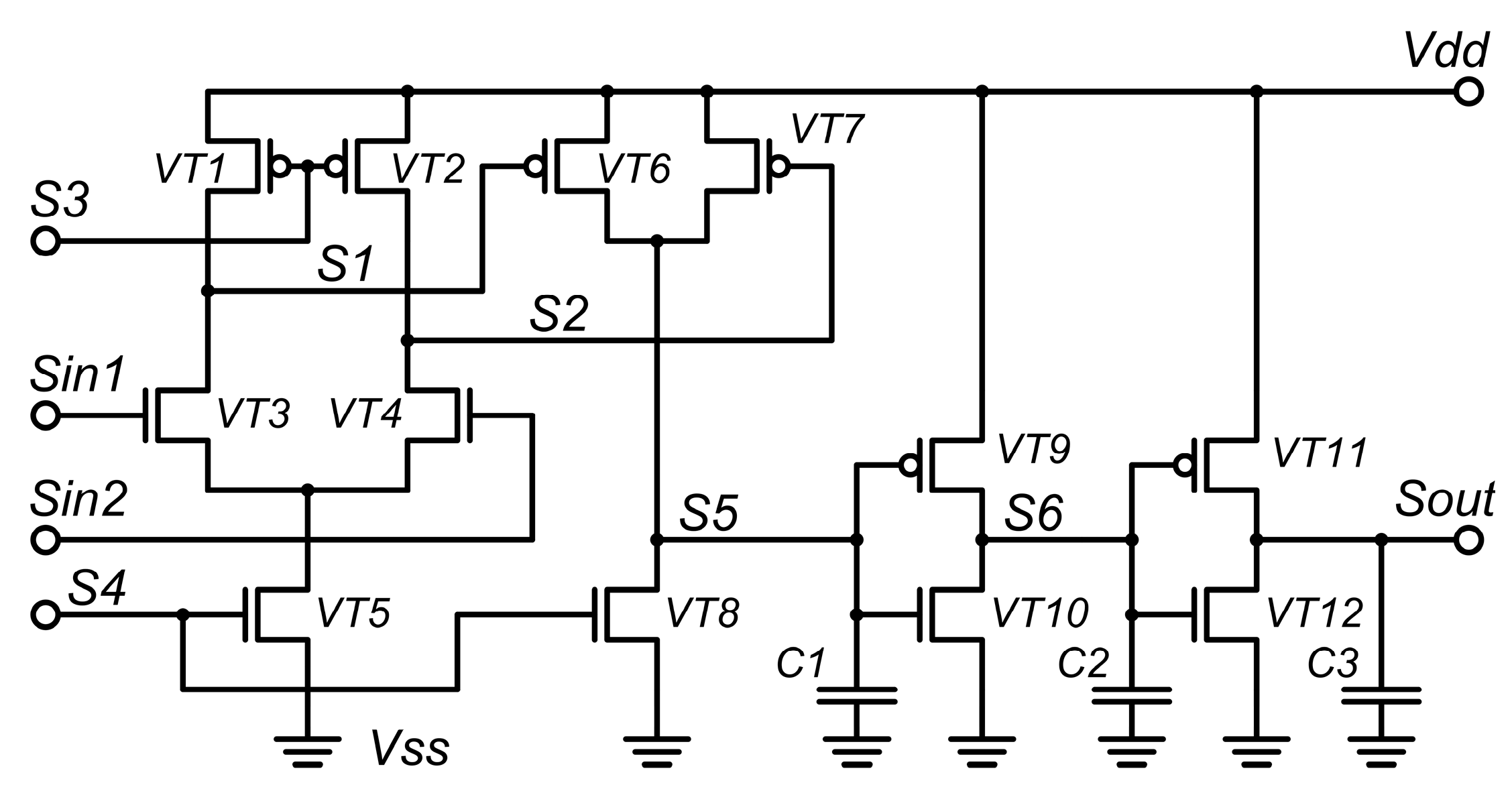
The first open-loop frequency-based SPD IP-core project used harmonic LC oscillators and CMOS analog scheme of the mixer. A scheme of this SPD project without oscillators is presented in Figure 4. The names and assignments of the SPD’s external signals are given in Table 1.

Figure 4.
CMOS analog scheme of open-loop frequency-based SPD project.

Table 1.
External signals of CMOS analog scheme of open-loop frequency-based SPD.
According to Figure 4, the proposed scheme contained the following functional blocks:
- Nonlinear differential cascade on the transistors VT1–5, which combine the functions of a mixer, rectifier and amplifier;
- Detector on the transistors VT6–8 and the capacitor C1;
- First comparator in the form of CMOS-inverter on the transistors VT9 and VT10;
- First low-pass filter on the capacitor C2;
- Second comparator in the form of CMOS-inverter on the transistors VT11 and VT12;
- Output low-pass filter on the capacitor C3.
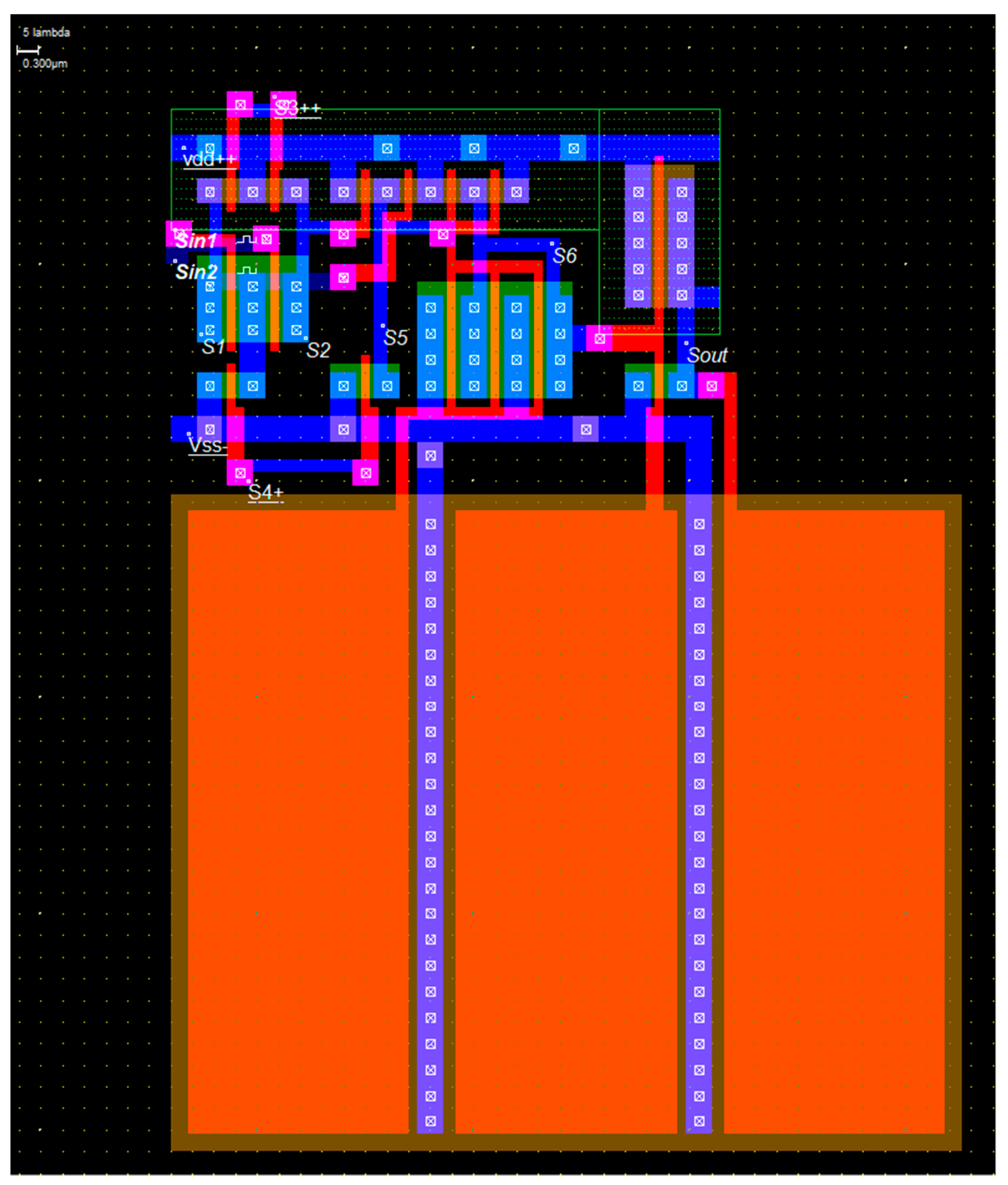
A layout of IC implementation of the analog frequency-based SPD scheme is presented in Figure 5. This project was implemented for CMOS 0.12 μm technology in layout editor of CAD Microwind [24].
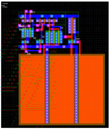
Figure 5.
A layout of CMOS analog open-loop frequency-based SPD.
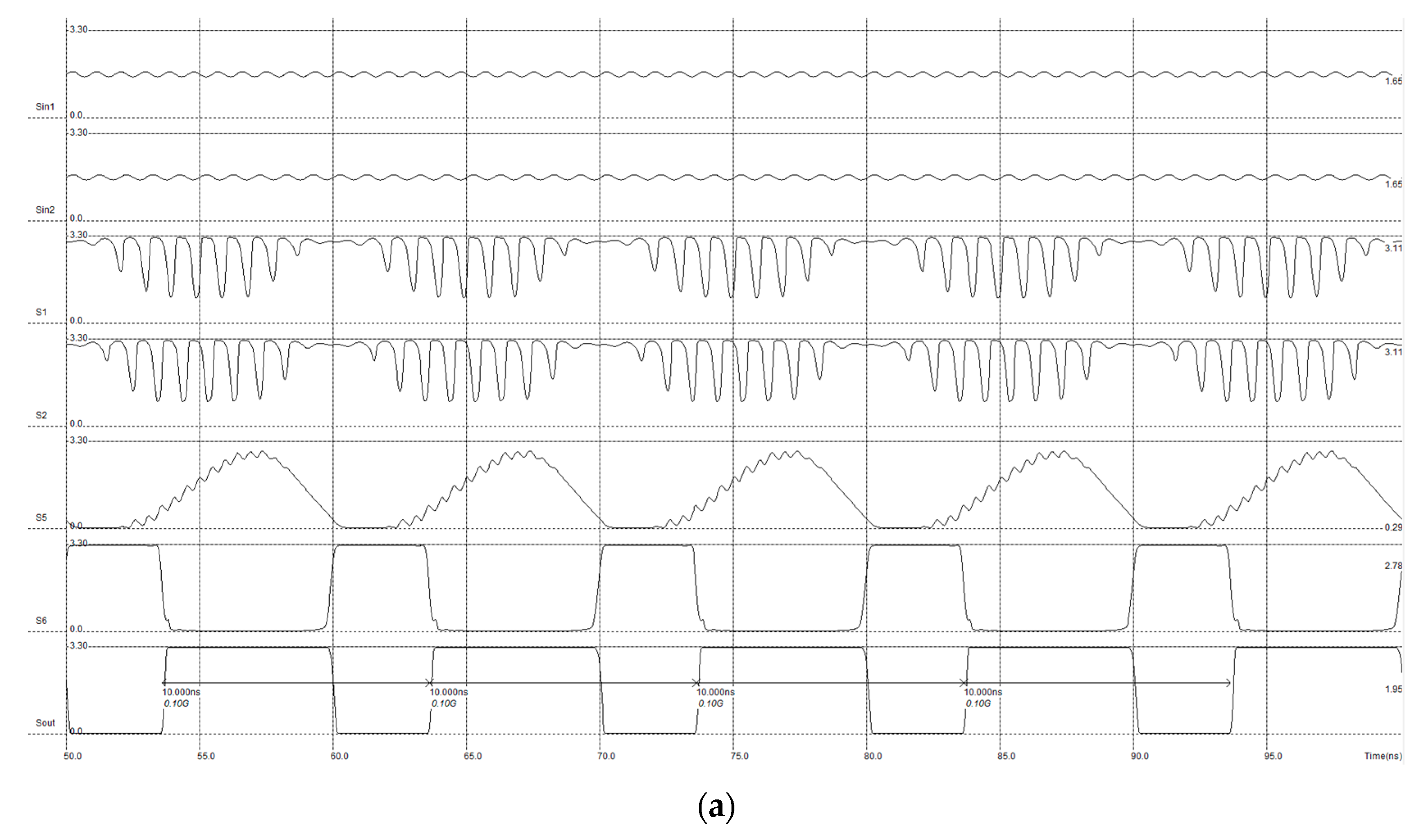
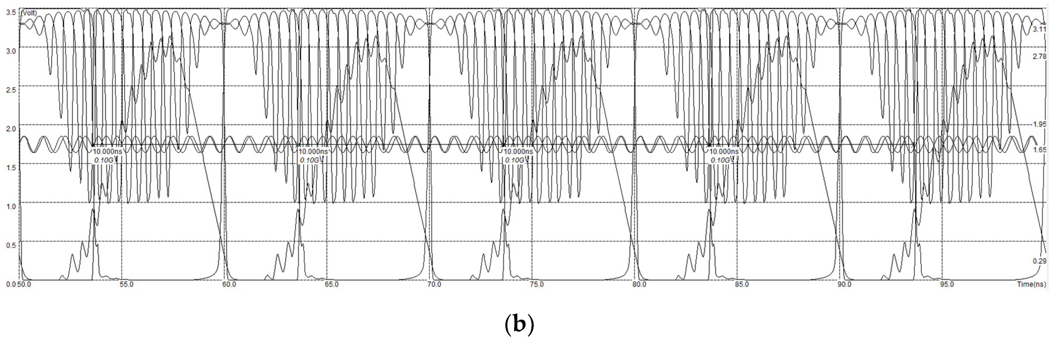
Results of electrical modeling of the analog frequency-based SPD project for initial conditions Δf = 0 and correspondent differential frequency fD = fD0 = 100 MHz are shown in Figure 6.
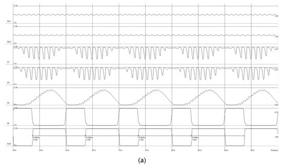

Figure 6.
Transients of the analog frequency-based SPD project in separated (a) and aligned (b) graphs for Δf = 0 and fD = fD0 = 100 MHz.
Basic parameters of the transistors and external signals of SPD are given in Table 2.
Table 2.
Basic parameters of the transistors and the external signals of CMOS analog frequency-based SPD.
Distinctive features of the CMOS scheme proposed in Figure 4 are:
- Functional block of nonlinear differential cascade on the transistors VT1–5;
- Functional block of detector on the transistors VT6–8.
According to the scheme of SPD in Figure 4, harmonic signals Sin1 and Sin2 of the oscillators were fed to the inputs of the differential cascade on the transistors VT1–5. Frequency of the signal Sin1 was dependent on the measured acceleration f1 ± Δf(ax). Frequency of the signal Sin2 was independent on the acceleration. The cascade operating point was calculated to provide a nonlinear mode of operation. In this mode, the differential cascade combined the functions of a mixer, a rectifier and an amplifier with a gain of 10 for the parameters of input signals (Sin1, Sin2) and offset voltages (S3, S4) given in Table 2.
As a result, according to transients in Figure 6, output signals of differential cascade S1 and S2 were amplified, rectified and modulated in amplitude with a frequency equal to the frequency difference fD of the input signals Sin1 and Sin2.
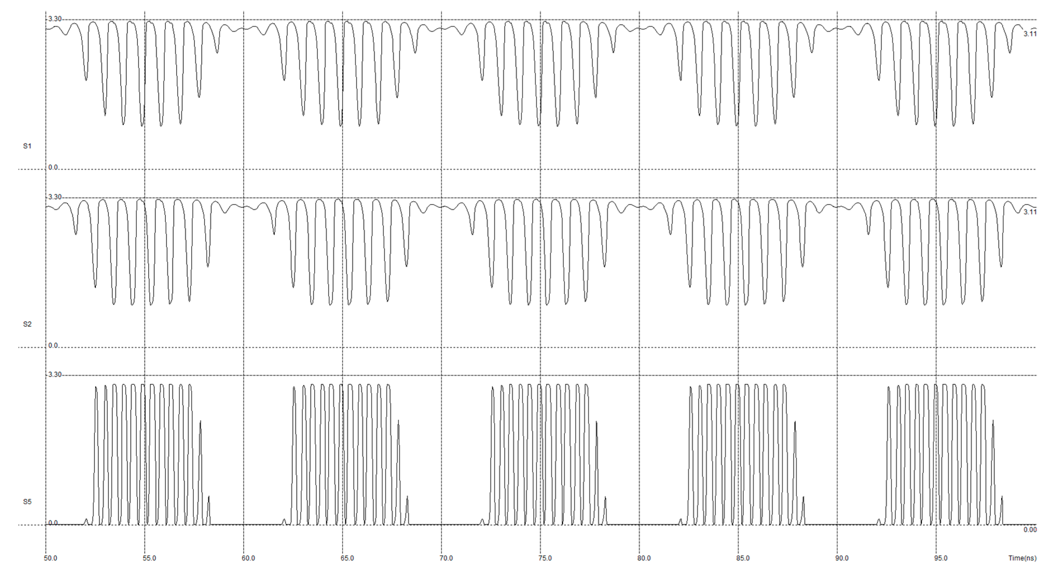
Next, the signals S1 and S2 were fed to the detector inputs on transistors VT6–8 and capacitor C1. Detector transistors provided a superposition, inversion and amplification of half-phases of the signals S1 and S2 in signal S5 in accordance to Figure 7. Transients of the detector in Figure 7 were simulated without capacitor C1, which suppressed the pulsation amplitude and selected a signal enveloping S5 with difference frequency fD shown in Figure 6.
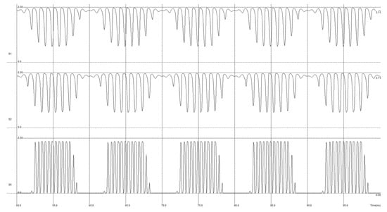
Figure 7.
Transients of the detector without capacitor C1.
One of the key design tasks of proposed signal processing device was a definition of the initial values of frequencies f0 and f1 in Table 2.
The minimum value of the frequency f0, independent of acceleration ax, was determined by the maximum allowable design area SLmax of the inductance L2 for the Oscillator 2 on the chip:
f0 ≥ (2π)−1 ⋅[L2(C0 + Cp)]−1/2.
The maximum value f1max of the frequency f1 of the Oscillator 1, corresponding to maximum positive acceleration axmax, was determined as follows:
where ftech is a maximum oscillator frequency defined by the CMOS technology used. We define ftech as the frequency at which the amplitude of the oscillator signal decreases by 3 dB relative to the maximum value.
f1max(axmax) ≤ ftech,
The minimum value f1min of the frequency f1 of the Oscillator 1, corresponding to maximum negative acceleration −axmax, is determined by expression:
where Kpull < 1 is an empirical coefficient defining the minimum ratio fDmin/f0 (where fDmin = f1min − f0) at which the pulling effect for oscillators is guaranteed to be impossible for the entire working temperature range. The value of Kpull should be experimentally measured for the CMOS technology used.
f1min(−axmax) ≥ (1 + Kpull) f0,
The initial value f1, corresponding to ax = 0, is determined as follows:
f1 = (f1max − f1min)/2.
Basic parameters of the transducer used for SPD modeling and for calculation of the frequencies f0 and f1 are given in Table 3.
Table 3.
Basic parameters of the transducer used for modeling.
Next, the signal S5 was fed to the input of series-connected comparators on transistors VT9–12 and low-pass filters on capacitors C2 and C3. CMOS-inverters were used as the comparators. This functional block transformed harmonic-like signal S5 in the rectangular output digital signal Sout with the same frequency fD. The capacitors C2 and C3 deleted undesirable pulsations in the output. Corresponding transients are shown in Figure 6.
Figure 8 shows the transients of the considered SPD project for the negative and positive accelerations, which induced output frequency changes Δf = −50 MHz (fD = 50 MHz in Figure 8a for negative direction of the acceleration) and Δf = 50 MHz (fD = 150 MHz in Figure 8b for positive direction of the acceleration).
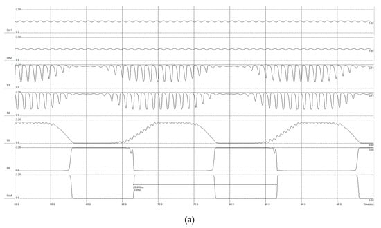
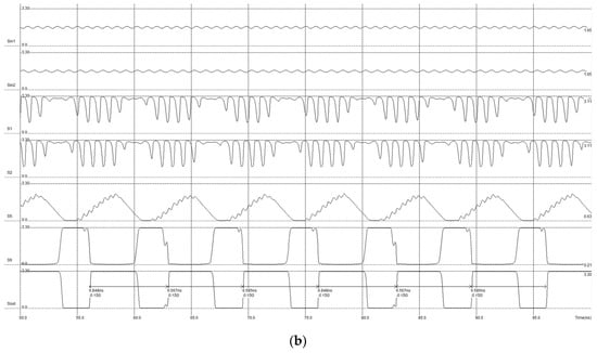
Figure 8.
Transients of the analog frequency-based SPD project for negative (Δf = −50 MHz and fD = 50 MHz (a)) and positive (Δf = 50 MHz and fD = 150 MHz (b)) directions of measured acceleration.
To illustrate a noise immunity of the considered SPD, transients for noised signals of the oscillators Sin1 and Sin2 with an RMS noise NRMS = 0.5 V are shown in Figure 9.
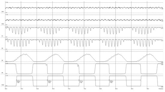
Figure 9.
Transients of the analog frequency-based SPD project for initial conditions (Δf = 0 and fD = fD0 = 100 MHz) and for noised input signals S1 and S2 with RMS noise NRMS = 0.5 V.
According to Figure 9, an excellent functionality of the considered frequency-based SPD was saved even for RMS noise of input signals S1 and S2 (NRMS = 0.5 V) higher than amplitude of these signals (0.1 V). However, noise of input signals increased a jitter Jout of output signal Sout in comparison with the transients of Sout without input noise in Figure 6. Considering a jitter Jout of digital output signal as a maximum time interval between corresponding rising fronts of Sout taking into account input noise (in Figure 9) and ideal condition (without input noise in Figure 6) we got a value Jout = 0.41 ns, which was 4.1% of the period of ideal Sout (Tout = 10 ns in Figure 6). It should be noted, that real RMS of input signals noise may be considerably lower than an amplitude of these signals (in the considered project, 0.1 V). In this case, output jitter will be considerably lower too.
An important advantage of the considered SPD project is a possibility of increasing the frequency of the oscillators to maximum values determined by the CMOS-technology used and the permissible level of phase noise. According to Equations (11) and (13), higher frequency of the SPD oscillators provides an increase in sensitivity and dynamic range of the accelerometer.
However, a drawback of the developed SPD project is a bad scalability when the changing of CMOS-technology is needed. In this case, a full complex of project calculations and modeling is needed to provide a good functionality and necessary values of the parameters.
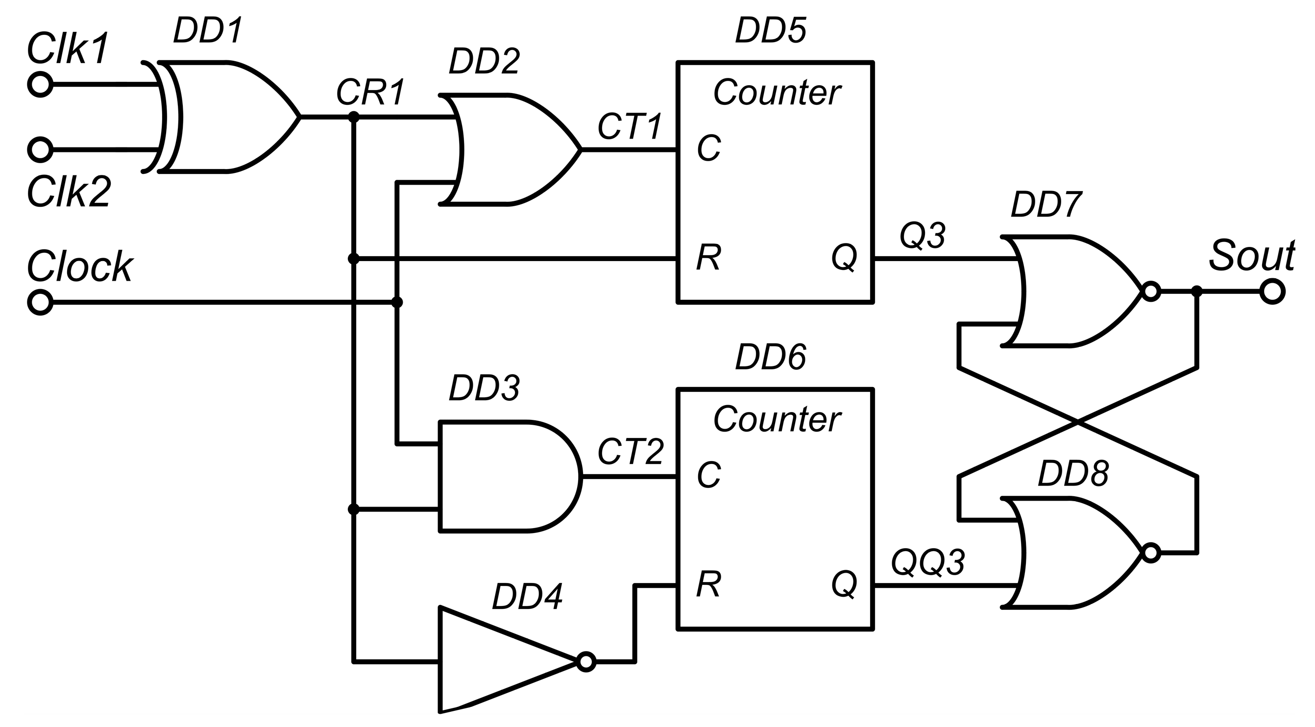
4. Fully Digital Scheme of SPD Project
The second IP-core project of open-loop frequency-based SPD used oscillators of digital rectangular pulses and a fully digital CMOS-scheme of the mixer. A scheme of this SPD project without oscillators is presented in Figure 10. The names and assignments of SPD’s external signals are given in Table 4.
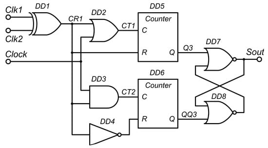
Figure 10.
Fully digital CMOS-scheme of open-loop frequency-based SPD project.
Table 4.
External signals of fully digital CMOS-scheme of open-loop frequency-based SPD.
According to Figure 10, the proposed scheme contains the following functional blocks:
- Digital mixer of rectangular input signals Clk1 and Clk2 on the XOR logic element DD1;
- Functional block for determination of the duration of the mixer’s output pulses on the logic elements AND (DD3) and NOT (DD4), and on the digital counter DD6;
- Functional block for determination of the intervals between mixer output pulses on the logic elements OR (DD2) and the digital counter DD5;
- RS-trigger on the logic elements NOR (DD7, DD8) for differential-frequency output signal Sout synthesis.
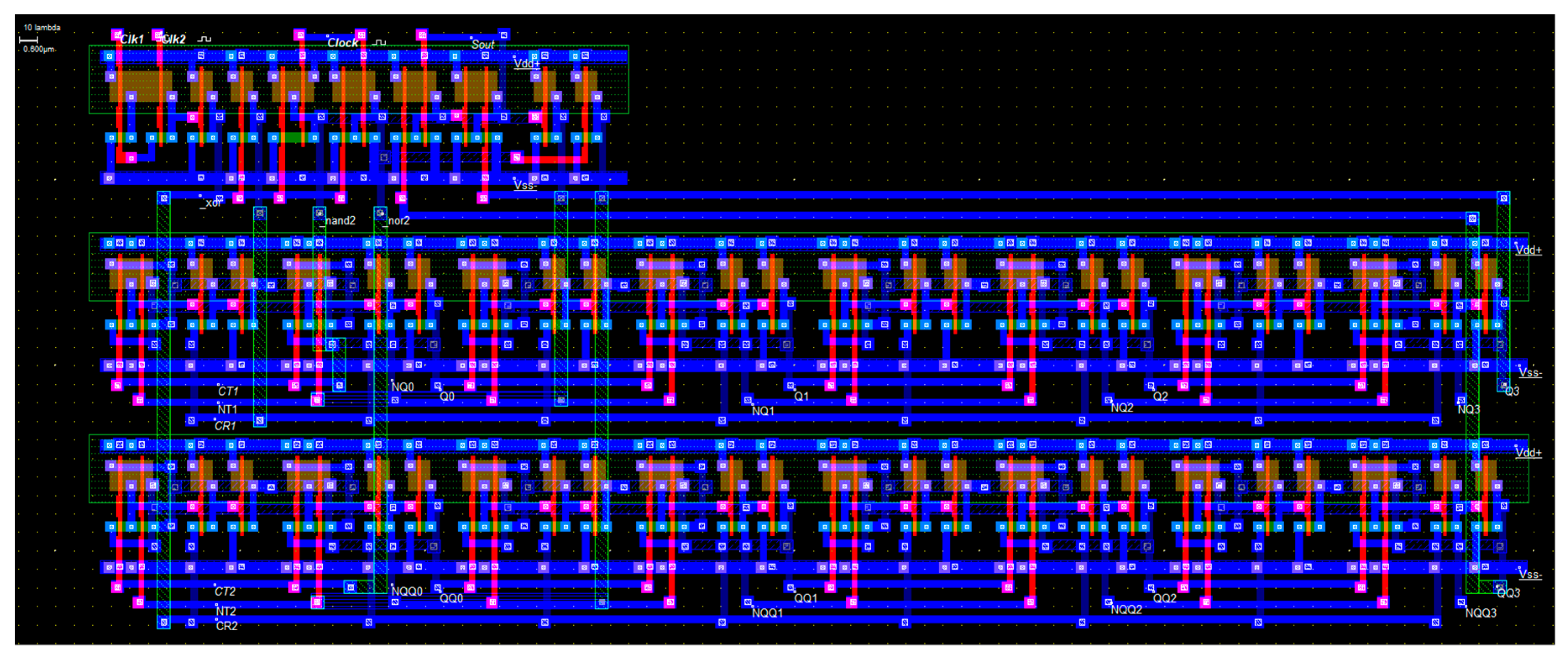
A layout of IC implementation of the fully digital frequency-based SPD scheme for CMOS 0.12 μm technology is presented in Figure 11. The project was implemented in layout editor of CAD Microwind [24].
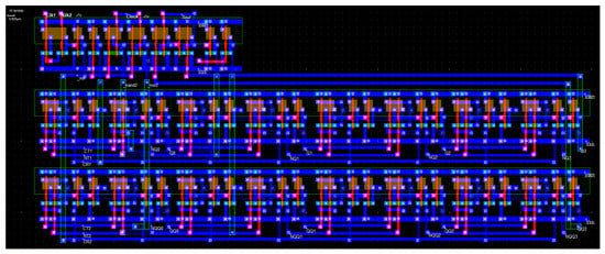
Figure 11.
A layout of fully digital open-loop frequency-based SPD for CMOS 0.12 μm technology.
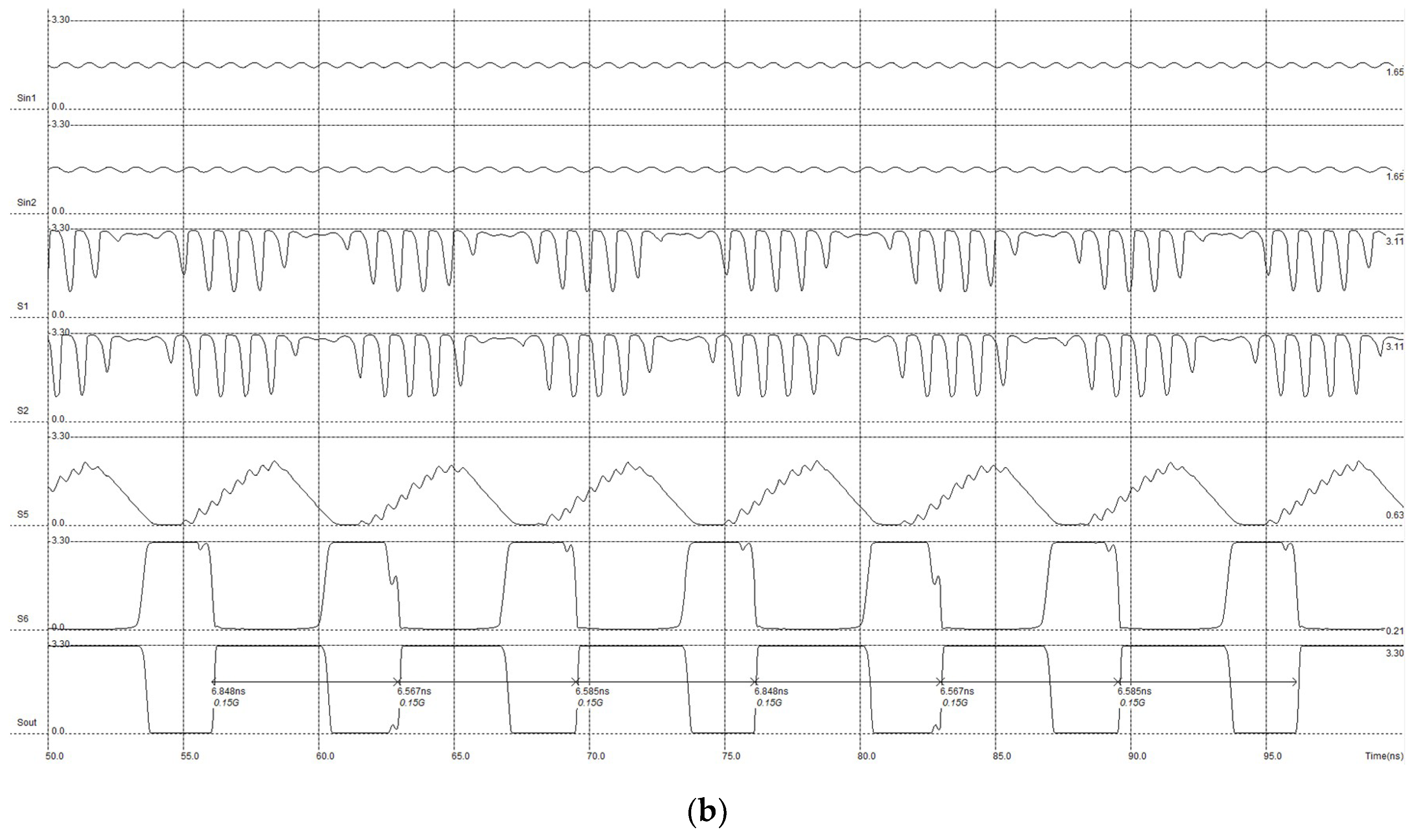
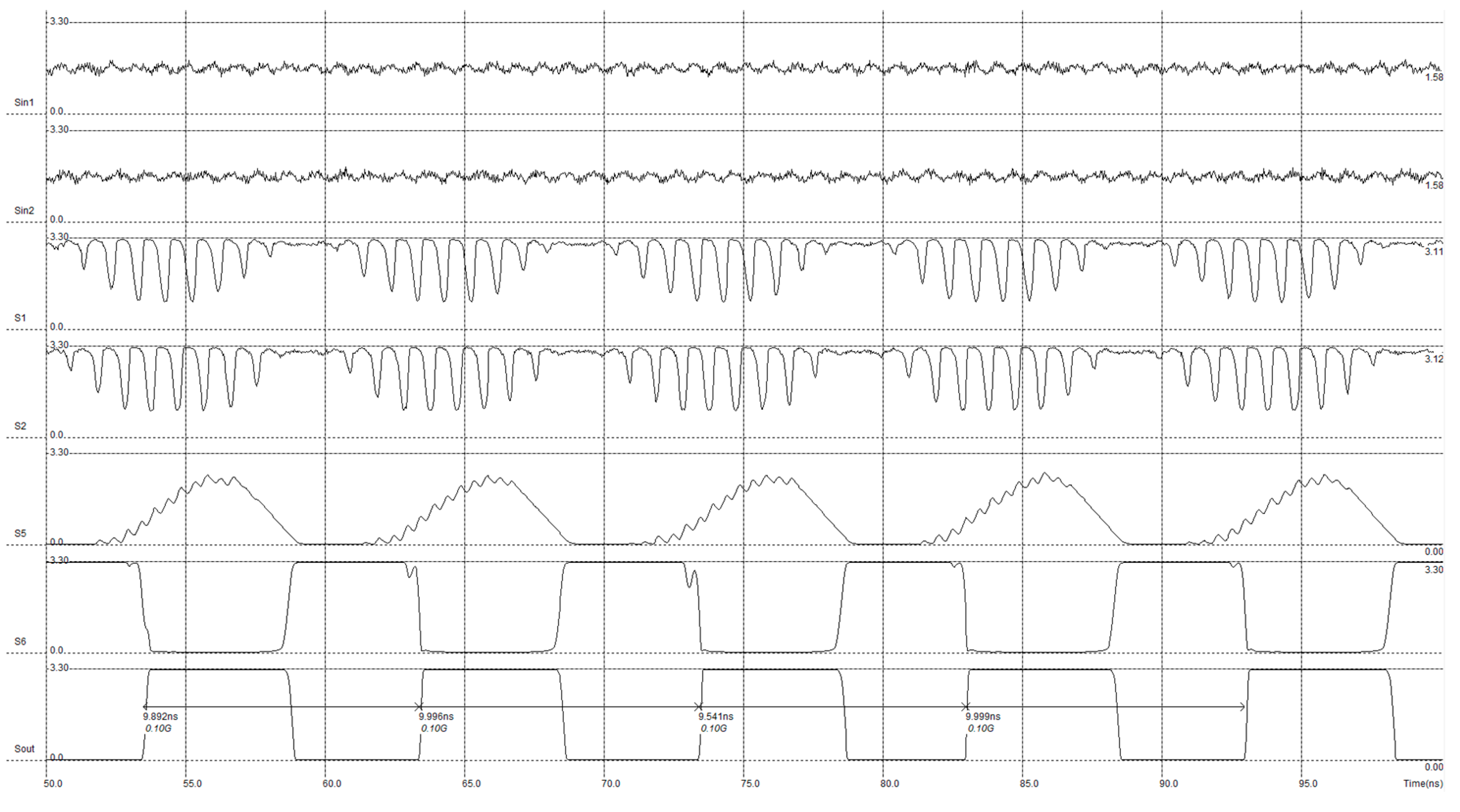
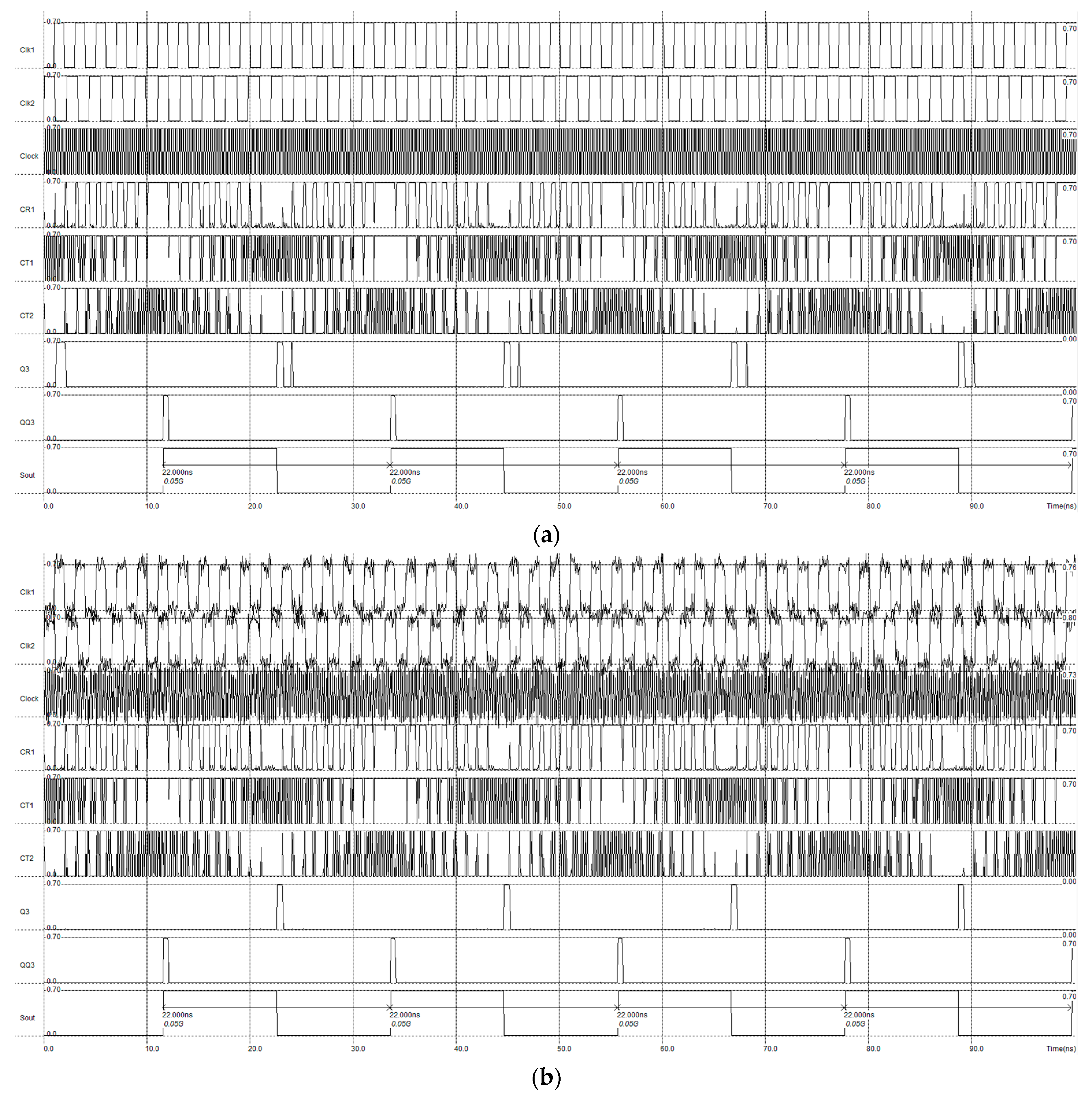
Results of electrical modeling of the digital frequency-based SPD project for the period of output pulses TD = 36 ns (differential frequency fD = 27.78 MHz) are shown in Figure 12.

Figure 12.
Transients of digital frequency-based SPD project (CMOS 0.12 μm technology) and for TD = 36 ns, fD = 27.78 MHz.
Basic parameters of CMOS 0.12 μm technology for digital frequency-based SPD are presented in Table 5.
Table 5.
Basic parameters of CMOS 0.12 μm technology for digital frequency-based SPD.
According to the scheme of the considered SPD in Figure 10 and transients in Figure 12, rectangular digital signals Clk1 and Clk2 of the oscillators were fed to the inputs of the mixer (XOR element DD1), which formed the signal CR1. Frequency of the signal Clk2 was dependent on the measured acceleration f1 ± Δf(ax). The frequency of the signal Clk1 was independent of the acceleration. Pulse duration of CR1 was modulated by phase difference of input signals Clk1 and Clk2.
Next, the signal CR1 was fed to the inputs of two functional blocks for determining the duration of the output pulses of the mixer and the intervals between these pulses. The block for determining the duration of the mixer pulses included the elements AND (DD3), NOT (DD4), and counter DD6. Correspondently, the block for determining the intervals between mixer pulses included the element OR (DD2) and counter DD5. Element DD3 filled the pulses of the CR1 with pulses of the clock-generator (signal Clock). Correspondently, element DD2 was filled by pulses of the signal clock at the intervals between pulses of the CR1 (Figure 12). Output signal CT1 of the OR element DD2 was fed to the counting input C of the counter DD5. Output signal CT2 of the AND element DD3 was fed to the counting input C of the counter DD6. On the reset-inputs R of the counters DD5 and DD6 a direct (on the R input of DD5) and an inversed by inverter DD4 (on the R input of DD6) mixer’s signal CR1 were fed.
The outputs Q of counters DD5 (signal Q3) and DD6 (signal QQ3) were the high bits of the output buses of the counters. A high logic level on these outputs was formed when maximum pulse duration of CR1 (for QQ3) or maximum interval between pulses of CR1 (for Q3) occurred (Figure 12). For this purpose, the following ratio between frequency f0 of Clk1 and Clock-frequency fClock is necessary:
where B is a number of bits of the counter’s output bus.
2B−1 ⋅ f0 ≤ fClock < 2B ⋅ f0,
Next, the counter output signals Q3 and QQ3 were fed to the inputs of the RS-trigger on the NOR elements DD7 and DD8. The RS-trigger formed an output signal Sout with differential-frequency fD (Figure 12).
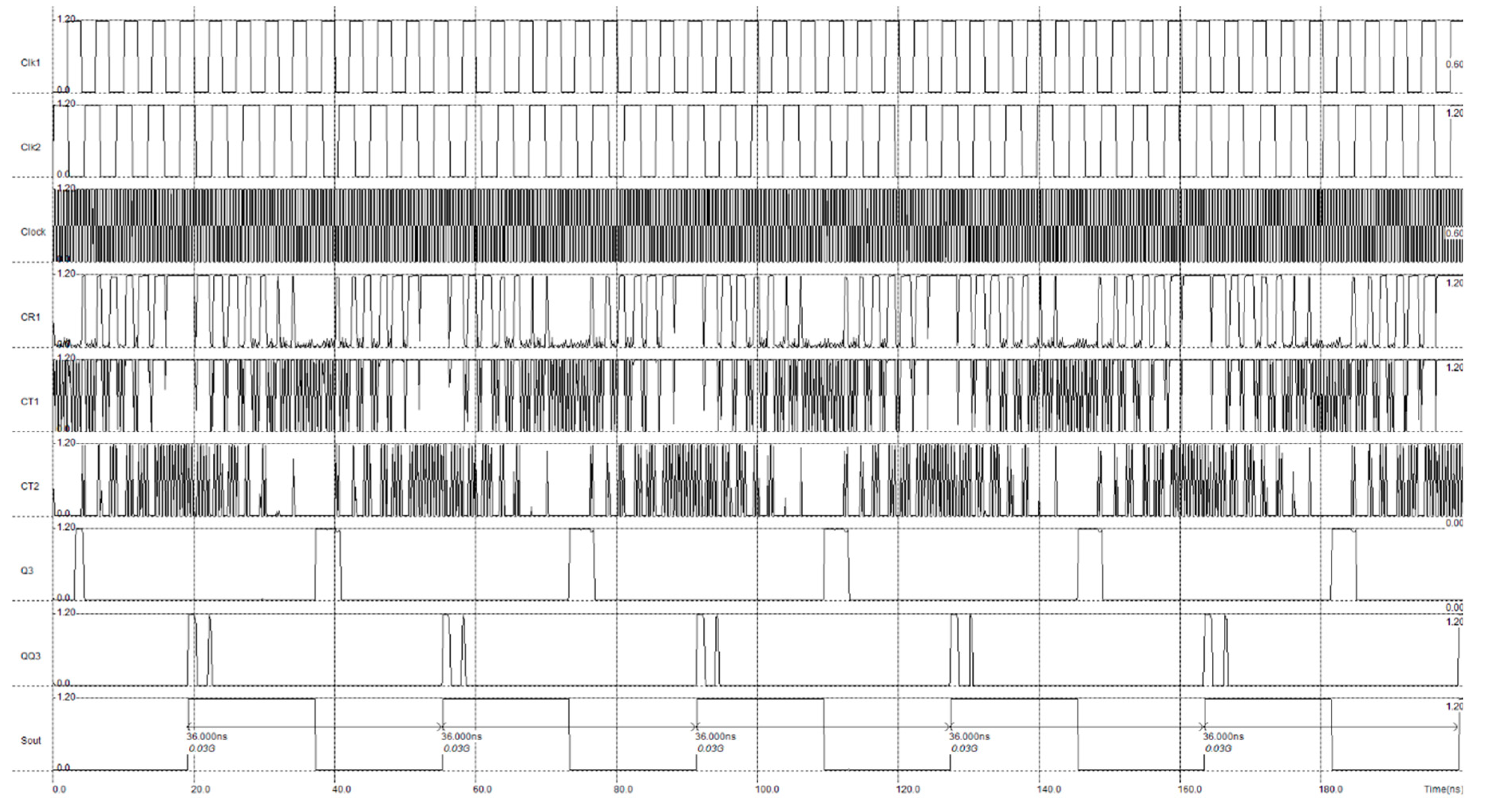
In the considered digital SPD layout presented in Figure 10, the number of bits of the counter’s output bus (B) was equal to four. According to Equation (20) and taking into account the parameters of CMOS 0.12 μm technology, following frequencies for transients in Figure 12 were selected: fClock = 2.5 GHz and f0 = 250 MHz.
The frequency f0 of digital SPD was lower than in the analog SPD project considered in Section 3 due to Equation (20). Therefore, in accordance with Equations (11) and (13), the sensitivity and a dynamic range of the digital SPD were lower too. In contrast to the analog SPD project, the digital SPD project is fully scalable for various CMOS technologies. For example, and to illustrate the noise immunity of the considered SPD, Figure 13 shows the transients of the digital SPD project in the same manner as the Figure 10 layout for the CMOS 50 nm technology, of which basic parameters are presented in Table 6. The transients in Figure 13 were modeled for fClock = 5 GHz, f0 = 500 MHz and for input signals Clk1, Clk2 and Clock with an RMS noise NRMS = 0.5 V (Figure 13b).
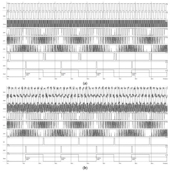
Figure 13.
Transients of the digital frequency-based SPD project (CMOS 50 nm technology) for fClock = 5 GHz, f0 = 500 MHz, TD = 22 ns and fD = 45.45 MHz: without noise of input signals (a) and with noise of input signals for RMS noise NRMS = 0.5 V (b).
Table 6.
Basic parameters of CMOS 50 nm technology for digital frequency-based SPD.
As the transients in Figure 12 and Figure 13 show, the functionality of the digital frequency-based SPD was independent of the CMOS technology parameters. Comparative analysis of the ideal and noised transients in Figure 13a,b shows that even for comparatively high RMS noise of input signals Clk1, Clk2 and Clock (NRMS = 0.5 V) the jitter of the output signal Sout was not increased in contrast to the analog SPD project transients considered in Section 3. This is because the noise of the input signals can change mainly the shape of the output signal, while the informative parameter of the output signal is its frequency.
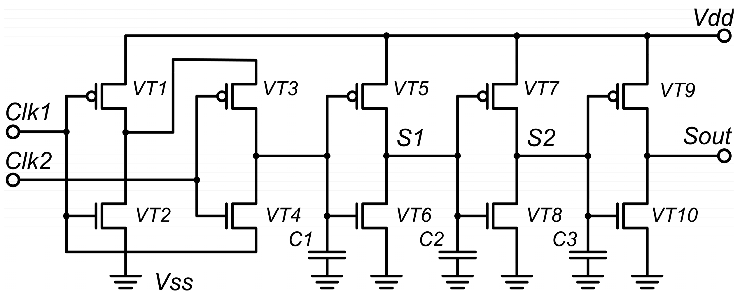
5. Mixed-Signal Scheme of SPD Project
The third open-loop frequency-based SPD IP-core project was a mixed-signal project. A scheme of this SPD without oscillators is presented in Figure 14. This project combined the advantages of the analog and fully digital SPDs considered in Section 3 and Section 4. Like the fully digital SPD, this mixed-signal project uses LC oscillators of digital rectangular pulses (input signals Clk1 and Clk2 in Figure 14) and a mixer on the bases of XOR CMOS-element on the transistors VT1–6. In contrast to the digital SPD, in this case, like the analog SPD project, the synthesis of the output rectangular differential-frequency signal Sout used two series-connected CMOS-inverters on the transistors VT7–10 and low-pass filters based on the capacitors C1, C2 and C3. The first low-pass filter C1 was included in the XOR scheme in accordance with Figure 14.

Figure 14.
Mixed-signal CMOS-scheme of open-loop frequency-based SPD project.
A layout of IC implementation of the mixed-signal frequency-based SPD scheme for CMOS 50 nm technology, of which basic parameters are presented in Table 6, is shown in Figure 15. The project was implemented in layout editor of CAD Microwind [24].
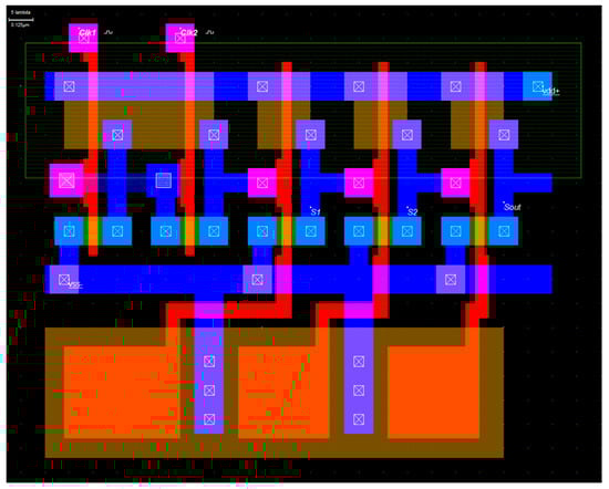
Figure 15.
A layout of a mixed-signal open-loop frequency-based SPD for CMOS 50 nm technology.
The parameters of the capacitors C1–3 are presented in Table 7.
Table 7.
Parameters of the capacitors C1–3 of mixed-signal frequency-based SPD.
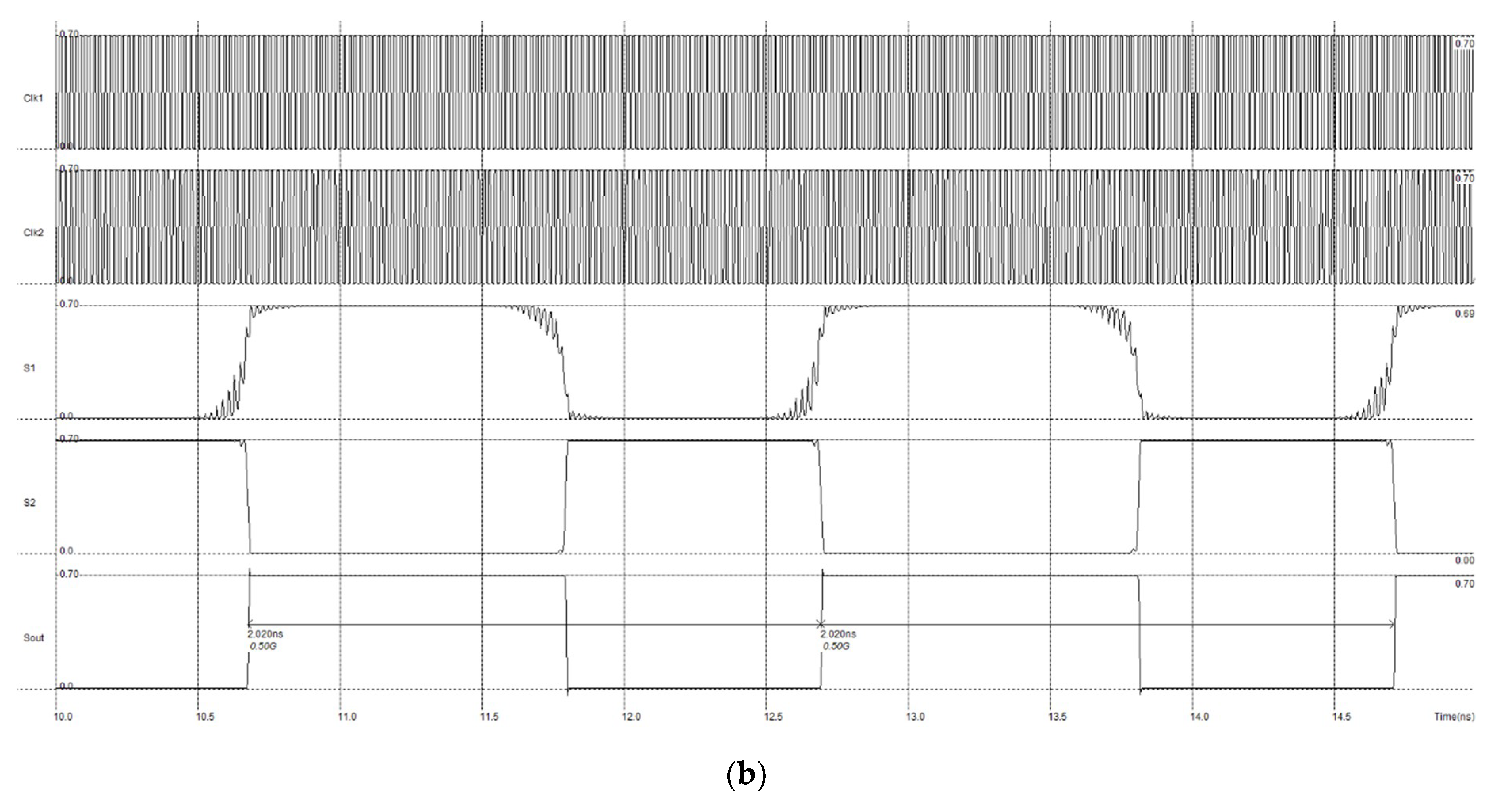
Results of electrical modeling of the mixed-signal frequency-based SPD project for a frequency of the signal Clk1 are as follows: f0 = 50 GHz, initial frequency of the signal Clk2 f1 = 48.08 GHz, period of output pulses TD = 520 ps, initial differential frequency fD0 = 1.92 GHz are shown in (Figure 16).
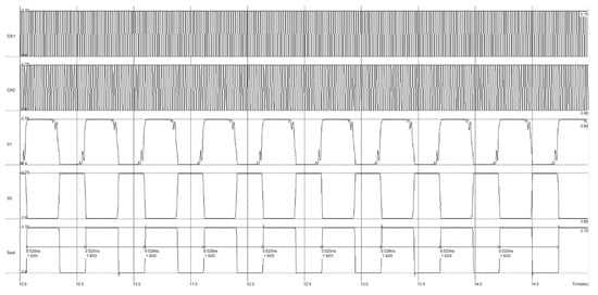
Figure 16.
Transients of the mixed-signal frequency-based SPD project (CMOS 50 nm technology) for initial conditions Δf = 0, f0 = 50 GHz, TD = 520 ps and fD0 = 1.92 GHz.
According to the scheme in Figure 14 and transients in Figure 16, rectangular digital signals Clk1 and Clk2 of the oscillators were fed to the inputs of a XOR-mixer (VT1–6) with low-pass filter (C1), which formed a signal S1 with differential frequency fD. Frequency of the signal Clk2 was dependent on the measured acceleration f1 ± Δf(ax). Frequency f0 of the signal Clk1 was independent of the acceleration. Next, two series-connected inverters on transistors VT7–10 and low-pass filters on capacitors C2 and C3 deleted pulsations of the signal S1 and formed the output digital signal Sout.
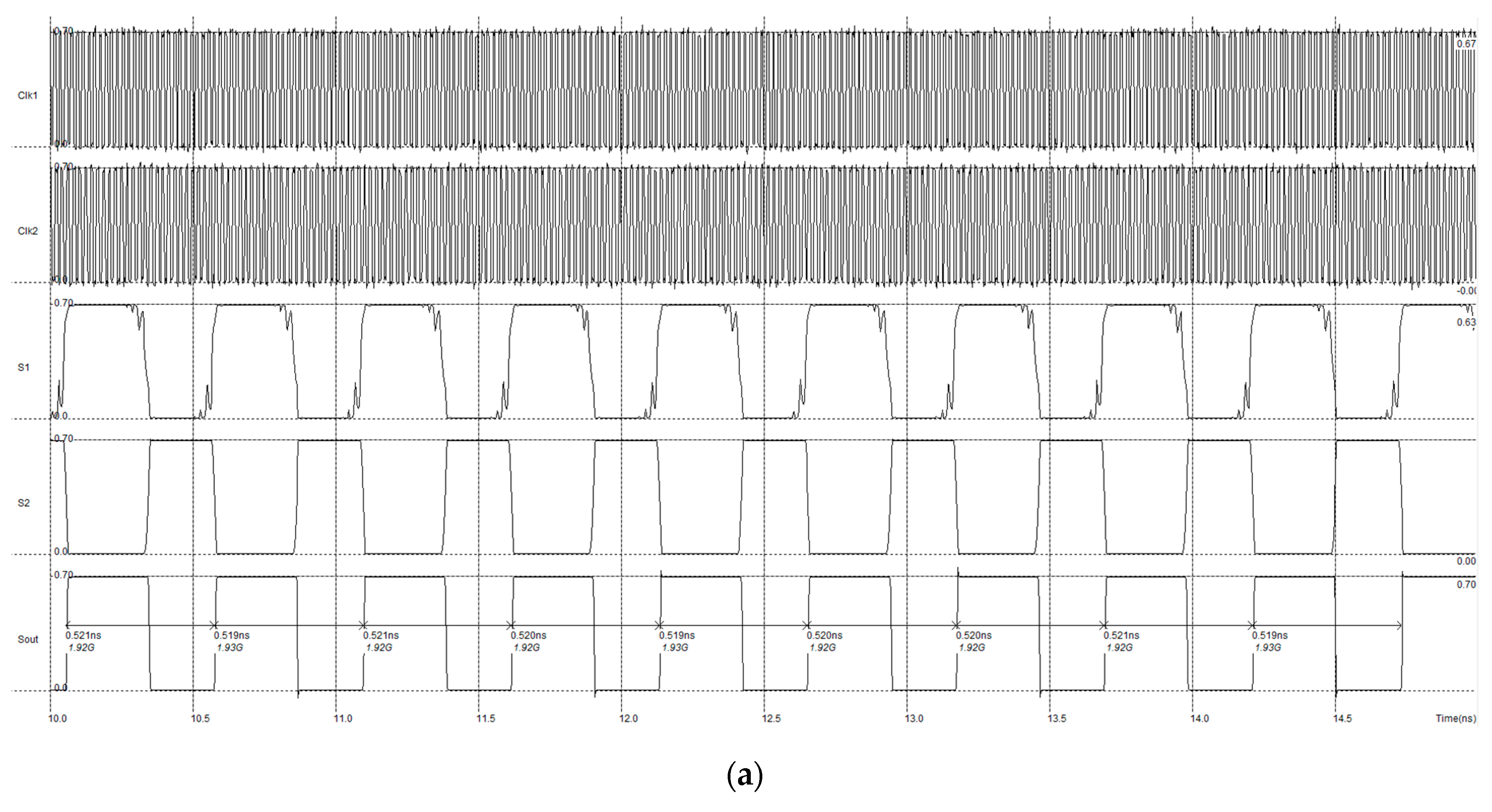
Figure 17 presents the transients for positive (Δf = 0.46 GHz and fD = 2.38 GHz, Figure 17a) and negative (Δf = −1.42 GHz and fD = 0.5 GHz, Figure 17b) directions of measured acceleration.
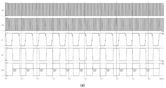
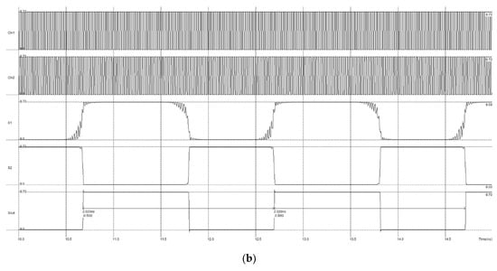
Figure 17.
Transients of the mixed-signal frequency-based SPD project (CMOS 50 nm technology) for positive (Δf = 0.46 GHz and fD = 2.38 GHz (a)) and negative (Δf = −1.42 GHz and fD = 0.5 GHz (b)) directions of measured acceleration.
To study a noise immunity of the mixed-signal frequency-based SPD, an analysis of the transients for noised input signals Clk1 and Clk2 with a band of RMS noise 0.1–0.7 V was executed. Figure 18 shows the noised transients for initial conditions (Δf = 0, f0 = 50 GHz and fD0 = 1.92 GHz) with RMS noise NRMS = 0.1 V (Figure 18a) and NRMS = 0.5 V (Figure 18b). Figure 19 presents the dependence of an output signal jitter on RMS noise of the input signals. This dependence was obtained by statistical averaging over a sample of 25 transients for each RMS noise value.
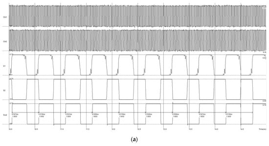
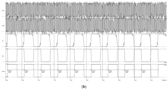
Figure 18.
Transients of the mixed-signal frequency-based SPD project (CMOS 50 nm technology) with noised input signals for initial conditions Δf = 0, f0 = 50 GHz and fD0 = 1.92 GHz with noise RMS NRMS = 0.1 V (a) and NRMS = 0.5 V (b).
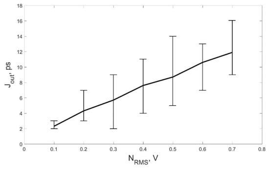
Figure 19.
Dependence of output signal jitter on RMS noise of the input signals for mixed-signal SPD.
In accordance with the dependence in Figure 19, jitter Jout of output differential-frequency signal Sout monotonously increased with increasing RMS of input noise. Even for high RMS of input noise 0.1–0.7 V, the output jitter Jout was less than 2–16 ps, which corresponds to 0.4–3% of the period of output signal. Moreover, as it was shown in Section 2.4, output frequency measuring during post-processing significantly decreased the influence of output jitter on the post-processing results due to averaging of the output signal period TD on the period of high-stability clock oscillator TCLK.
6. Results of Comparative Analysis and Discussion
Comparative analysis of three developed IP-core projects of highly sensitive open-loop signal processing devices with frequency output for capacitive MEMS accelerometers allows the following conclusions to be made.
The analog project of frequency-based SPD considered in Section 3 has a comparatively simple CMOS scheme (12 transistors and three capacitors in Figure 4). It uses high-frequency harmonic oscillators, the frequencies of which are limited only by the parameters of the CMOS-technology used and power dissipation requirements. In accordance with Equations (11) and (13), high frequency of the oscillators increases sensitivity and expands dynamic range of MEMS-accelerometers with the considered SPD. According to Figure 9, functionality of this frequency-based SPD is saved even for RMS noise of input signals (NRMS = 0.5 V) higher than amplitude of these signals (0.1 V). However, noise of input signals increases a jitter of output signal Sout to 0.41 ns, which is 4.1% of the period of Sout.
Compatibility with CMOS-technologies is an important feature of all three SPD projects considered in this study. The drawback of the analog SPD project is a bad scalability. When the CMOS-technology used is changed, a full range of project calculations and modeling is needed to provide a good functionality and necessary values of the parameters.
The fully digital project of frequency-based SPD considered in Section 4 has a more complex CMOS scheme (Figure 10) than the analog one. In contrast to the analog SPD scheme, oscillators of digital rectangular pulses are used. The frequency of sensing oscillators in digital SPD is considerably lower than in the analog one due to the necessity of a clock-generator, the frequency of which is connected with the frequency of sensing oscillators by Equation (20). Therefore, in accordance with Equations (11) and (13), the sensitivity and dynamic range of digital SPD are lower too. In contrast to the analog SPD project, the digital SPD project is fully scalable for various CMOS technologies. This is confirmed by transients of digital SPD projects for both 120 nm (Figure 12) and 50 nm (Figure 13) CMOS-technologies.
The mixed-signal project of frequency-based SPD considered in Section 5 combines the advantages of the analog and fully digital SPD considered in Section 3 and Section 4. Like the digital SPD, this mixed-signal project uses oscillators of digital rectangular pulses and a mixer on the bases of XOR CMOS-element. In contrast to the digital SPD and like to the analog SPD project, two series-connected CMOS-inverters and low-pass filters are used to synthesize the output rectangular differential-frequency signal. This approach the scheme of SPD to be simplified, excluding a clock-generator, increasing the frequency of the oscillators to maximum values (which are determined by the CMOS-technology and by permissible level of a phase noise), increasing sensitivity and widening dynamic range. It should be noted, that like the digital SPD, the mixed-signal project is well scalable for various CMOS technologies.
In accordance to the dependence in Figure 19, jitter of output SPD signal is monotonously increased with an increasing RMS of input noise. But even for high RMS of input noise 0.1–0.7 V, the output jitter in mixed-signal SPD is less than 0.4–3% of the period of output signal. Moreover, as it was shown in Section 2.4, the influence of the considered output jitter on the accuracy of acceleration measuring will be significantly decreased due to averaging of the output signal period during post-processing.
Results of comparative analysis of the proposed frequency-based SPD projects are briefly presented in Table 8.
Table 8.
Properties of developed frequency-based signal processing devices.
7. Conclusions
This paper focuses on open-loop frequency-based signal processing devices (SPD) for capacitive MEMS accelerometers. The considered frequency-based readout circuits have some advantages to compare with widely used voltage-based SPD, such as a high sensitivity, noise immunity, wide dynamic range and resistance to temperature changes.
In this paper, the differential frequency principle of the open-loop frequency-based SPD is used to develop three CMOS IP-core projects of highly sensitive readout circuits with frequency output: analog, digital and mixed-signal. These signal processing devices form the output rectangular pulses, the frequency of which equals a difference of signal frequencies of two oscillators, one of which contains a micromechanical accelerometer capacitive transducer in the frequency control circuit.
According to the results of the comparative analysis, the analog circuit of the project is characterized by high sensitivity and dynamic range due to the high frequency of oscillators. At the same time, the layout of the analog SPD project is not scalable for various CMOS technologies.
In contrast to this, the digital project is fully scalable for various CMOS-technologies due to the digital rectangular pulses of oscillators and digital mixer. However, the frequency of sensing oscillators in digital SPD is considerably lower than in the analog one due to the necessity of a clock-generator. Correspondently, sensitivity and dynamic range of digital SPD are lower too.
The mixed-signal project combines the advantages of the analog and digital projects. Therefore, the mixed-signal project is a most promising candidate to comprehensively increase the basic parameters of considered frequency-based signal processing devices.
According to the results of modeling, all considered SPD projects demonstrate a high immunity to noise fluctuations of input voltages because not voltage, but frequency is an informative parameter of readout circuit’s output signal and due to the lack of high-gain operational amplifiers. Even for high RMS of input noise 0.1–0.7 V, the output jitter in mixed-signal SPD is less than 0.4–3% of the period of the output signal. Accordingly, only the phase noise of the LC oscillators is the main contribution to the jitter of the output signal, which can be significantly reduced during the post-processing.
It is important to note, that open-loop frequency-based signal processing devices proposed in this study can be successfully used for various capacitive sensors, such as accelerometers, gyroscopes, pressure sensors, inclinometers, etc.
8. Patents
RU 2602493 C1, 20.11.2016.
Author Contributions
Conceptualization, E.R. and B.K.; Formal analysis, E.R. and B.K.; Investigation, E.R., B.K., I.L., I.K. and A.P.; Writing—original draft, E.R.; Writing—review & editing, E.R. and B.K.
Funding
This research was funded by Southern Federal University of Russia.
Conflicts of Interest
The authors declare no conflict of interest.
References
- Zhu, B.; Han, J.; Zhao, J. Tire-Pressure Identification Using Intelligent Tire with Three-Axis Accelerometer. Sensors 2019, 19, 2560. [Google Scholar] [CrossRef] [PubMed]
- Shevchenko, S.Y.; Khivrich, M.A.; Markelov, O.A. Ring-Shaped Sensitive Element Design for Acceleration Measurements: Overcoming the Limitations of Angular-Shaped Sensors. Electronics 2019, 8, 141. [Google Scholar] [CrossRef]
- Straczkiewicz, M.; Glynn, N.W.; Harezlak, J. On Placement, Location and Orientation of Wrist-Worn Tri-Axial Accelerometers during Free-Living Measurements. Sensors 2019, 19, 2095. [Google Scholar] [CrossRef] [PubMed]
- Trinh, H.X.; Iwamoto, Y.; Ho, V.A.; Shibuya, K. Localization of Sliding Movements Using Soft Tactile Sensing Systems with Three-axis Accelerometers. Sensors 2019, 19, 2036. [Google Scholar] [CrossRef] [PubMed]
- Shen, Q.; Yang, D.; Zhou, J.; Wu, Y.; Zhang, Y.; Yuan, W. A Measurement-Data-Driven Control Approach towards Variance Reduction of Micromachined Resonant Accelerometer under Multi Unknown Disturbances. Micromachines 2019, 10, 294. [Google Scholar] [CrossRef]
- Yazdi, N.; Farrokh, A.; Khalil, N. Micromachined inertial sensors. Proc. IEEE 1998, 86, 1640–1659. [Google Scholar] [CrossRef]
- Rao, K.; Wei, X.; Zhang, S.; Zhang, M.; Hu, C.; Liu, H.; Tu, L.-C. A MEMS Micro-g Capacitive Accelerometer Based on Through-Silicon-Wafer-Etching Process. Micromachines 2019, 10, 380. [Google Scholar] [CrossRef]
- Li, X.; Hu, J.; Liu, X. A High-Performance Digital Interface Circuit for a High-Q Micro-Electromechanical System Accelerometer. Micromachines 2018, 9, 675. [Google Scholar] [CrossRef]
- Yan, S.; Xie, Y.; Zhang, M.; Deng, Z.; Tu, L. A Subnano-g Electrostatic Force-Rebalanced Flexure Accelerometer for Gravity Gradient Instruments. Sensors 2017, 17, 2669. [Google Scholar] [CrossRef]
- Baxter, L.K. Capacitive Sensors: Design and Applications; IEEE Press: Piscataway, NJ, USA, 1997; pp. 1–17. [Google Scholar]
- Kim, M.; Moon, W.; Yoon, E.; Lee, K.-R. A new capacitive displacement sensor with high accuracy and long-range. Sens. Actuators A Phys. 2006, 130–131, 135–141. [Google Scholar] [CrossRef]
- Li, S.; Gao, Y.; Meng, G.; Wang, G.; Guan, L. Accelerometer-Based Gyroscope Drift Compensation Approach in a Dual-Axial Stabilization Platform. Electronics 2019, 8, 594. [Google Scholar] [CrossRef]
- Wu, W.; Zheng, P.; Liu, J.; Li, Z.; Fan, J.; Liu, H.; Tu, L. High-Sensitivity Encoder-Like Micro Area-Changed Capacitive Transducer for a Nano-g Micro Accelerometer. Sensors 2017, 17, 2158. [Google Scholar] [CrossRef] [PubMed]
- Wang, C.; Tsai, M.-H.; Sun, C.-M.; Fang, W. A novel CMOS out-of-plane accelerometer with fully differential gap-closing capacitance sensing electrodes. J. Micromech. Microeng. 2007, 17, 1275–1280. [Google Scholar] [CrossRef]
- Chen, D.; Liu, X.; Yin, L.; Wang, Y.; Shi, Z.; Zhang, G. A Σ∆ Closed-Loop Interface for a MEMS Accelerometer with Digital Built-In Self-Test Function. Micromachines 2018, 9, 444. [Google Scholar] [CrossRef]
- Fleming, A.J. A review of nanometer resolution position sensors: Operation and performance. Sens. Actuators A Phys. 2013, 190, 106–126. [Google Scholar] [CrossRef]
- Lv, R.; Fu, Q.; Yin, L.; Gao, Y.; Bai, W.; Zhang, W.; Zhang, Y.; Chen, W.; Liu, X. An Interface ASIC for MEMS Vibratory Gyroscopes with Nonlinear Driving Control. Micromachines 2019, 10, 270. [Google Scholar] [CrossRef] [PubMed]
- Liu, H.; Fang, R.; Miao, M.; Zhang, Y.; Yan, Y.; Tang, X.; Lu, H.; Jin, Y. Design, Fabrication, and Performance Characterization of LTCC-Based Capacitive Accelerometers. Micromachines 2018, 9, 120. [Google Scholar] [CrossRef]
- Qiao, Z.; Boom, B.A.; Annema, A.-J.; Wiegerink, R.J.; Nauta, B. On Frequency-Based Interface Circuits for Capacitive MEMS Accelerometers. Micromachines 2018, 9, 488. [Google Scholar] [CrossRef]
- Enz, C.C.; Temes, G.C. Circuit techniques for reducing the effects of op-amp imperfections: Autozeroing, correlated double sampling, and chopper stabilization. Proc. IEEE 1996, 84, 1584–1614. [Google Scholar] [CrossRef]
- Razavi, B. A Study of Injection Locking and Pulling in Oscillators. IEEE J. Solid-State Circuits 2004, 39, 1415–1424. [Google Scholar] [CrossRef]
- Mirzaei, A.; Darabi, H. Mutual Pulling Between Two Oscillators. IEEE J. Solid-State Circuits 2014, 49, 360–372. [Google Scholar] [CrossRef]
- Wang, H.; Weng, C.C.; Hajimiri, A. Phase Noise and Fundamental Sensitivity of Oscillator-Based Reactance Sensors. IEEE Trans. Microw. Theory Tech. 2013, 61, 2215–2229. [Google Scholar] [CrossRef]
- Sicard, E. Microwind & Dsch. Version 3.5. User’s Manual; INSA, University of Toulouse: Toulouse, France, 2009; pp. 1–130. [Google Scholar]


© 2019 by the authors. Licensee MDPI, Basel, Switzerland. This article is an open access article distributed under the terms and conditions of the Creative Commons Attribution (CC BY) license (http://creativecommons.org/licenses/by/4.0/).