Article

Design of an Intrinsically Safe Series-Series Compensation WPT System for Automotive LiDAR

1
Centro ALGORITMI; University of Minho, 4800-058 Guimarães, Portugal
2
Bosch Car Multimedia Portugal, S.A. Rua do Barrio de Cima, n°1, 4705-820 Braga, Portugal
3
CMEMS-UMinho Center, University of Minho, 4800-058 Guimarães, Portugal
*
Author to whom correspondence should be addressed.
Electronics 2020, 9(1), 86; https://doi.org/10.3390/electronics9010086
Submission received: 30 November 2019 / Revised: 17 December 2019 / Accepted: 27 December 2019 / Published: 1 January 2020
(This article belongs to the Section Power Electronics)

Abstract

:
The earliest and simplest impedance compensation technique used in inductive wireless power transfer (WPT) design is the series-series (SS) compensation circuit, which uses capacitors in series with both primary and secondary coils of an air-gapped transformer. Despite of its simplicity at the resonant condition, this configuration exhibits a major sensitivity to variations of the load attached to the secondary, especially when higher coupling coefficients are used in the design. In the extreme situation that the secondary coil is left at open circuit, the current at the primary coil may increase above the safety limits for either the power converter driving the primary coil or the components in the primary circuit, including the coil itself. An approach often used to minimize this problem is detuning, but this also reduces the electrical efficiency of the power transfer. In low power, fixed-distance stationary WPT, a fair trade-off between efficiency and safety must be verified. This paper aims to consolidate a simple design procedure for such a SS-compensation, exemplifying its use in the prototype of a WPT system for automotive light detection and ranging (LiDAR) equipment. The guidelines herein provided should equally apply to other low power applications.

1. Introduction

The possibility of energizing different apparatuses by inductive wireless power transfer (WPT) is very appealing, and the technology becomes more popular as it is continually improved to achieve higher electrical efficiency and power levels, with the use of modern components and simple circuitry design techniques, what results in low cost of implementation. WPT exploits the near field properties of electromagnetism, as consolidated by James C. Maxwell, in his 1873 treatise [1]. In a sequence of experiments from 1886 to 1889 [2], while seeking evidence for the electromagnetic waves predicted by Maxwell, Heinrich R. Hertz first came across WPT, realizing that it was possible to produce a spark in between the terminals of a Riess coil, when switching electric current in another of these coils, positioned close to the first one, in a parallel plane [3]. This short range phenomenon, that can be purely credited to magnetic induction, constituted a wireless extension of the “cored” induction, discovered by Faraday in 1831, in his ring transformer experiment [4,5], which, among other observations, had provided Maxwell the experimental evidence for his treatise itself.
While the “cored” type induction soon found industrial use in electric transformers [6], near field, coreless WPT remained mostly restricted to laboratory demonstrations, due to technological limitations of that time for generating large electric currents at high frequencies. Nikola Tesla, in the late 19th century, successfully developed WPT-based apparatuses and did several public demonstrations. However, Tesla mostly used inductive WPT for exciting large secondary coils and generating high electric voltages and oscillating electrostatic fields, in lightening experiments, in such a way that the dominating power transfer mechanism in these experiments was capacitive [7]. Seeking wireless power transmission, later on he apparently concentrated in the development of far field technology (radio waves), which eventually gained public attention much faster in communications applications, rather than power transfer applications [8]. Only more recently, inductive WPT was rediscovered by researchers [9,10] and reintroduced in consumer applications. It may have limitations associated with high implementation costs, low efficiency, sensitiveness to misalignments, short transfer range, and safety issues, if not carefully designed. However, in some applications, the use of WPT is extremely convenient, due to the mechanical constraints involved. This is the case of the design of an automotive light detection and ranging (LiDAR) for autonomous navigation, where the LiDAR optics and primary video signal processing is located in a revolving head that continuously scans the environment.
This paper tries to consolidate some guidelines for designing and checking a WPT configuration using SS-compensation, highlighting some of the procedures and best practices either reported or implicit in recent work. However, instead of optimizing the maximum power or power efficiency, as in most theoretical investigations found in literature, another convenient design directive is to assure intrinsic safe operation under load disconnection, while maintaining the required transferred power at reasonable efficiency under nominal load conditions. This trade-off is especially acceptable in low power applications where safety, stability, circuit simplicity and cost effectiveness can be more important than optimality in electrical efficiency.
The application that motivated this work, is the integration of high rate wireless data transfer and wireless powering of a LiDAR equipment in an automotive environment, where the gap distance is fixed, and the WPT frequency can be constant. In this sense, Section 2 presents a brief description of the LiDAR characteristics, and explains the relevance of using WPT for energizing this type of equipment. In Section 3, a WPT model and design guidelines are provided, including design steps such as the selection of a magnetic coupling pair, the operation frequency, and the primary and secondary circuitries. In Section 4, the WPT design procedure using series-series (SS)-compensation is exemplified, with the partial use of simulation resources to compute and preliminarily validate the design. In Section 5, results from the implemented prototype are provided, which confirm a good balance between efficiency and safety of operation. Finally, a discussion of the results and concluding remarks are presented in Section 6.

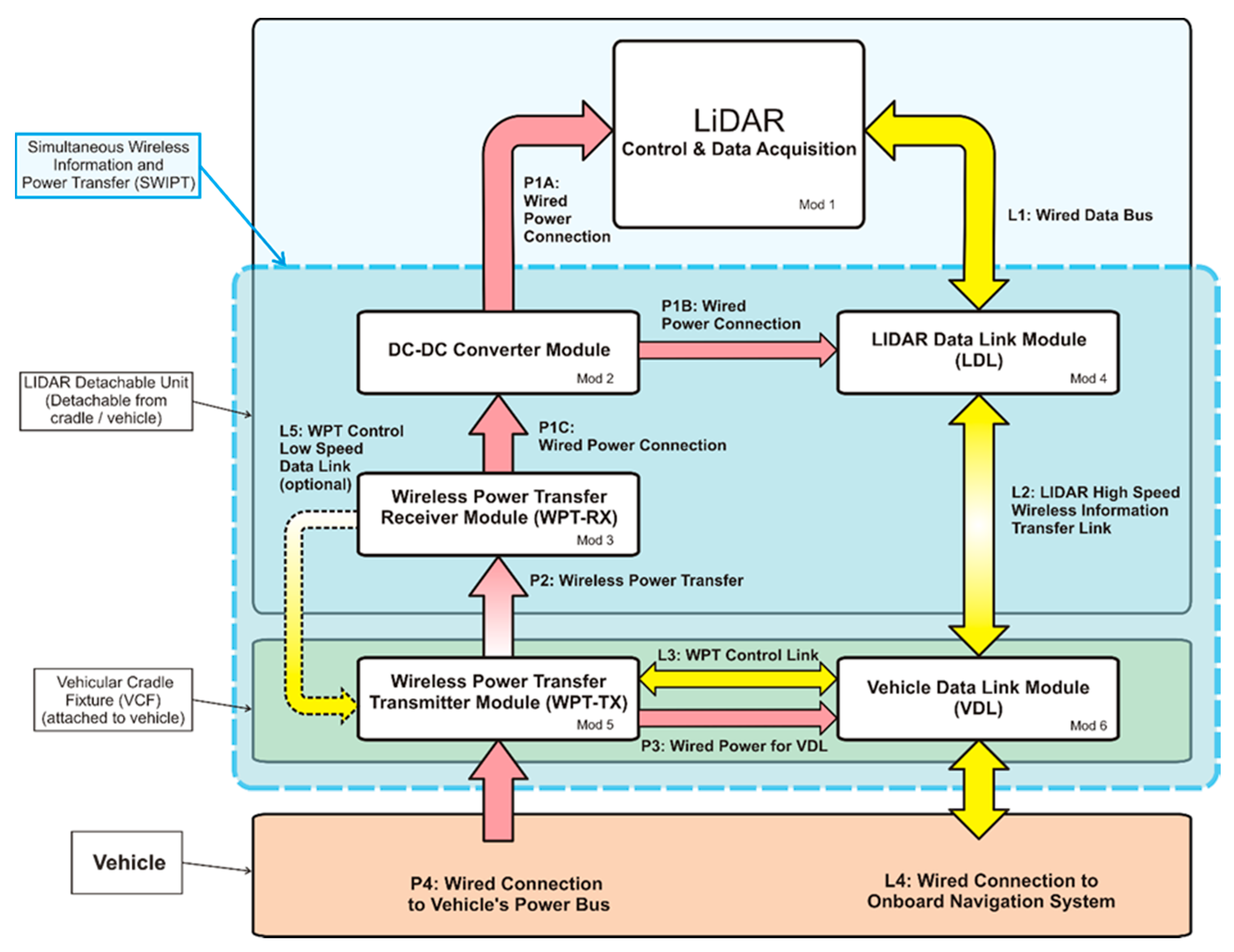
2. LiDAR Requirements for Simultaneous Information and Power Transfer

This section presents a description of the LiDAR technology, including innovative features as the simultaneous wireless information and power transfer, and establishes a motivational bridge to the contributions of this paper. It is also briefly explained the relevance of using WPT for energizing this type of equipment, pointing out the need to accommodate WPT with high rate wireless information transfer and listing initial requirements for such design.

2.1. LiDAR Technology

LiDAR is a technology created in 1960s, consisting of an active system to simultaneously measure the distance and intensity of every point in the scene, by monitoring the time between the emitted and received light pulse, usually called by Time of Flight (ToF), using the same principle as radio detection and ranging (RADAR), developed for target detecting, locating, ranging, and profiling applications. This environment sensor has the potential to supplement current automotive surround sensing systems in the long run, enabling a direct and reliable object detection and a consistent distance-to-object measurement, in safety-critical functions. In order to better understand how LiDAR technology works, it is important to go into more detail on the laser range finding, where a basic diagram is shown in Figure 1. The LiDAR system consists of a laser source, typically with wavelength in the near-infrared (NIR) region, capable of transmitting pulsed or continuous light over the required Field-of-View (FoV), a low noise high-speed receiver capable of detecting and processing the reflected light beam and a low power controlling unit. The laser is controlled using specific electronics, among other parameters, its power output, pulse frequency, and duration (in case of a pulsed usage) can be continuously reprogrammed. The laser rangefinder only detects the distance to one point in its line of sight. To overcome this issue and to acquire information over the required two-dimensional FoV, an optical scanning system (e.g., beam steering using rotating mirrors or rotating scanning mechanism) is used to control the horizontal and vertical direction of the transmitted beam, giving the system a tridimensional perspective. Additionally, a complex optical lens system is internally mounted at the transmitter and receiver ends, allowing a notable improvement on the overall sensor performance. This system is responsible for collimating and shaping the output laser beam, filtering the received echo to eliminate external spurious wavelengths, as sunlight, that tends to add noise and degrade the Signal-to-Noise Ratio (SNR) and sensor’s sensitivity [11], and focusing the latter into the photodetector. The fraction of light that returns to the sensor is converted into an electrical signal proportional to the light intensity via the photodetector and the resulting signal is conditioned, i.e., amplified and filtered, to finally be processed and have the desired information extracted. The information gathered in this signal, in conjunction with the known emission angle, is stored in a controlling unit that processes the data to construct the topographic frame. Consecutively, the collected data is represented as a 3D intensity cloud of the vehicle external environment, where each point corresponds to a beam orientation within the FoV. Afterwards, based on the LiDAR image, conclusions about the vehicle’s surroundings can be drawn, as the presence, location and classification of objects (using recognition algorithms). The LiDAR system is enclosed in a housing that is responsible for withstanding exterior temperature variations, protecting the system hardware and optics against water splashes (e.g., rain) and pressurized steam, and providing immunity to vibrations and shock resistance, so that misalignments in the optical system are avoided. This way, the housing must be hermetically sealed to prevent degradation of the internal assembly. To create this, it is necessary to include an optical aperture (glass cover) for light exchange with the exterior. In addition, the data collected must be somehow transferred to the central processing unit of the car to be conjugated with the information provided by other sensors. For this purpose, several protocols are available, e.g., Ethernet, Controller Area Network (CAN), and wireless technologies (advantageous since wired connections are not required, allowing a fully sealed packaging).
LiDAR is a complementary technology that, together with video cameras and radars, can achieve the 4th and 5th level of autonomous driving, according to the Society of Automobile Engineers (SAE) organization. However, it is also a high precision and complex system, involving many different disciplines. The need for high quality and precision in the majority of the components and the complexity of the system itself, is one of the reasons why LiDARs are so expensive. LiDAR can be a part of an adaptive cruise control system, which monitors the distance or time-gap to the previous and next vehicles, creates an image of the local surrounding (vehicles, pedestrians, and stationary objects like guard rails) and integrates the Car2Car communication, providing, at least, position data, which can be determined by a Global Navigation Satellite System (GNSS), for example. Furthermore, the minimum sensor requirements for the adaptive cruise control system are based on the ability to provide smooth adequate vehicle control that can be accommodated without the driver intervention. Typical system requirements are the maximum timed-headway, the maximum allowable longitudinal deceleration, the maximum difference in velocity, the minimum closest approach, the maximum allowable lateral acceleration, and the maximum operating velocity.

2.2. LiDAR-Wireless Information and Power Transfer

The concept of simultaneous wireless information and power transfer was firstly proposed in [12]. Concerning this possibility, distinct approaches are identified in the literature, for instance, using a conventional WPT and an opportunistic wireless information transfer or vice-versa [13,14]. The Simultaneous Wireless Information and Power Transfer (SWIPT) is a subsystem of LiDAR that supplies power to all the LiDAR subsystems and modules (unidirectional mode energy transfer) and it also provides information interconnection between the LiDAR and a control system running on the same vehicle, where the LiDAR is installed, in this case, in bidirectional mode data transfer. For example, in a sensor capable of a 360° viewing angle, working in constant rotation (as shown in Figure 2), it becomes impossible to have cables powering the system and communicating with it. In this case, it is necessary to use a SWIPT system to enable the operation of this type of LiDAR. In [15] is presented a patent addressing this subject, where an interface for transferring power and data between a non-rotating body and a rotating body may include a power transfer device coupled to the non-rotating body, and a power receiver coupled to the rotating body and configured to receive electrical power from the power transfer device. The interface considers a data transmitter (optical communication) in the rotating part and a data receiver in the non-rotating part or vice-versa, i.e., a data transmitter in the non-rotating part and a data receiver in the rotating part. Regarding the wireless power transfer, the coupling between the transmitter and the receiver can be performed by inductive coupling. In [16] a rotating LiDAR system is presented, where an optic transmitter and an optic receiver, as well as a communication unit, are designed for wireless data transfer between the rotating and the fixed parts of the system (i.e., the stator and the rotor). In such rotating LiDAR, at least a part of the transmitter and/or receiver are in the rotor, and the communication unit is based on two channels: from the stator to the rotor and vice-versa. In this sequence, the patent in [17] presents a rotating optical system, which includes an optical sensor (in the rotating part). The transmitter is in the stationary part, while the receiver is in the rotating part (electrically linked to the optical sensor). As another example, even if the LiDAR does not have a constant rotating part, SWIPT systems continue to be important for achieving hermetically insulated systems for thermal efficiency and mechanical robustness, so in both cases a non-hard-wired system can be helpful. There are some rotating LiDAR sensors in the market, e.g., [18] and [19], which already include a SWIPT capability. In [19], of two magnetically coupled coils, one of them rotates mechanically solidary with the LiDAR head while the other is stationary (base of the system). Regarding the communication between the parts, a phase modulation scheme is used, which allows the transfer of instructions to the revolving LiDAR head.
Regarding the LiDAR application considered in this paper, the simultaneous operation of high rate wireless information transfer (WIT) and WPT using shared inductive technology is viewed as impractical. Therefore, the adopted solution was to consider two independent systems, one for wireless power transfer and another for wireless information transfer, but both installed in the same LiDAR enclosure. This solution was adopted mainly based on these criteria: (a) it is not feasible to wirelessly harvest the required power levels for powering all the LiDAR subsystems and components) from current standard wireless information transfer (WIT) technology; (b) considering the required high data transfer for WIT (which can be in the order of 1 Gbit/s), it is not practical to use the hardware of the WPT transfer (compensation circuits and coils) for such purpose. Figure 3 shows the proposed system architecture diagram, emphasizing the cooperative, but separate implementation of WPT and WIT.

3. WPT Model

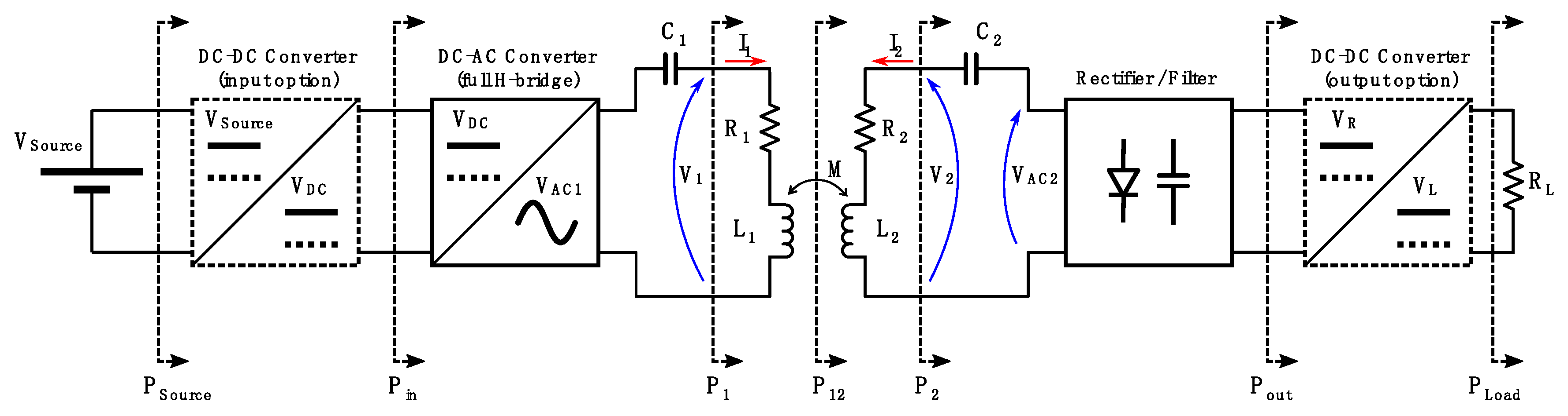
3.1. Magnetic Ressoance and the Series-Series Impedance Compensated WPT

The wireless power transfer between two magnetically coupled coils is a natural phenomenon. Electric charges, when they have their movement disturbed, induce a contrary disturbance on other nearby electric charges, as if all electric charges were solidary and concerned with keeping things unchanged in their neighborhood of the time-space continuum. This happens either with electric charges in nearby, galvanically isolated, conductive bodies, or with other charges within the very same conductor where the first charges were disturbed. The electric charges are observed to be sensitive not to the movement of other charges itself, but rather, to changes in their motion (current). This phenomenon, when referring to the interaction of charges within the same conductor is called self-inductance, and when referring to the interactions of charges in different conductor bodies, mutual inductance, and provides the mechanism for inductive WPT. In this context, magnetic resonance is achieved when circuitry coupled to both primary and secondary coils cause them to auto-resonate at the same frequency, by separately compensating the self-inductance of each of the coupled coils, and the power transfer in between primary and secondary is maximized.
The basic resonance circuit, used by Hertz, Tesla, and other early experimenters, is the same series-series resonant circuit commonly used in modern WPT equipment, with capacitors used in series with both primary and secondary coils, as shown in Figure 4.
In each loop circuit, the voltage across the capacitor is responsible for the displacement of the charges in the conductor, and this voltage increases with the integral of the charge that is being displaced along the conductor itself. Then a pair of differential linear equations of second order is created, one on the voltage and another on the current flow. The solutions for these equations, when there is no external stimulus ( v A C = 0 ), are damped harmonic (sinusoidal) functions of time, for both the capacitor voltage and the current intensity flowing in the loops. When each resonant circuit is considered alone, the resulting frequencies f n of this intrinsic oscillation of the capacitor charge and the current on each loop are such that:
ω n   =   2 π f n   = 1 L n C n   ,   n     { 1 , 2 }
If the capacitance values C i , on each side, are set so that natural oscillation frequency of both primary and secondary, when separately considered, are equal to the frequency of voltage source V A C driving the primary, currents on both coil windings will greatly increase, for a given resistive load R L , and the magnetic resonance condition is established.
As a result of the phase delay existing between the currents in these two resonant circuits, and the phase delay between each current and the voltage of its associated capacitor, the electric energy stored in the capacitors and inductors seems to be synchronously pulsing back and forth in between these coupled loops, through the magnetic field that is co-generated by the coils. If a load is attached to one the loops, it can dissipate the energy initially stored in the capacitor of the other loop, beyond that stored in its own capacitor. When v A C is connected to the primary loop at the resonant frequency, power is transferred to the secondary circuit through the magnetic link.
However, the mathematical details involved in the SS WPT configuration can be more subtle than Equation (1). If, for instance, the primary and secondary circuits have identical capacitors and inductors, thus both auto-resonate at frequency f 0 , and if R 1 can be neglected (taken as zero) when compared to | ω 0 L 1 | , then there will be a critical magnetic coupling coefficient, k s , above which the joint resonant frequency for the pair of coil resonators splits in two new frequencies different from f 0 , f o d d and f e v e n , which are given by [20]:
{ f o d d   ,   f e v e n }   =   { f 0   ( 2 1 / Q s 2 ) ± ( 2 1 / Q s 2 ) 2 4 ( 1 k 2 ) 2 ( 1 k 2 ) } ,
or, for large values of Q s , approximately:
f e v e n   1 1 k f o ,
f o d d   1 1 + k f o ,
whenever k   >   k s , where:
k s   = 1 Q s   1 1 4 Q s 2   , Q s = ω 0 L R L + R 2
Even if k   k s , the single joint resonance frequency will be slightly altered by the interaction of the two circuits, only asymptotically, as k 0 , being calculated as Equation (1).
At k = k s (the frequency split point), the resonance frequency f s is given by [20]:
f s   =   f 0   1 1 2 Q s 2
Noticeably, f s is close to, but slightly greater than f 0 , for a large value of Q s . So, when designing a SS-compensated WPT, if small values for k are adopted, magnetic resonance is always expected at a slightly higher frequency than that given by Equation (1). If k is greater than k s , as given by Equation (5), then magnetic resonance will be found at two significantly different frequencies, Equations (3) and (4), from that f 0 , calculated in Equation (1).

3.2. Estimation of the Maximum Power that Can Be Transferred over a Lossless Magnetic Link

Let ξ 1 and ξ 2 be two magnetically coupled coils, as in Figure 4, such that both their self-inductances L 1 and L 2 , and their mutual inductance, M , are constants, and their electrical serial resistances are modeled as real functions R 1 and R 2 of the frequency of the harmonic currents I ˙ 1 and I ˙ 2 , respectively exciting them. Let the lengths of ξ 1 and ξ 2 are also much smaller than the wavelength associated with the upper limit of the frequency band of interest, so no energy losses are accountable to irradiation.
In these conditions, the application of Maxwell’s Equations to these magnetically coupled coils has led to simplified models of transformers, that were extensively proved by experimentation and that can effectively allow the calculation of energy transfer over these entities with Circuit Theory. In this way, the behavior of magnetically coupled coils, as shown in Figure 4, under harmonic excitation is well described by the simplified transformer model, given by the complex Equations (7) and (8).
v 1 = L 1   t i 1 + M t i 2   ,
v 2 = L 2 t i 2 + M t i 1   ,
where, v 1 and v 2 are functions of the time expressing the voltages across the terminals of ξ 1 and ξ 2 , and similarly, i 1 and i 2 are the currents entering their reference nodes (terminals), marked in Figure 4 with dots. Again, considering these currents as sinusoidal functions of time (harmonic excitation) at a given frequency f , with ω = 2 π f , Equations (7) and (8) can be rewritten in terms of phasors, as Equations (9) and (10):
V ˙ 1 = j ω L 1   I ˙ 1 + j ω M   I ˙ 2
V ˙ 2 = j ω L 2   I ˙ 2 + j ω M   I ˙ 1
where, for k { 1 ,   2 } :
I ˙ n ( t ) = 2   I r m s n   e j ( ω t +   φ n ) , i n ( t ) = R e ( I ˙ n ( t ) )
V ˙ n ( t ) = 2   V r m s n   e j ( ω t +   θ n ) , v n ( t ) = R e ( V ˙ n ( t ) )
The power, S ˙ , transferred from ξ 1 to ξ 2 is then given by Equation (13):
S ˙ = V ˙ M 1   I ˙ 1 * 2 = V ˙ M 2   ( I ˙ 2 * ) 2 =   j ω w M   I ˙ 1 *   I ˙ 2 2   =   j ω w M   I ˙ 1   I ˙ 2 * 2   ,
The average real power P 1 , 2 transferred from ξ 1 to ξ 2 over the magnetic coupling is then given by:
P 1 , 2   = ω   M   I r m s 1   I r m s 2   sin ( φ 1 φ 2 ) ,
For fixed r m s values I r m s 1 and I r m s 2 , f and M , it can be seen that the transferred power will be positive and maximized when φ 1 φ 2 =   π / 2 , that is, when I ˙ 2 , the current entering the reference node on coil ξ 2 , has a phase delay of π / 2 , with respect to the phase of I ˙ 1 , the current entering the reference node on coil ξ 1 . This condition is met when:
I ˙ 2 =   α   j   I ˙ 1 ,   α > 0 ,
and it is equivalent to requiring the current leaving the reference node of ξ 2 to exhibit a phase advance of π / 2 , with respect to the phase of the current entering the reference node of ξ 1 , and it can be met by simply attaching a purely resistive load to a perfectly compensated secondary circuit.
The maximum power that can be transferred from ξ 1 to ξ 1 is then:
[ P 1 , 2 ] m a x   = ω   M   [ I r m s 1 ] m a x   [ I r m s 2 ] m a x
The limits on the maximum r m s currents of ξ 1 and ξ 2 are generally due to the maximum heat dissipation the coils can handle, before their wires fuse, either completely blowing out or just melting together, in case of litz wires. Other reason for limiting the currents flowing through the coils is to avoid saturation of their core, for instance, ferrites plates, if they are used in the constitution of ξ 1 or ξ 2 . If saturation occurs, peaks of current can occur, as well as increased thermal losses in the core, which will equally overheat the coils. Less often, the currents should still be limited for the reason of limiting the voltage across neighbor coil turns, what otherwise might lead to dielectric breakdown and current leakage within the coil, or from the coil to the environment.
If the coil is tailored-built according to a WPT design, all these circumstances and parameters should be carefully controlled. On the other hand, if it is a standard component to be chosen, the maximum r m s current should be verified in the coil’s specifications, or derived from their constitutional elements (wire, core, wire isolation, and geometry).
As a special case, if coils ξ 1 and ξ 2 are identical, Equation (16) simplifies to:
[ P 1 , 2 ] m a x   = ω   M   [ I r m s ] m a x 2
For instance, two identical coils, each with inductance L = 100   μ H , [ I r m s ] m a x = 10   A , in relative position such that their magnetic coupling coefficient is k = 0.2 , should be able to (wirelessly) transfer, under harmonic excitation at 100 kHz:
[ P 1 , 2 ] m a x   = 2 π   ×   100   kHz   ×   0.2   ×   100   μ H   ×   ( 10   A ) 2 = 1256   W ,
where M was calculated by the product k L = 0.2   × 100   μ H . At 50 Hz, the same coil configuration would be able to transfer only 0.63 W. That is why higher frequencies are essential to be used in WPT. However, at higher frequencies the increased dissipation due to skin and proximity effects, beyond reducing electrical efficiency, may significantly decrease the value of the maximum current that can be handled by a conductor, depending on its specific geometry.
In practical implementations, impedance compensation will not be always perfect, thus the phase delay between primary and secondary currents is not necessarily π / 2 . In fact, the impedance compensation will often be imperfect by design, because intentionally detuning the circuit helps limiting the maximum currents in the coils. So, the upper limit given by Equations (16) and (17) is unlikely to be achieved in a safe design. Similarly, in implementations where the primary is driven by a square wave generator (for instance, an H-bridge inverter), harmonic distortion can further disturb the power estimation, by affecting the relative phase of harmonic component currents in primary and secondary circuits.
Not a priori knowing the amount of detuning required in the design to limit the open secondary surge current on primary coil, a practical initial estimate for the transferred power of the circuit is obtainable considering an average value λ ¯ for λ = sin ( φ 1 φ 2 ) . That can be computed based on the heuristics of an unknown positive phase delay φ 1 φ 2 between I ˙ 1 and I ˙ 2 (i.e., I ˙ 2 lagging I ˙ 1 ) with random uniform distribution centered around the ideal value π / 2 :
λ ¯   =   1 π 0 π sin ( φ )   d φ =   2 π
Using Equations (14) and (19), in a first design approach, the estimated transferred power becomes:
P ^ 1 , 2   2 π   ω M   I r m s 1   I r m s 2   =   4 f M   I r m s 1   I r m s 2 ,
and a reasonably expectable a priori value for the maximum transferred power, in a practical WPT implementation, becomes:
[ P 1 , 2 ] m a x 4 f M   [ I r m s 1 ] m a x   [ I r m s 2 ] m a x
In this manner, the transferred power in the example given in Equation (18) would be more conservatively reduced to:
[ P 1 , 2 ] m a x   = 4   ×   100   kHz     ×     0.2   ×   100   μ H   ×   ( 10   A ) 2 = 800   W
Again, it is emphasized that Equation (21) is not a maximum theoretical limit for the transferred power, but rather, a more realistic prediction for this parameter, when the circuit is detuned from resonance. In an optimally tuned design, with no safety restrictions (concerning an open secondary), Equation (16) could be still used.

3.3. Magnetic Coupling Efficiency and the Overall DC-DC Efficiency

Usually there is a greater interest in the net power delivered to the circuit at the terminals of the load, not the gross power that is transferred over the magnetic link, as estimated by Equation (14) or Equation (21). In the same way, on perspective of the primary circuit, the power that really counts is the power delivered by the primary power source, usually of DC type.
In a typical WPT system, the power flows from the primary DC power source to the secondary load R L . Power transfer can be measured in natural boundaries of the system, as shown in Figure 5:
  • P S o u r c e 
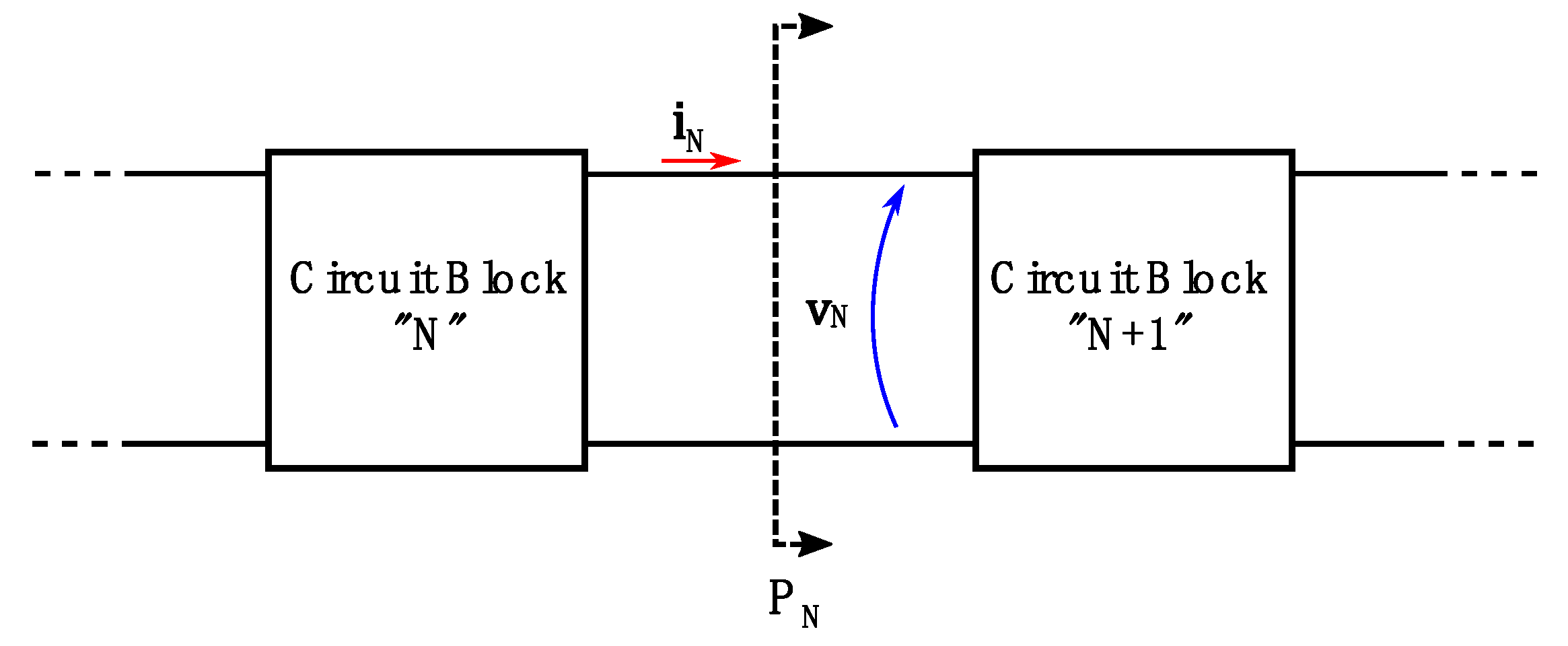
, the power supplied by the primary DC source.
  • P i n , the power supplied to the compensation circuit by the primary DC-DC converter.
  • P 1 , the power delivered at the terminals of the primary coil of the magnetic link.
  • P 1 , 2 , the power transferred over the air-gap of the magnetic link.
  • P 2 , the power delivered to the secondary circuit by the magnetic link.
  • P o u t , the power delivered to the load-matching DC-DC converter in the secondary.
  • P L o a d , the power consumed by the load, R L .
Noticeable in Figure 5, DC-DC converters, at the input and output, are optional, to help adjust and stabilize the output voltage V L , and only one of them is usually implemented in one same system. They are not necessary if the load R L does not require voltage regulation, and the output voltage V L can be directly matched by V S o u r c e and the voltage transformation of the magnetic link.
In Section 3.2, P 1 , 2 was estimated, but the power losses on the pair ( ξ 1 , ξ 2 ) were not computed. In a first approach to the estimation of losses, the windings of both ξ 1 and ξ 2 are considered to exhibit linear series resistances, which are dependent solely on the frequency of excitation, materials and geometric parameters of the coils. These resistances, respectively R 1 and R 2 , are difficult parameters to design, or even to accurately measure, in real circuit conditions, for they will depend on skin and proximity effects, which will depend not only on the nature and geometry of the conductors ξ 1 and ξ 2 , but also on the properties and geometrical distribution of the soft magnetic materials of the core, on the dielectrics that constitute their insulants and potentially, any conductive part used as magnetic shielding. If the coupling coefficient between ξ 1 and ξ 2 is significantly high, the experimental characterization of R 1 and R 2 is even more difficult, for they may vary over a wide range of currents and coupling conditions. That is, the intensity and relative phase of the current in one of the coils may affect the resistance of the other coil, fact that violates the simple linear model with fixed R 1 and R 2 . In most cases, as a simplification, this can be ignored in the models and with open secondary value of R 1 and the open primary value of R 2 being used.
To facilitate the design, usually coil manufacturers provide characteristic curves for the coil quality factor ( Q ) and inductance ( L ) , as functions of the application frequency, such that:
Q n ( f ) =   2 π f   L n ( f ) R n ( f ) , n     { 1 ,   2 }  
Then R n ( f ) can be reciprocally calculated by:
R n ( f )   =   2 π f   L n ( f ) Q n ( f ) , n     { 1 ,   2 }  
When working with a fixed frequency, it is possible to write Q 1 , Q 2 , L 1 , L 2 , R 1 , and R 2 . Then the first efficiency term that can be derived is η 1 , 2 , the magnetic link efficiency:
η 1 , 2   =   P 2 P 1
η 1 ,   2   =   P 1 , 2 R 2   ( I r m s 2 ) 2   P 1 , 2 + R 1 ( I r m s 1 ) 2   =   λ   ω M   I r m s 1 I r m s 2 ω L 2 Q 2 ( I r m s 2 ) 2   λ   ω M   I r m s 1 I r m s 2 + ω L 1 Q 1 ( I r m s 1 ) 2
At resonance, λ = sin ( φ 1 φ 2 ) = 1 , then:
η 1 , 2   =   k   ( L 1 L 2 ) 1 / 2 ( I r m s 2 I r m s 1 ) L 2 Q 2   k   ( L 1 L 2 ) 1 / 2 + ( I r m s 1 I r m s 2 ) L 1 Q 1   =   1 1 k Q 2 ( I r m s 2 I r m s 1 ) ( L 2 L 1 ) 1 / 2   1 + 1 k Q 1 ( I r m s 1 I r m s 2 ) ( L 1 L 2 ) 1 / 2
Further, if coils ξ 1 and ξ 2 are identical, with inductance L and quality factor Q, and if currents I r m s 1 and   I r m s 2 are equal, noticing that k Q > 0 , Equation (27) simplifies to:
η 1 ,   2   =   1 1 k Q   1 + 1 k Q   = 1   2 k Q +   2 k 2 Q 2   ( 1 + 1 k Q ) >   1   2 k Q
For the desirable large values of k Q , it is then possible to use the conservative estimation for the maximum η 1 , 2 :
[ η 1 ,   2 ] m a x     1 2 k Q
In the general case, whereas ξ 1 and ξ 2 are not identical, Zargham and Gulak [21] provided an expression for the maximum achievable efficiency η 1 , 2 , that should be used instead, when the quality factors of the coils are not very large, in proportion to very small coupling coefficient k :
[ η 1 ,   2 ] m a x   =   k 2 Q 1 Q 2 ( 1 + 1 + k 2 Q 1 Q 2 ) 2
When k Q 1 Q 2 is very large, Equation (30) also simplifies back to an expression that is equivalent to Equation (29):
η 1 , 2     1 2 k Q 1 Q 2
C 1 and C 2 could have been alternatively included in the central section that contains the magnetic link, as long as the serial parasite resistances of C 1 and C 2 were added respectively to R 1 and R 2 in the evaluation of new overall Q 1 and Q 2 .
Looking at Figure 5, the maximum global DC-to-DC efficiency is then computed by the product of the efficiency of each of the cascaded circuit sections:
η D C   =   P I n   P S o u r c e   P 1   P i n   P 12   P 1   P 2   P 12   P O u t P 2   P L o a d P O u t ,
η D C   =   η D C 1   η D C / A C   η 1 , 2   η R e c t f i e r   η D C 2 ,
where:
  • η D C 1 is the efficiency of the DC-DC at the input of the primary side.
  • η D C / A C is the efficiency of the DC-AC converter driving the compensation circuit of the primary side, typically in the simpler WPT system, an H-bridge inverter.
  • η R e c t f i e r is the joint efficiency of the secondary compensation, the rectifier and DC filter on the secondary side.
  • η D C 2 is the efficiency of the DC-DC converter that, if present, will feed the load.
In the best case, where a minimal circuit design can be implemented, both input and output DC-DC converters can be eliminated, and the global efficiency expressed by:
η D C   =   η D C / A C   η 1 , 2   η R e c t f i e r
Current design techniques for low power applications would result in an average efficiency of around 91–98% for each cascaded element in this composition, resulting in an overall η D C efficiency for the WPT in the range of 75–94%. Often, for low power applications, the lower boundaries of this efficiency range may be totally acceptable, especially if this comes as a trade-off for safety and convenience.

3.4. WPT–Adotped Circuits

Regarding the DC-AC converters used in the WPT, several relevant topologies can be considered. The low power requirements of a LiDAR application favor the use of a simple H-bridge converter, as illustrated in Figure 6. However, for the purpose of contextualizing the reader with more recent advances in the engineering of power converters, this section covers a few extended considerations on the subject, trying to introduce the reader to references that should be useful in more tight-requirements designs.
The selection of a specific topology must consider the WPT operation with high efficiency and high power density. The works in [22] and [23] present relevant reviews of DC-AC converters including galvanic isolation, but for applications of WPT the galvanic isolation in DC-AC converters is not a relevant aspect.
A WPT architecture based on a current-fed converter is proposed in [24], where a 420 W prototype was developed showing a maximum efficiency close to 90%. An integrated two-stage DC-AC converter is presented in [25], where a dynamic control strategy is proposed aiming to track the maximum efficiency of the high-efficiency bidirectional DC-AC converter, which was registered as 97.2% for an operating power of 3 kW. A high-efficiency DC-AC converter is proposed in [26], which is capable of operating in bidirectional mode and reaches an efficiency close to 98% for an operating power of about 1.2 kW. It is important to note that better efficiencies can be achieved for higher power DC-AC converters, as demonstrated in [27], where an efficiency of 99.1% was achieved for an operating power about of 25 kW.
Considering the requirements of a WPT system, the conventional circuit is the full-bridge DC-AC voltage-source, which is a topology constituted by two legs of switching devices. In addition to the full-bridge, the half-bridge is also a relevant circuit for applications of WPT. When compared with the full-bridge, this circuit requires less switching devices and gate drivers (and consequently lower resources of hardware and software), but the value of DC-link voltage is the double and the controllability is not as flexible as with the full-bridge (i.e., due to the voltage levels allowed). Consequently, the voltage applied to each switching device is also the double, as well as the ripple of current in the coupling filters (i.e., if the objective is to maintain the same current ripple, the coupling filter must be greater than the option with the full-bridge converter). For applications of WPT, multilevel topologies (more than three-levels) are also relevant, allowing to produce a voltage waveform with better quality and reducing the necessities of the coupling passive filters (i.e., the requirement of impedance compensation). Comparing with full-bridge and half-bridge circuits, multilevel circuits require more switching devices and gate drivers, as well as hardware and software resources, but the voltage applied to each one is more reduced when compared with the full-bridge and half-bridge circuits, allowing to define strategies to improve the efficiency. Exhaustive reviews about multilevel circuits are presented in [28] and [29]. A specific multilevel circuit is the cascade H-bridge (composed by full-bridge converters), but it requires independent DC-links; therefore, it can be applied for WPT systems, but requiring specific topologies in order to obtain the DC-link voltages. Two main types of cascade H-bridges can be found in the literature: the symmetric and the asymmetric. The symmetric cascade H-bridge use DC-link voltages with the same value, while the asymmetric cascade H-bridge uses DC-link voltages with the different values, permitting to obtain more voltage levels. The neutral-point-clamped (NPC) and the flying-capacitor are also other relevant multilevel circuits [30,31]. In addition, other multilevel circuits can be found in the literature for different applications and with different voltage levels. Some of these examples are presented in [32,33,34,35,36,37,38,39]. All the previous examples can be applied both for the primary-side and for the secondary-side, especially when it is required a bidirectional power flow operation. Moreover, a combination of two different converters can be used for the same WPT system. When the WPT system only operates in unidirectional power flow mode, the secondary side can be simplified by using an uncontrolled converter. Therefore, for the secondary side, the most conventional is the AC-DC based on the diode bridge, due to its simplicity, robustness and low cost. Figure 6 shows a full-bridge rectifier in conjunction with an H-bridge DC-AC converter to interface the power grid with the compensation circuit and transmitter coil.

4. WPT Design and Simulation

For a LiDAR equipment in automotive applications, the main design goal is to safely transfer energy to the LiDAR unit, in compatibility with the low latency, high data rate transfers of sensed 3D images to be processed by a central information system. The revolving LiDAR optics must receive energy from the vehicle in such a way that it is not mechanically blocked in its continuous revolving movement, an excellent opportunity for employing WPT. Without loss of generality, in our study case, WPT to a load at the power demand level on the order of 100 W, and a minimum electrical efficiency, η ^ m i n , of 70%, covering the LiDAR application requirements, were established.
In the mechanical analysis of the configuration, which is not addressed in this publication, small air-gap distances of approximately 3 mm were realized as adequate to implement WPT in between the LiDAR head and a vehicular fixture (VCF) to which the LiDAR is permanently connected during operation, being integrated to the body of the vehicle. Also, because this very manner of fixing the Lidar head to the VCF, although the LiDAR head can rotate, no relative movement other than rotation itself, between the LiDAR and the VCF, is expected. Thus, dynamic changes in either the mutual inductance or the self-inductances of primary and secondary coils are not expected as well, if axial symmetry is employed in the design. In this case, it is then possible to have the WPT to efficiently operate at a fixed frequency, what greatly simplifies the system design.
The actual voltage levels required for input and output, except from the point of technology of components involved, are not critical for the WPT design, due to the adoption of DC-DC converters in the WPT architecture, which can provide the voltage level adjustment to match the voltages available from the power source and required for the load. With careful design, only one of these converters, either at the input or at the output, is essentially required. So, in this simplified WPT design process, without loss of generality, the values of V S o u r c e and V L o a d will be arbitrarily fixed. The matching of the target load R L o a d and the DC power source voltage is then left to be accomplished by DC-DC level conversion.

4.1. Coil Selection

The coil selection is made based on frequency of operation and the power requirements of the application. Let us assume that our LiDAR application requires a minimum of 100 W of nominal load power. It started by fixing the design load power at P ^ L o a d = 150   W , instead, in order to accommodate, by design, possible future, non-anticipated project demands, up to 50% over the nominal target power. Then, considering a worst case 70% efficiency, it is established that required input power, P ^ S o u r c e , should be:
P ^ S o u r c e   =   P ^ L o a d η ^ m i n   214   W
Assuming that the partial efficiencies of primary and secondary circuits are approximately of the same magnitude, it is possible to produce a rough estimate for the power to be transferred over the magnetic link:
P ^ 1 , 2 =   P ^ S o u r c e   η ^ m i n =   P ^ L o a d η ^ m i n   179   W
For easy of manufacturing (less different parts in inventory, easier mechanics) the magnetic link is defined to be symmetrical, i.e., the coils ξ 1 and ξ 2 should be identical. An approximate conservative relation between the operating frequency f, the mutual inductance M between ξ 1 and ξ 2 and the maximum RMS current in their windings is then initially established, based on Equation (21):
P ^ 1 , 2     [ P 1 , 2 ] m a x     4 f   M   [ I r m s ] m a x 2
This leaves two degrees of freedom for the magnetic coupling. This uncertainty is further reduced by choosing the frequency of operation. In its technical information report J2954, SAE recommends the frequency band from 81.38 kHz to 90 kHz and a nominal frequency f S A E = 85 kHz for automotive recharging applications [40]. Being conservative about electromagnetic compatibility issues, the operation frequency of our prototype was selected in accordance with SAE J2954. The actual frequency adopted was f ^ A C   =   84.75   kHz , an integer submultiple of 13.56 MHz, the center of industrial, scientific, and medical (ISM) applications frequency band. This choice of frequency results in a required relation between the mutual inductance of the coil, M , and the RMS current it must withstand:
M . [ I r m s ] m a x 2     P ^ 1 , 2 4 f ^ A C   529   μ H . A 2
The [ I r m s ] m a x value depends on the coil constitution and the geometric configuration of nearby conductors and soft magnetic materials. It is a parameter usually provided in the technical specifications of commercially available components. So, it is the inductance value of the coil. However, both the self-inductance of a coil and the mutual inductance in a paired configuration depends strongly on the air-gap distance and must be evaluated in each specific configuration.
In order to establish an initial evaluation of the potential of the SS compensation technique for WPT in the LiDAR application, commercial off the shelf (COTS) coils were selected for the WPT circuit prototype. Their dimensions should be inscribed in the LiDAR and VCF footprint requirements. A pair of model 760308102142 coils, from Würth Elektronik, measuring approximately 55 mm × 55 mm in size, as shown in Figure 7 (extracted from the manufacturer’s datasheet), was then selected for this first conceptual electric prototype, for exceeding the minimum required M . [ I r m s ] m a x 2 , established in Equation (38), as shown in Table 1.
The required electrical efficiency of 70% is a figure often exceeded in the WPT literature, numbers close to or above 90% being typical in academic practice. Design initially concentrates on the over the air-gap efficiency. The best possible WPT efficiency over the air-gap can be predicted by using Equation (29) or Equation (30), based on the value of Q 0 of the coils, that can be retrieved from the coils specifications. Based on the graph shown in Figure 8, provided by the coil manufacturer, Q 0 = 85 is then estimated.
Thus, the best possible efficiency η 1 , 2 , working with a pair of these coils at k 0 = M 0 / L 0 is:
[ η 1 , 2 ] m a x     1 2 k 0 Q 0   =   1   2 ( 4.97 7.04 ) × 85     96.7 %
It should be emphasized, however, that this analytical prediction, given by Equation (39), refers only to the central efficiency component, as modeled by Equation (34). If the DC-AC converter in the primary circuit and the rectifier in the secondary circuit exhibit both efficiencies in the range of 91–95%, which can be considered typical for these circuits, for the low voltage and power levels of the application, then the expected maximum overall DC-DC efficiency should then lie in the range of 80–87%.

4.2. Impedance Compensation and DC Input Level

Once fixed the parameters of the coils, the next step on the design sequence is to compute de values of the capacitances C 1 and C 2 , which will determine the impedance compensation on primary and secondary coil windings. This is accomplished by first examining Equation (5) and checking whether for the given magnetic coupling coefficient, k , of the coil assembly, the resonance frequency will be split, that is, whether k >   k s . To compute k s , it is necessary first to have an estimate of Q s , based on the target minimum value of R L = 2.5 Ω and the actual circuit value of L , which is L 0 = 7.04   μ H plus the parasite inductance L ω of the wires connecting each coil to the circuit, a value that was empirically considered to be equal at primary and secondary, and estimated as L ω = 160   nH , using simulation resources:
Q s = ω 0 ( L 0 + L ω ) ( R L + R 2 ) ω 0 L R L 2 π × 84.75 × 10 3   ×   7.2 × 10 6 2.5 = 1.533
The magnetic coupling coefficient at the frequency splitting point, k s , is then estimated by Equation (5):
k s   = 1 1.533   1 1 4 × 1.533 2   0.6166
The actual coupling coefficient, k , will also be affected by parasite inductance L ω , and is found to be greater than k s , confirming the frequency splitting in the WPT circuit:
k = M 0 L 0 + L ω 0.6903
To determine the possible best values of C 1 and C 2 . which should be a priori equal, then the two possible resonant peak frequencies, f e v e n and f o d d , are alternatively forced to be equal to desired operating frequency, f ^ A C = 84.75   kHz , according to Equations (3) and (4):
f e v e n   1 1 k f o , e v e n = f ^ A C
f o d d   1 1 + k f o , o d d = f ^ A C  
Two possible values for f o are then derived:
f o = f o , e v e n   f ^ A C   1 k = 47.16   kHz
f o = f o , o d d   f ^ A C   1 + k = 110.2   kHz
So, based on Equation (1), if operating over the f o , e v e n peak, the value for capacitances C 1 and C 2 should be calculated as:
C q , e v e n = 1 ( L 0 + L ω ) ( 2 π   f o , e v e n ) 2 1.58   μ F , q     { 1 , 2 }
Otherwise, if operating over the f o , o d d peak,
C q , o d d = 1 ( L 0 + L ω ) ( 2 π   f o , o d d ) 2 290   nF , q     { 1 , 2 }
Adopting C q = C q , e v e n =   1.58   μ F is the most favorable design option, because it renders an inductive impedance to be fed by H-bridge inverter, while C q , o d d yields a capacitive impedance, when set in series with the primary total inductance L 0 + L ω . So, the a priori design capacitance for C 1 and C 2 is 1.58   μ F , which is rounded to the nominal value of 1.6   μ F .
With all passive components of primary and secondary circuits now determined, simulations were used to establish the required the DC power source voltage that would yield the target input power P ^ S o u r c e . The voltage of 23.6 V (nominally 24 V) was then identified, by observing circuit power values while sliding the power source voltage. This could have been done analytically, but the with all but one circuit parameter determined, simulation interaction is a practical and easier task.

4.3. Open Secondary Safety Check

When using the simple series-series (SS) compensation with a fixed power frequency, the high electrical efficiency is achieved by means of a very good resonance matching at both primary and secondary coils. This tends to cause an overloading problem in the primary, when the load is reduced well below its nominal level, or even disconnected from the secondary winding. This can damage the primary coil and its driving circuits, or even overheat nearby metallic elements, in all cases, a fire being possibly started, due to increase in temperature.
So, of central importance to the design, it is necessary to verify that the primary circuit is sufficiently detuned at open secondary condition, so that the maximum primary current at this operation point is limited to the maximum acceptable peak current specified by the coil manufacturer (and supported by primary driver circuit design). This shall provide the ability to work with simplified fixed-gap, fixed-frequency configuration, while permitting the load to totally vary from maximum to zero without compromising the primary circuit.
For tightly coupled resonant circuits ( k >   k s ), like this prototype, the frequency splitting phenomena may help to handle the open secondary condition, because the resonant frequency changes when the secondary is not coupled. Effectively, for C 1 = 1.6   μ F , at open secondary the new resonant frequency of primary circuit is:
f o p e n   s e c = 1 2 π ( L 0 + L ω ) C 1 46.9   kHz   ,  
which is well below the frequency of operation, f ^ A C = 84.75   kHz .
Circuit simulations were carried out to check if, under no load condition, the primary current would be keep limited to the maximum possible value (18 A). That was verified for any C 1 ≥ 0.9 μF. In normal operation, it was additionally observed that reducing C 1 up to 1.4 μF would still keep the peak primary current value limited to 18 A. At the same time, it was noticed that a value for C 1 slightly smaller than the previously computed 1.6 μF, while increasing the output power, did not significantly impair the electrical efficiency, which was kept in the range of 80.5–81.5%. As a result of that, the design value for C 1 was instead fixed at 1.4 μF, for which a better matching adjustment for C 2 was 1.5 μF.
The main circuit design parameters are summarized in Table 2. After an initial estimation of the over the air-gap efficiency from Equation (39), the DC-DC overall peak efficiency was derived by simulation, at the required maximum possible load (minimum possible value for R L ). In the simulation, standard components for primary DC-AC inverter and secondary rectifier were considered, being of special importance the transistors used to implement the H-bridge inverter, the Infineon IPA126N10N3G, where the drain-source on-state resistance R D S ( O N ) , m a x = 12.6   m Ω .

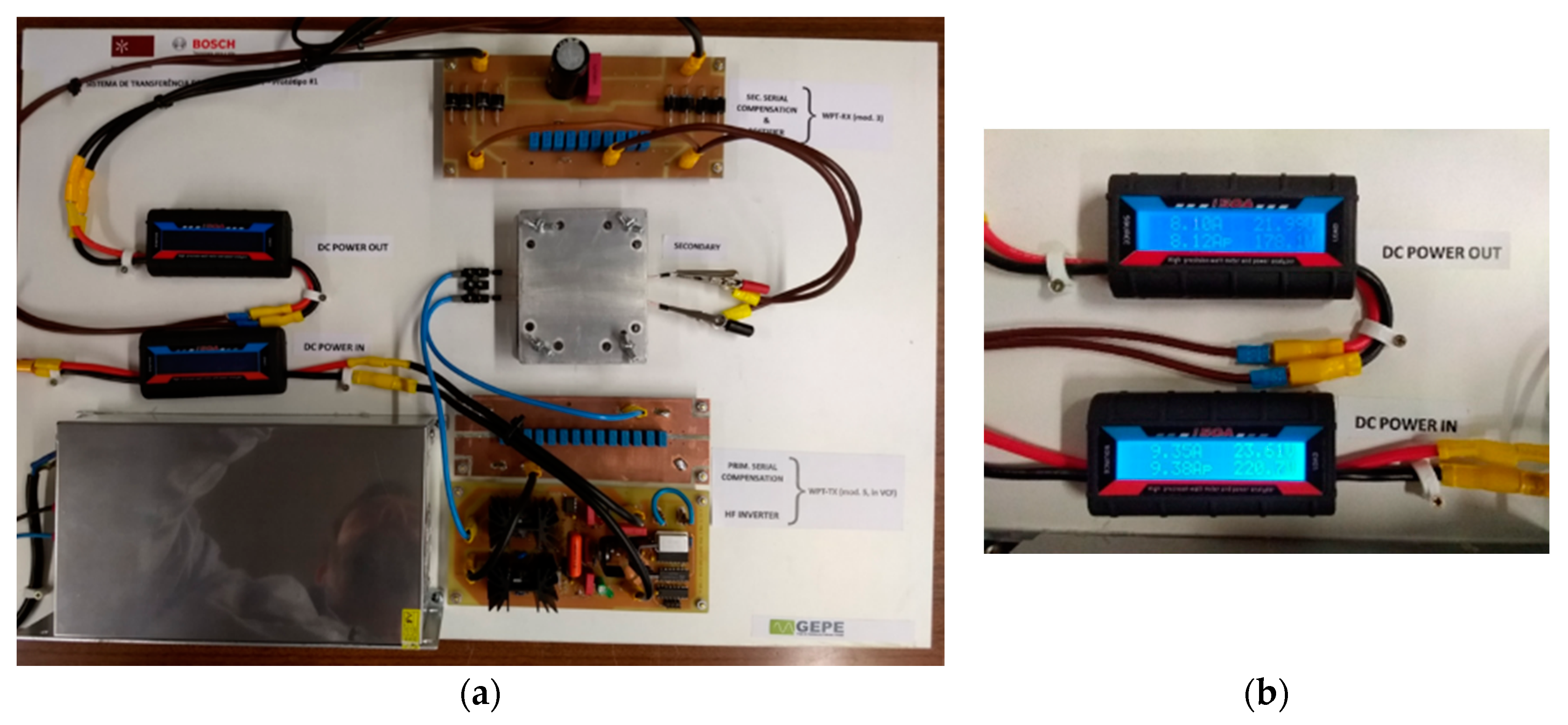
5. Results from Prototype

For didactic purposes, this first prototype implemented was totally modular, with secondary not revolving. The main module involved is the coil stack, which is the air-gapped transformer, where the primary and secondary coils are separated by a 3 mm think acrylic sheet, as shown in Figure 9.
All the modules, except the DC load, R L , were fixed on a white board, as shown in Figure 10a. The metallic box on the bottom-left is the DC power source. On the right side, from bottom to the upper border of the board are visible: The DC-AC converter Printed Circuit Board (PCB), the capacitor bank implementing C 1 ( 14 × 100   nF ) , the coil stack, closed with aluminum sheet shields, and a PCB integrating the capacitor bank implementing C 2 ( 10 × 150   nF ) and the Schottky diode full bridge rectifier. Detailed specification of components was not in the scope of this report, which is focused on WPT design and verification.
Once powered up, with an attached fixed load R L = 2.71   Ω , the waveforms of primary and secondary voltages, primary and secondary currents showed-up and where recorded as in Figure 11, resulting in the DC power readings shown in Figure 10b.
Although no thermal load evaluation was yet performed, the circuit components were verified to run just warm, at maximum load, except of course, the load R L itself, not shown in Figure 10a. The excess power over the design 150 W target was due to post-design adjustments in C 1 and C 2 , for an appealing power demonstration, that did not significantly affect the efficiency.

5.1. Output Power and Overall Efficiency

The total net output power, the input power and their ratio are possibly the easiest figures of merit to be measured and, because of that, they are mostly used by authors, when characterizing the WPT configuration at application perspective. Both the power and efficiency will vary according to the load R L that is connected at the system output.
The system design is optimized for a higher efficiency at nominal over the air-gap power level of 200 W. The design is verified by experimentally measuring the output power and efficiency for a range of load values and the resulting curves are shown in Figure 12.
A maximum efficiency of 81.5% is found at R L = 2.55   Ω , the point at which the output DC power is approximately 184 W, the input power is 225 W, and the power transferred over the air-gap should correspond approximately to 200 W. When R L < 2.5   Ω , the condition shown in the red threads of curves in Figure 12, the maximum recommended instantaneous value for the primary current (18 A) is exceeded, and the system start to operate in overload. The overload condition was tested up to the maximum output power of 300 W, when the coils’ heat dissipation is increased to sill acceptable levels, since the aluminum shield also function as a heat sink for the coils. For the prototyped configuration, operation for limited time (2 min) in this overload condition produced no permanent damage. The primary and secondary currents remained below the saturation level (30 A) in all overload range. Some points of the power curve are also corresponded on Table 3.
If an optional DC-DC converter is to be used to match a specific load voltage or current, then the characteristic curves from data in Figure 12, should provide enough information for the design of this DC-DC converter. The maximum efficiency will always be limited to the best possible value achievable by the basic system, before the insertion of the DC-DC converter.

5.2. Open Secondary Safety Check

This is a simple but important confirmatory test, realized by measuring the primary current with the oscilloscope when the secondary load has been disconnected. In Figure 13a, it may be observed that the current (CH1, yellow signal) is below 15 A, as predicted by the simulation (using PSIM software) shown in Figure 13b. In both screen-prints, measurement, and simulation, the vertical scales are the same and the colors of the channels corresponds to the same signals: I 1 (yellow), V 1 (blue), I 2 (magenta, always zero, due to open secondary), and V 2 (green), and vertical scales are the same.
During prototype tests, the peak primary current under normal operation was also verified to be less than the allowed maximum value, for all accepted load values range ( R L 2.5   Ω ), as shown in Table 3.

5.3. Power Transferred over the Air-Gap

The measurement of power at the boundaries indicated in Figure 5 permits to compute all efficiency indicators of the circuit. Each power P N , being transferred in between consecutive circuit blocks, can be estimated by averaging in time the product v N ( t p )   i N ( t p ) , as in Equation (50), with v N and i N probed as indicated in Figure 14:
P N   =   1 P p = 1 P   v N ( t p )   i N ( t p )
Measuring P S o u r c e and P L o a d are easy tasks, because the voltages and currents at these external boundaries are essentially DC levels. To estimate de power transmission efficiency over the air-gap, P 1 and P 2 could be directly measured, then η 1 , 2 could be derived by Equation (25). However, when trying to directly measure P 1 or P 2 , some practical difficulty may arise, as explained in the next paragraphs.
The series inductances of the circuit naturally filter the currents i 1 and i 2 passing through them. On the other hand, because the most common DC-AC converters used to excite the primary circuit are H-bridge, hard switching types, v 1 and v 2 tend to have high frequency components at the switching times. This can be noticed in the actual voltage waveforms (red and green curves) sampled from the prototype, shown in Figure 11, which are already filtered with a 5 MHz low-pass bandwidth.
Since the design target efficiencies for η 1 , 2 are close to the unity, P 1 and P 2 will often have very close values to each other, and any estimation error in their measurements may lead to a poor estimation of the loss P 1 P 2 . So, in practice, in order to have good precision in the numerical integration of the product v N   i N , it is necessary to use instrumentation with a sampling rate (and bandwidth) much greater the twice the highest frequency component in the measured voltages. Such equipment may not be always readily available. Beyond that, because the terminals of the mutual inductance of the model is not accessible to direct measurements of voltage, it is neither possible to directly measure P 12 , the power transferred of the air-gap, using Equation (50).
In this way, the estimation of the critical parameters   P 1 , P 12 , and P 2 , necessary for an evaluation of the winding losses and the electrical efficiency of the magnetic coupling, require some workarounds. It is possible to first estimate P 12 , instead, indirectly, by individually applying Equation (14), to each harmonic component of the power, and adding up the transferred power terms at each harmonic frequency. As Equation (14) only requires the measurement of currents entering the primary and secondary coils, which are well-conditioned signals, enhanced precision in the estimation of P 12 can be achieved.
In this method, it is necessary to start with simultaneously sampling currents i 1 and i 2 at a frequency that is greater (for more precise results, ten times greater) than twice the frequency of the highest harmonic at which some significant energy is still expected. As a result of noise in the measurements, to increase accuracy the sampling of the assumedly periodic currents i 1 and i 2 may be taken over by N consecutive periods. If, at the required sample rate, one period corresponds to P samples, then N P samples from each of these currents are acquired.
The Discrete Fourier expansion of { i 1 ( p   Δ t ) } and { i 2 ( p   Δ t ) } , for 0 p P 1 :
i q ( p Δ t )   =   n = 0 P 1   ( a q , n   cos ( n ω 1   p Δ t ) +   b q , n   sin ( n w ω 1   p Δ t ) ) , q     { 1 ,   2 }
where, for reduction of noise in   i q , the coefficients a n and b n are estimated over M periods:
a q , n   =   2 N P p = 0 N P 1   i N ( p Δ t )   cos ( n ω 1   p Δ t ) , for   1     n     P 1
b q , n   =   2 N P p = 0 N P 1   i N ( p Δ t )   sin ( n ω 1   p Δ t ) , for   1     n     P 1
and, as both i 1 and i 2 have no DC component in permanent regimen,
a q , 0   =   b q , 0   =   0
or equivalently:
i q ( p Δ t )   =   n = 1 P   h q , n sin ( n ω 1   p Δ t + φ n )
where, for q     { 1 ,   2 } :
h q , n   =   ( a q , n 2 + b q , n 2 ) 1 2
φ q , n   =   atan 2 ( b q , n , a q , n ) ,
where the function atan 2 , taking two arguments, is the four-quadrant version of the function tan 1 , the inverse tangent function.
Working with the sample period of Δ t = 10   ns and, due to memory limitations of the acquisition system, N = 2 , then the two periods of current signals i 1 and i 2 , at the fundamental frequency f ^ A C   =   84.75   kHz , corresponds to 2360 sampled points. In Figure 15, the Fourier expansions of the currents over the two consecutive periods, up to the 5th harmonic, can be seen and visually compared to the actual currents i 1 and i 2 .
The total power transferred over the air-gap, under the assumption that magnetic saturation in both primary and secondary coils is not observed, will be the signed sum of all power components at each harmonic frequency, each of them computed as in Equation (14), is given by:
P 1 , 2   =   n = 1 P P 1 , 2 ( n )   =     M 2 n = 1 P n ω 1 h 1 , n   h 2 , n   sin ( φ 1 , n φ 2 , n )
Since the very high harmonics have low power contribution, P 1 , 2 can be safely estimated by truncating the sum in Equation (58) to the first H < P terms. Using the measured value of M , as given in Table 1, then the computed power estimation of P 1 , 2 was evaluated as presented in Table 4.
The relative spectral composition of the power wirelessly transferred over the air-gap can then be better visualized in Figure 16. Noticeable, the odd harmonics, higher than the first, were measured as negative power components (plotted in red in Figure 16). That is, in these harmonics, the power is apparently flowing backwards, from the secondary coil to the primary coil, thus slightly diminishing the net WPT power.
The total harmonic distortion (THD), computed from measured signals, was 4.4% for the primary current i 1 and 6.6% for the secondary current i 2 . Circuit simulations indicated that a carefully manual adjustment of the value of capacitors C 1 and C 2 around the nominal value of 1.6 μF, which has not been accomplished, could have reduced the primary THD to at least 3.5%, not having significant impact on the reduction of the secondary THD.

5.4. Power and Efficiency Analysis

In the WPT circuit implemented in this work, a simplification was initially adopted by leaving out of the prototype all DC-DC converters that would provide the source and load matching. For an initial study, without loss of generality, both target design voltages for the DC power source and the load were nominally set at 24 V. The measured and estimated power levels at circuit boundaries, defined in Figure 5, can then be simplified to those present in Figure 17.
In Section 5.1 and Section 5.3, the values of P S o u r c e = 220.7 W, P 12 =   197.15 W, and P L o a d =   178.1 W were derived from measurements at nominal operation, i.e., at R L = 2.71   Ω . Next, P 1 and P 2 can be estimated based on previously measured values of R 1 , R 2 , that were measured at 50 mΩ (coil series resistance) plus 4 mΩ (capacitors bank series resistance), fitted at 60 mΩ with the use of simulation tools (PSIM), to include other losses in cabling, and the values of I r m s 1 and I r m s 2 , that were measured during normal operation:
P 1   =   P 1 , 2 + R 1 ( I r m s 1 ) 2   =   197.15 + 60.10 3 ( 12.9 ) 2   =   207.1   W
P 2   =   P 1 , 2 R 2 ( I r m s 2 ) 2   =   197.15 60.10 3 ( 9.47 ) 2   =   191.8   W
The electrical efficiency over the air-gap is then computed as:
η 1 ,   2 =   P 1 , 2 R 2   ( I r m s 2 ) 2   P 1 , 2 + R 1 ( I r m s 1 ) 2   = 191.8   W 207.1   W     92.6 %  
And the primary and secondary efficiencies, respectively associated with the circuits of the DC-AC converter (H-bridge) and the passive rectifier used in the design are given by:
η D C / A C =   P 1   P S o u r c e   =   207.1   W   220.7   W     93.8 % ,
η R e c t f i e r   =   P L o a d   P 2     =   178.1   W   191.8   W     92.9 %
The total DC-DC efficiency obtained is then expressed by the product in Equation (34):
η D C =   η D C / A C   η 1 , 2   η R e c t f i e r   =   93.8 % × 92.6 % × 92.9 %     80.7 %
While the output power successfully achieved the minimum target value of 150 W, exceeding it by approximately 18.7%, the WPT efficiency over the air-gap η 1 , 2 was about 4% less than the best possible predicted value for the coil configuration adopted (39). This loss can be greatly attributed to a non-optimized cable routing, using non-litz cabling to connect the terminals of the primary and secondary coils of this first prototype to their respective circuits. The efficiencies of the primary DC-AC converter and secondary rectifier were not theme of special design control, and their resulting efficiency values, typical for these types of circuits, can be improved in a follow up design.

6. Conclusions

The SS-compensated architecture is widely used in inductive wireless power transfer (WPT). A design procedure was presented, reconstructed from previously developed theory, which is valid when the application favors the use of a fixed frequency, such as in the case of fixed magnetic coupling between primary and secondary coils. The procedure was exemplified in the construction and test of the prototype of a WPT subsystem for an automotive LiDAR unit, but its guidelines are expected to fit other similar low power applications.
Due to large number of free parameters in a WPT circuit, some heuristic concerning the average attainable phase delay between primary and secondary currents was introduced, simplifying the design task, but still approximately leading to the target wirelessly transferred power. The no load condition, which is often an issue in SS-compensated WPT, is safely handled without the need for frequency agility. The electrical efficiency obtained in the process is lower than that that would be possibly achievable in an optimum design, but still, it can be accepted in a low power application.
A robust method of measuring the power transferred over the air-gap (Section 5.3), based on simultaneous measurements of primary and secondary currents, and Fourier spectral analysis, was used to evaluate the power transferred at the air-gap, and then the primary input and secondary output power. After partial circuit efficiencies are estimated using Equation (64), it becomes evident that the major factor affecting the overall efficiency are: (i) the simple rectification circuitry used in the prototype, with an efficiency of approximately 93%; (ii) the energy lost in cabling and connections, and the choice of a non-optimal pair of coils, considering the operation frequency adopted, altogether resulting in about 93% efficiency; and (iii) the technology of the DC-AC converter, with about 94% of efficiency. These efficiency numbers indicate that some improvement on the overall efficiency, without changing the WPT configuration, is expected only by replacing the secondary passive diode bridge rectification block, by a more advanced configuration, namely, a synchronous rectifier. The losses in cabling are expected to be greatly reduced when the circuit is packed into a new dedicated PCB. Also remarkable, commercial off the shelf (COTS) inductors were used in the implementation, which, despite of being products of high quality and value, are not optimized (best Q-factor) for use at the relatively low arbitrated transmitting frequency f S A E . Thus, if f S A E is to be kept, a new custom-made pair of coils, with higher Q-factor at this frequency, should conquest a few percent increase in efficiency. Otherwise, careful electromagnetic compatibility analysis in the application environment needs to be carried out, to help evaluate the possibility of safely abandoning f S A E for higher WPT frequencies.
Last, in this first prototype, without loss of generality, all DC-DC converters were suppressed from the original architecture, so that load match was not of concern. A final design integrating at least one DC-DC converter at the output of the rectification circuit block should match the voltage and load specified by application, at the expense of a few percent extra loss in efficiency.

Author Contributions

L.A.L.C. and V.M. performed the tasks associated with formal analysis, circuit design, and testing, and the writing—original draft preparation. All the authors participated in the conceptualization, methodology, and writing—review and editing. All authors have read and agreed to the published version of the manuscript.

Funding

This work has been supported by national funds through FCT—Fundação para a Ciência e Tecnologia within the Project Scope: UID/CEC/00319/2019, and also European Structural and Investment Funds in the FEDER component, through the Operational Competitiveness and Internationalization Programme (COMPETE 2020) [Project nº 037902; Funding Reference: POCI-01-0247-FEDER-037902].

Acknowledgments

The authors would like to express their gratitude to José Maia C. Cunha, who helped in the verification of measurements in the prototype. The authors would like to thank the MSc Thesis developed by Joaquim Santos (Proof-of-concept of a Single-point Time-of-Flight LiDAR System and Guidelines towards Integrated High-accuracy Timing, Advanced Polarization Sensing and Scanning with a MEMS Micromirror), developed under a partnership between Bosch Car Multimedia and the University of Minho, which was useful to write part of the section 2.1.

Conflicts of Interest

The authors declare no conflict of interest.

References

  1. Maxwell, J.C. A Treatise on Electricity and Magnetism, 3rd ed.; 1891; Dover Publications, Inc.: New York, NY, USA, 1873. [Google Scholar]
  2. Mulligan, J.F. Heinrich Hertz and the development of physics. Phys. Today 1989, 42, 50–57. [Google Scholar] [CrossRef]
  3. Helrich, C.S. The Classical Theory of Fields, 1st ed.; Needs, R., Rhodes, W.T., Stanley, H.E., Eds.; Springer: Berlin/Heidelberg, Germany, 2012. [Google Scholar]
  4. The Faraday centenary—A supplement to the bell system. Tech. J. 1931, 10, i–vii.
  5. Faraday, M. Experimental Researches in Electricity, 2nd ed.; 1849; Richard, E., John, E., Eds.; Richard and John Edward Taylor, Printers and Publishers to the University of London: London, UK, 1839; Volume 1. [Google Scholar]
  6. Coltman, J.W. The transformer historical overview. IEEE Ind. Appl. Mag. 2002, 8, 8–15. [Google Scholar] [CrossRef] [Green Version]
  7. Leyh, G.E.; Kennan, M.D. Efficient wireless transmission of power using resonators with coupled electric fields. In Proceedings of the 2008 40th North American Power Symposium, Calgary, AB, Canada, 28–30 September 2008; pp. 1–4. [Google Scholar]
  8. Tesla, N. Nikola Tesla on His Work With Alternating Currents and Their Application to Wireless Telegraphy, Telephony, and Transmission of Power—An Extended Interview (Tesla Presents Series, Part 1); Anderson, L.I., Ed.; Twenty First Century Books: Breckenridge, CO, USA, 1992. [Google Scholar]
  9. Kurs, A.; Karalis, A.; Moffatt, R.; Joannopoulos, J.D.; Fisher, P.; Soljačić, M. Wireless power transfer via strongly coupled magnetic resonances. Science 2007, 317, 83–87. [Google Scholar] [CrossRef] [Green Version]
  10. Boys, J.T.; Covic, G.A. The inductive power transfer story at the University of Auckland. IEEE Circuits Syst. Mag. 2015, 15, 6–27. [Google Scholar] [CrossRef]
  11. Lidar, V. Velodyne’s HDL-64E: A high definition LiDAR sensor for 3D applications; White Paper—Velodyne LiDAR: San Jose, CA, USA, 2007; pp. 1–7. [Google Scholar]
  12. Varshney, L.R. Transporting information and energy simultaneously. In Proceedings of the 2008 IEEE International Symposium on Information Theory, Toronto, ON, Canada, 6–11 July 2008; pp. 1612–1616. [Google Scholar]
  13. Liu, L.; Zhang, R.; Chua, K. Wireless information transfer with opportunistic energy harvesting. IEEE Trans. Wirel. Commun. 2013, 12, 288–300. [Google Scholar] [CrossRef] [Green Version]
  14. Perera, T.D.P.; Jayakody, D.N.K.; De, S.; Ivanov, M.A. A Survey on simultaneous wireless information and power transfer. J. Phys. Conf. Ser. 2017, 803, 012113. [Google Scholar] [CrossRef]
  15. Berger, A.L.; Pilnick, B. Interface for Transferring Power and Data Between a Non-Rotating Body and a Rotating Body. World Intellectual Property Organization. U.S. Patent No. WO 2018/125709 Al, 5 July 2018. [Google Scholar]
  16. Worms, K.; Dreschmann, M. Lidar System, Operating Method for a Lidar Syetem and Working Device. Weltorganisation für Geistiges Eigentum. U.S. Patent No. WO 2019/158301 Al, 4 April 2019. [Google Scholar]
  17. Wu, M.C.; Lin, C.H.; Fang, M.H. Rotating Optical Range Finder. United States Patent Application Publication. U.S. Patent US 2016/0274221 A1, 22 September 2016. [Google Scholar]
  18. Pacala, A.; Yu, T.; Eldada, L. Cost-Effective Lidar Sensor for Multi-Signal Detection, Weak Signal Detection and Signal Disambiguation and Method of Using Same. U.S. Patent US20140211194A1, 31 July 2014. [Google Scholar]
  19. Hall, D.S. High definition LiDAR system. U.S. Patent US8767190B2, 1 July 2014. [Google Scholar]
  20. Niu, W.; Chu, J.; Gu, W.; Shen, A. Exact analysis of frequency splitting phenomena of contactless power transfer systems. IEEE Trans. Circuits Syst. I Regul. Pap. 2013, 60, 1670–1677. [Google Scholar] [CrossRef]
  21. Zargham, M.; Gulak, P.G. Maximum achievable efficiency in near-field coupled power-transfer systems. IEEE Trans. Biomed. Circuits Syst. 2012, 6, 228–245. [Google Scholar] [CrossRef]
  22. Singh, B.; Singh, S.; Chandra, A.; Al-Haddad, K. Comprehensive study of single-phase ac-dc power factor corrected converters with high-frequency isolation. IEEE Trans. Ind. Inform. 2011, 7, 540–556. [Google Scholar] [CrossRef]
  23. Bellar, M.D.; Wu, T.S.; Tchamdjou, A.; Mahdavi, J.; Ehsani, M. A review of soft-switched DC-AC converters. IEEE Trans. Ind. Appl. 1998, 34, 847–860. [Google Scholar] [CrossRef]
  24. Samanta, S.; Rathore, A.K. Wireless power transfer technology using full-bridge current-fed topology for medium power applications. IET Power Electron. 2016, 9, 1903–1913. [Google Scholar] [CrossRef]
  25. Mallik, A.; Khaligh, A. Maximum efficiency tracking of an integrated two-staged AC–DC converter using variable DC-link voltage. IEEE Trans. Ind. Electron. 2018, 65, 8408–8421. [Google Scholar] [CrossRef]
  26. Qian, H.; Lai, J.; Zhang, J.; Yu, W. High-efficiency bidirectional AC-DC converter for energy storage systems. In Proceedings of the 2010 IEEE Energy Conversion Congress and Exposition, Atlanta, Georgia, 12–16 September 2010; pp. 3224–3229. [Google Scholar]
  27. Rothmund, D.; Guillod, T.; Bortis, D.; Kolar, J.W. 99.1% efficient 10 kV SiC-based medium-voltage ZVS bidirectional single-phase PFC AC/DC stage. IEEE J. Emerg. Sel. Top. Power Electron. 2019, 7, 779–797. [Google Scholar] [CrossRef]
  28. Lai, J.-S.; Peng, F.Z. Multilevel converters-a new breed of power converters. IEEE Trans. Ind. Appl. 1996, 32, 509–517. [Google Scholar]
  29. Rodriguez, J.; Lai, J.-S.; Peng, F.Z. Multilevel inverters: A survey of topologies, controls, and applications. IEEE Trans. Ind. Electron. 2002, 49, 724–738. [Google Scholar] [CrossRef] [Green Version]
  30. Park, S.-J.; Kang, F.-S.; Lee, M.H.; Kim, C.-U. A new single-phase five-level PWM inverter employing a deadbeat control scheme. IEEE Trans. Power Electron. 2003, 18, 831–843. [Google Scholar] [CrossRef]
  31. Marchesoni, M.; Mazzucchelli, M.; Tenconi, S. A non conventional power converter for plasma stabilization. In Proceedings of the PESC ’88 Record: 19th Annual IEEE Power Electronics Specialists Conference, Kyoto, Japan, 11–14 April 1988; Volume 1, pp. 122–129. [Google Scholar]
  32. Khoucha, F.; Lagoun, M.S.; Kheloui, A.; Benbouzid, M.E.H. A comparison of symmetrical and asymmetrical three-phase H-bridge multilevel inverter for DTC induction motor drives. IEEE Trans. Energy Convers. 2011, 26, 64–72. [Google Scholar] [CrossRef] [Green Version]
  33. Zhang, L.; Sun, K.; Feng, L.; Wu, H.; Xing, Y. A Family of neutral point clamped full-bridge topologies for transformerless photovoltaic grid-tied inverters. IEEE Trans. Power Electron. 2013, 28, 730–739. [Google Scholar] [CrossRef]
  34. Teixeira, C.A.; Holmes, D.G.; McGrath, B.P. Single-Phase Semi-Bridge Five-Level Flying-Capacitor Rectifier. IEEE Trans. Ind. Appl. 2013, 49, 2158–2166. [Google Scholar] [CrossRef]
  35. Ahmed, R.A.; Mekhilef, S.; Ping, H.W. New multilevel inverter topology with minimum number of switches. In Proceedings of the TENCON 2010: 2010 IEEE Region 10 Conference, Fukuoka, Japan, 21–24 November 2010; pp. 1862–1867. [Google Scholar]
  36. Buticchi, G.; Barater, D.; Lorenzani, E.; Concari, C.; Franceschini, G. A nine-level grid-connected converter topology for single-phase transformerless PV systems. IEEE Trans. Ind. Electron. 2014, 61, 3951–3960. [Google Scholar] [CrossRef]
  37. Liu, J.; Cheng, K.W.E.; Ye, Y. A cascaded multilevel inverter based on switched-capacitor for high-frequency AC power distribution system. IEEE Trans. Power Electron. 2014, 29, 4219–4230. [Google Scholar] [CrossRef]
  38. Babaei, E.; Alilu, S.; Laali, S. A new general topology for cascaded multilevel inverters with reduced number of components based on developed H-bridge. IEEE Trans. Ind. Electron. 2014, 61, 3932–3939. [Google Scholar] [CrossRef]
  39. Babaei, E.; Laali, S.; Alilu, S. Cascaded multilevel inverter with series connection of novel H-bridge basic units. IEEE Trans. Ind. Electron. 2014, 61, 6664–6671. [Google Scholar] [CrossRef]
  40. Society of Automobile Engineers (SAE). SAE Technical Information Report J2954—Wireless Power Transfer for Light-Duty Plug-In/Electric Vehicles and Alignment Methodology; SAE: Warrendale, PA, USA, 2016. [Google Scholar]
Figure 1. Basic diagram about how light detection and ranging (LiDAR) technology works.
Electronics 09 00086 g001
Figure 2. Example of a LiDAR sensor capable of 360° viewing angle working in constant rotation.
Electronics 09 00086 g002
Figure 3. System architecture diagram, emphasizing wireless power transfer (WPT) implementation and wireless information transfer (WIT).
Electronics 09 00086 g003
Figure 4. Two magnetically coupled resonant loops using series-series compensation.
Electronics 09 00086 g004
Figure 5. Typical series-series (SS)-compensated WPT system architecture, sectioned at power transfer boundaries.
Electronics 09 00086 g005
Figure 6. Full-bridge rectifier in conjunction with an H-bridge DC-AC converter to interface the power grid with the compensation circuit and transmitter coil.
Electronics 09 00086 g006
Figure 7. Dimensions (mm) of the commercial off the shelf (COTS) coils used in the design (Würth Elektronik 760308102142).
Electronics 09 00086 g007
Figure 8. Q-factor of selected coil as a function of frequency of operation (from Würth Elektronik).
Electronics 09 00086 g008
Figure 9. Coil stack used in the 150 W WPT prototype: (a) Photo, partially disassembled; (b) Stack cross section schematics.
Electronics 09 00086 g009
Figure 10. (a) First conceptual prototype of the WPT subsystem of the LiDAR, achieving more than 175 W at 80.5% efficiency. (b) Approximate input and output power readings, using DC power meters.
Electronics 09 00086 g010
Figure 11. Experimental results of voltages and currents waveforms on the terminals of primary and secondary coils.
Electronics 09 00086 g011
Figure 12. Experimental results of the output power and base overall DC efficiency as a function of R L (in logarithmic scale).
Electronics 09 00086 g012
Figure 13. Testing the open secondary load exception: (a) Screen-print of the oscilloscope; (b) Print screen of simulation with PSIM software. Same channels in (a,b), which corresponds to the same signals.
Electronics 09 00086 g013
Figure 14. Measurement of power P N crossing boundary in between two consecutive circuit blocks.
Electronics 09 00086 g014
Figure 15. Fourier expansions of measured currents in primary and secondary coils, trunked to the 5th harmonic.
Electronics 09 00086 g015
Figure 16. Spectral composition of WPT power over the air-gap, referenced to the first order harmonic.
Electronics 09 00086 g016
Figure 17. Power transfer boundaries in the simplified schematic of the implemented circuit.
Electronics 09 00086 g017
Table 1. Coil selection and validation.
Component SpecificationMeasured Values * (gap = 3 mm)Energy ParameterEstimated Transferrable Power @ f ^ AC
Coil ModelL (self-inductance) I max (A) L 0 (μH) M 0 (μH) M . [ I rms ] max 2 (μH.A2)(W)
Würth Elektronik 7603081021425.8 ± 10%187.04 ± 2%4.97 ± 2%805 ± 10% (coil model)273 ± 10% (coil model)
* Sample paired coils: The self-inductance of a coil is increased due to the proximity of another coil.
Table 2. Main WPT design parameters.
ParameterDesign Value
Air-gap, d3 mm
Frequency of Operation, f ^ A C 84.75 kHz
CoilStand Alone Inductance, L 5.8 μH
Coupled Leakage Inductance, L 1 =   L 2 7.04 μH
Mutual Inductance, M 4.97 μH
Q-factor @ f ^ A C , Q 1 85
Primary compensation capacitor, C 1 1.4 μF
Secondary compensation capacitor, C 2 1.5 μF
Primary DC power source, V S o u r c e 24 V
Load resistance, R L ≥2.5 Ω
Maximum DC load power, P ^ L o a d ≥150 W
DC-DC overall peak efficiency, η ^ D C ≥80%
Over the air-gap peak efficiency, η ^ 1 , 2 ≤96.7%
Table 3. Main system’s input and output power values.
R L   ( Ω ) P S o u r c e
Input Power (W)
Peak Primary Current (A) P L o a d
Output Power (W)
Overall DC Efficiency (%)
1.19 ∗395.227.6300.476.2
2.55225.717.8184.081.5
2.71220.717.4178.180.7
3.16193.816.4154.879.9
4.57149.614.5114.376.4
7.86100.413.170.870.5
16.163.413.336.454.6
∗ Overload condition. Tested for 2 min continuously.
Table 4. Estimation of P 1 , 2 , the power transferred over the air-gap.
n P 1 , 2 ( n )   ( in   Watts ) 10 log 10 ( | P 1 , 2 ( n ) | | P 1 , 2 ( 1 ) | )   ( in   dB ) k = 1 n P 1 , 2 ( k )   ( in   Watts )
1199.1560980199.16
20.090544−33.4199.25
3−1.694581−20.7197.55
40.013378−41.7197.57
5−0.410383−26.9197.16
60.001274−51.9197.16
⇨ 7−0.005496−45.6197.15

