Abstract
Two dual-band second-order highly selective band pass filters operated at 3.5/5.5 GHz and 3.5/6 GHz for wireless local area network /worldwide interoperability for microwave access WLAN/WiMAX applications are introduced in this paper. The designed filters are inspired of utilizing two coupled open-loop resonators loaded with stub, spiral resonators and lumped capacitors. The filters are designed based on calculating the desired coupling matrix and the external quality factor. The first and the second filters are designed at the fundamental mode of 3.5 GHz then the first filter is loaded with two spiral resonators in the microstrip line to produce the desired band stop behaviour, which in turn achieves the second pass-band. However, the second band of the second filter is achieved by loading the stub with the lumped capacitors, which controls the second mode. The centre frequency of the second band is adjusted by varying the lumped capacitors values. The two designed filters have insertion loss less than 0.7 dB in the pass-band region, high selectivity with more than 4 transmission zeros and more than 20 dB attenuation level in the stop band region. The suggested filter has compact size and high selectivity with tunability behavior. The two filters are fabricated and measured to validate the simulated results.
1. Introduction
Band pass filters (BPFs) have an essential role in different wireless communication systems especially in microwave systems that are constrained with a small occupied area for microwave components and circuits [1,2]. This type of filters should satisfy the following specifications, such as size compactness, harmonics suppression, high selectivity, and insertion loss reduction in the achieved band to be compatible with the modern communication systems [3,4]. Transmission zeros should also be taken into account in filter design to achieve the desired selectivity [5,6,7,8,9]. The resonator with open-loop configuration can be achieved by using a half-wavelength microstrip line of the operating frequency with coupling structure. The coupling can be electrical, magnetic, or mixed coupling to achieve the desired filtering performance [2].
With the repaid developments of the wireless communication systems, designing filters with multi bands is preferable. More studies have been conducted to achieve the dual-band response of the band pass filter since there are a lot of applications that should be operated simultaneously without any interference such as WLAN, which runs at 2.45, 5.2, and 5.8 GHz and WiMAX, which also runs at 3.5 and 5.2 GHz [10,11,12]. Due to the distinct properties of multiband BPFs, such as wide rejection band, deep transmission zeros, high selectivity, sharp roll-off rate, and tunable behavior, they have a specific place in the RF receivers. Various techniques were carried out in designing BPF such as stepped impedance resonator (SIR) [13,14,15], balanced BPFs [16,17,18], multilayer structures [19,20], substrate integrated waveguide (SIW) [21,22,23], dual-mode patch resonator [24], and meandered loop resonator [25].
In Reference [13], a 3-D frequency selective surface (FSS) was utilized to achieve triple-band operation using two SIR structures and one uniform impedance resonator (UIR) structure, and the desired outcomes were achieved but on the expense of the complex structure. Another BPF was implemented based on the SIR technique to obtain a dual-band behavior was introduced in [14], but the achieved return losses in the pass-bands were not deep enough to show the good impedance matching. A SIW-balanced BPF was presented in [16] to operate at 10 GHz for X-band applications. Furthermore, another balanced BPF covering a wide pass-band with a fractional bandwidth (FBW) of about 53.1% [17], but it occupied a larger area when it is compared to other reported filters. A tunable multilayered BPF (three layers) was presented in [19] for achieving a wideband of about 7.7 GHz. Also a three-layered BPF is utilized in [20] to miniaturize the filter size and to obtain quad bands. The BPF presented in [23] was based on the SIW cavity to obtain dual/tri band-pass behavior and it succeeded in providing an acceptable performance; however, it was not size-efficient. Using a dual-mode patch resonator, a high selectivity BPF was implemented for 5G operation as demonstrated in [24]. In order to obtain a dual-band behavior in the L-band, a meandered loop resonator was suggested in [25], and the degenerate modes were excited by changing the perturbation size.
In this paper, we suggested a dual-band pass filter to be operated for WiMAX/WLAN applications utilizing two open rectangular loop resonators loaded with two stubs. First, the band rejection filter with rectangular open-loop resonator loaded with stub is studied. Second, we validated the single band results of the designed two open-loop resonators using coupling matrix technique and realized it by using two simulators, CST microwave studio and high frequency structure simulator (HFSS) software. After that, two band pass filters with two bands are simulated and measured which are operated at 3.5/5.5 GHz and 3.5/6 GHz. Two spiral resonators are embedded at the microstrip line to control the second band. Finally, to add another resonance for dual-band behavior, two lumped capacitors are incorporated in a shunt connection at the center of two metallic rectangular stubs. The performance of the dual-band pass filter is validated experimentally to confirm its ability to operate in a dual mode manner.
2. Single Open-Loop Resonator with Stub
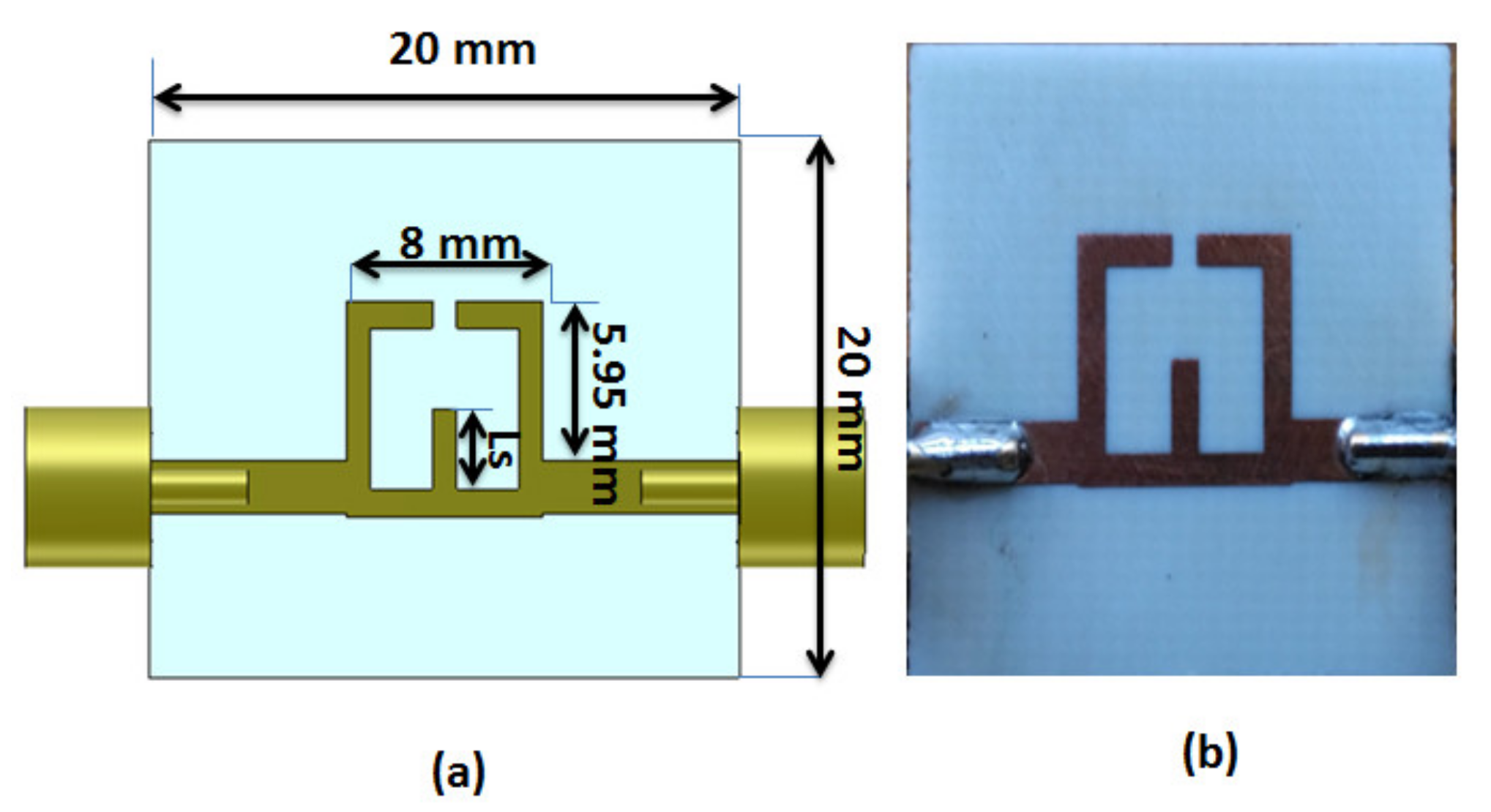
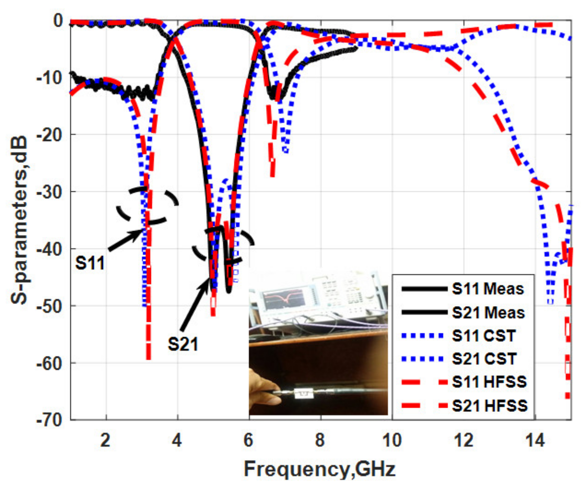
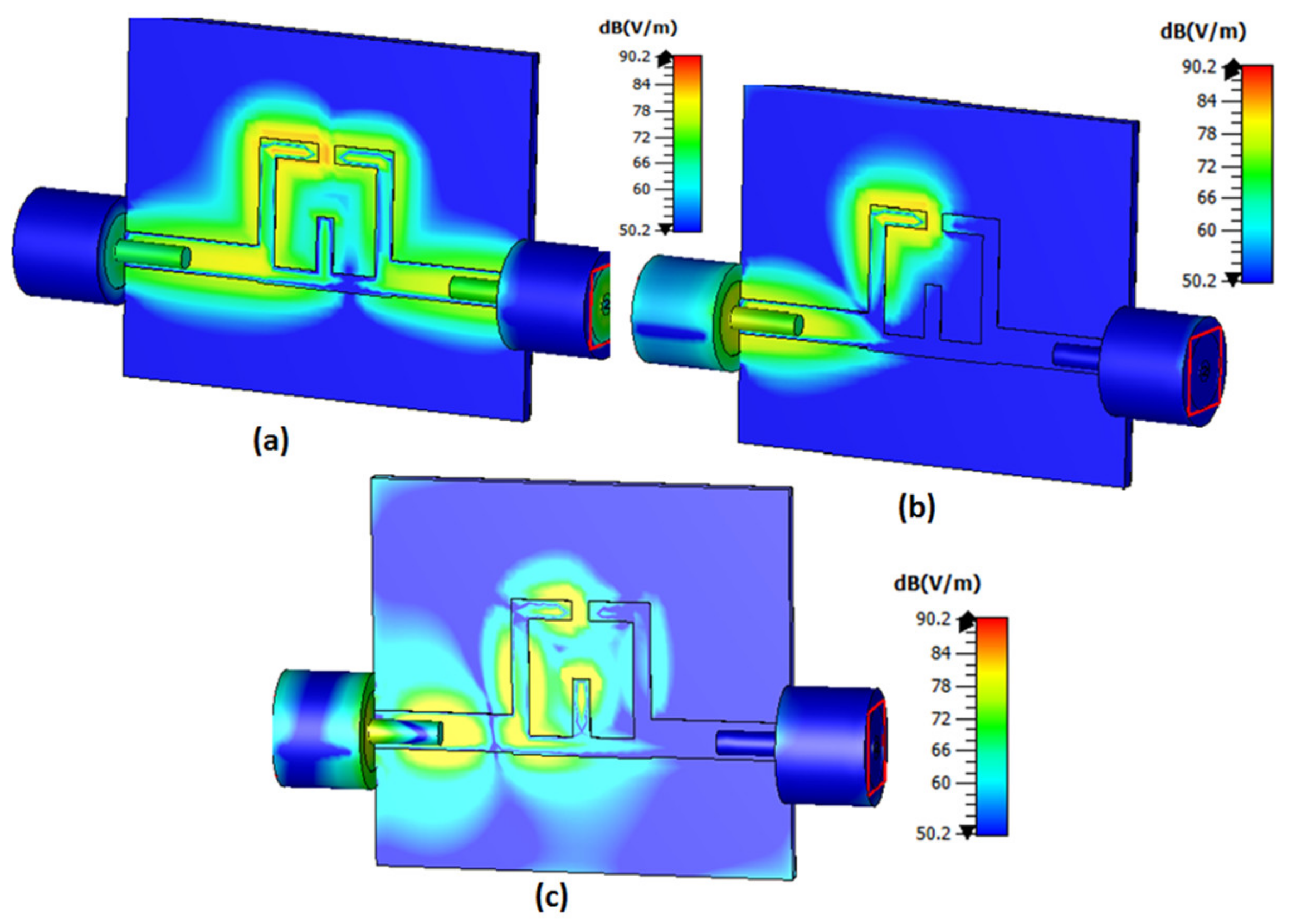
The 2-D structure of the open-loop resonator (OLR) band stop filter (BSF) loaded with stub is illustrated in Figure 1a. The BSF has open-loop transmission line structure with λ/2 length and loaded with the open-ended stub. The BSF OLR is fed by a 50 Ω microstrip line connected with SMA connectors. The RO4003 material with εr = 3.38, tan δ = 0.0027 and height = 0.813 mm is utilized as the designed filter substrate. The OLR BSF is fabricated as shown in Figure 1b and measured using vector network analyzer (VNA) HP19NE to validate its performance. The simulated (CST & HFSS) and measured S-parameters results of the BSF is demonstrated in Figure 2. The simulated fundamental mode of the operation of BSF is worked at a central frequency of 5.5 GHz, 3 dB bandwidth (BW) of 2.8 GHz, and around 0.3 dB return loss is accomplished through the entire rejection band area. As well as, it is clear from Figure 2 that the second mode is achieved at center frequency around 14.5 GHz. From the measured results, it is seen that the BSF has a central frequency of 5.5 GHz, BW = 2.4 GHz and return loss of around 0.4 dB in the rejection band area. Finally, it is evident from Figure 2 that the BSF simulated and measured results have the same trend. The electric field distribution results of the BSF at the primary and second modes 5.5/14.5 GHz (band stop region) and at 2.5 GHz (pass-band region) are shown in Figure 3 to show the filter operation. It is noticed that at 2.5 GHz the electric field is transferred to port 2 as shown in Figure 3a. However, at 5.5 GHz as shown in Figure 3b, the electric field did not exceed port 1 and was centered at the gap of the OLR. Moreover, the field distribution simulated at 14.5 GHz is illustrated in Figure 3c with a nonuniform distribution between the two ports, which confirms that the electric field could not pass to port 2 and is centered on the loaded stub.

Figure 1.
OLR with stub (a) 2-D configuration with dimensions (b) The fabricated photograph.

Figure 2.
The simulated and measured S-parameters of OLR with a stub.

Figure 3.
The electric field results of OLR with stub (a) at 2.5 GHz (b) at 5.5 GHz (c) at 14.5 GHz.
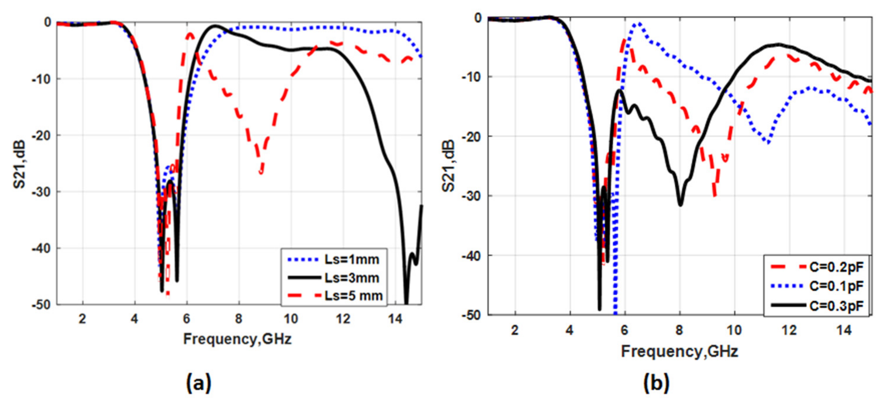
The parametric study is accomplished to investigate the effect of the stub lengths (Ls) and the lumped capacitors with capacitance (C) on the filter performance as shown in Figure 4. It is obvious from Figure 4a that the stub length (Ls) influences the resonance frequency of the second mode. The electric field distributions were centered on the stub at the second mode as shown in Figure 3c. So, by increasing the stub length (Ls), the inductance of the resonators increases, reducing the resonance frequency of the second mode as shown in Figure 4a. The resonance frequency was reduced to 14.5 GHz and 9 GHz when the Ls were increased to 3 mm and 5 mm, respectively. Also, we can claim from Figure 3c by incorporating the lumped capacitors at the region, which has the highest electric field, the capacitance of the resonator can be affected, and the frequency of the next mode can be tuned. As illustrated in Figure 4b, the resonance frequency can be reduced from 14.5 GHz (with no capacitor) to 11.5 GHz, 9.5 GHz and 8 GHz by utilizing a group of lumped capacitors with capacitance (C) of 0.1 pF, 0.2 pF and 0.3 pF, respectively.

Figure 4.
The insertion loss results of the OLR stub (a) at different values of the stub lengths (Ls) (b) at different values of lumped capacitors (C).
3. Second and Third-Order Filter Synthesis and Realization
This section presents the design and realization of second and third-order BPF with 180° feed structure depending on the optimization technique. The optimization technique is used to extract the required coupling matrix and external quality factor, which will achieve the desired filter specifications. First of all, our target here is minimizing the objective function in Equation (1) [26,27] to achieve the required coupling matrix and external quality factor.
The parameters ωzi′ and ωpi′ are the desired zeros and poles of (FN), FN can be calculated from Equation (2), where ω′ is the angular frequency which is variable and ωn′ is the nth transmission zero location. Finally, the value of the S11 and S21 can be calculated using equations in [26].
The values of R1 and R2 are the input and the output resistances, respectively, M is the coupling matrix and the identity matrix is U.
3.1. Second-Order BPF
In this section, we want to design the second-order band-pass filter with central frequency, return loss and BW of 3.5 GHz, 20 dB and 0.14 GHz, respectively, using the previous optimization technique. After the optimization technique is finished with the minimum value of the objective function (number of iterations = 17 and the algorithm is Quasi-Newton), the normalized coupling matrix (M) can be calculated as (7)
Also, the external quality factors equal q1 = q2 = 1.5. The denormalized (actual) coupling matrix = M × FBW.
Hence, the external quality factors equal q/FBW = 37.57.
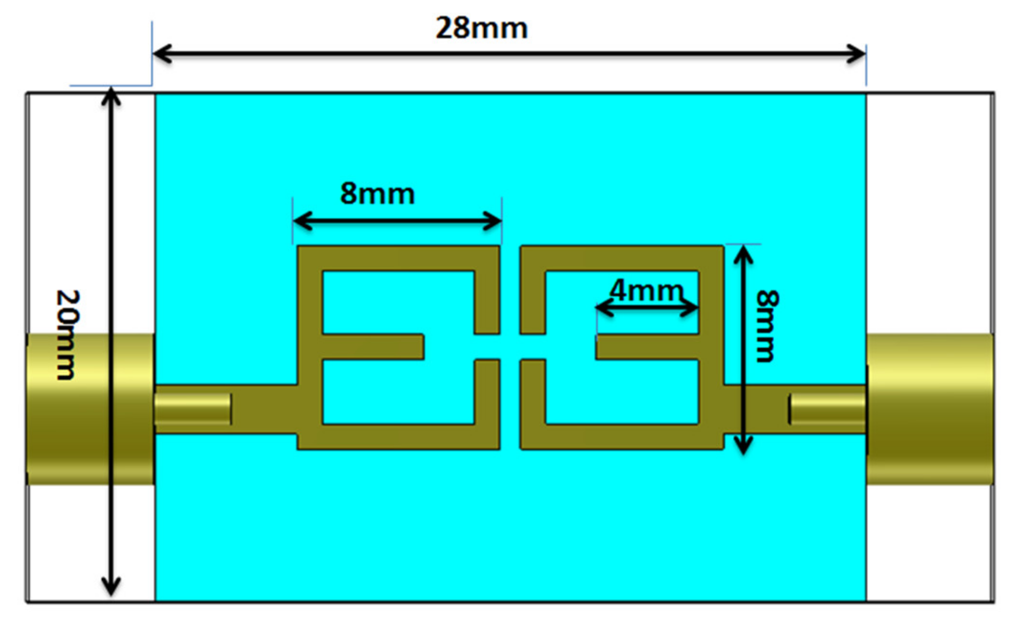
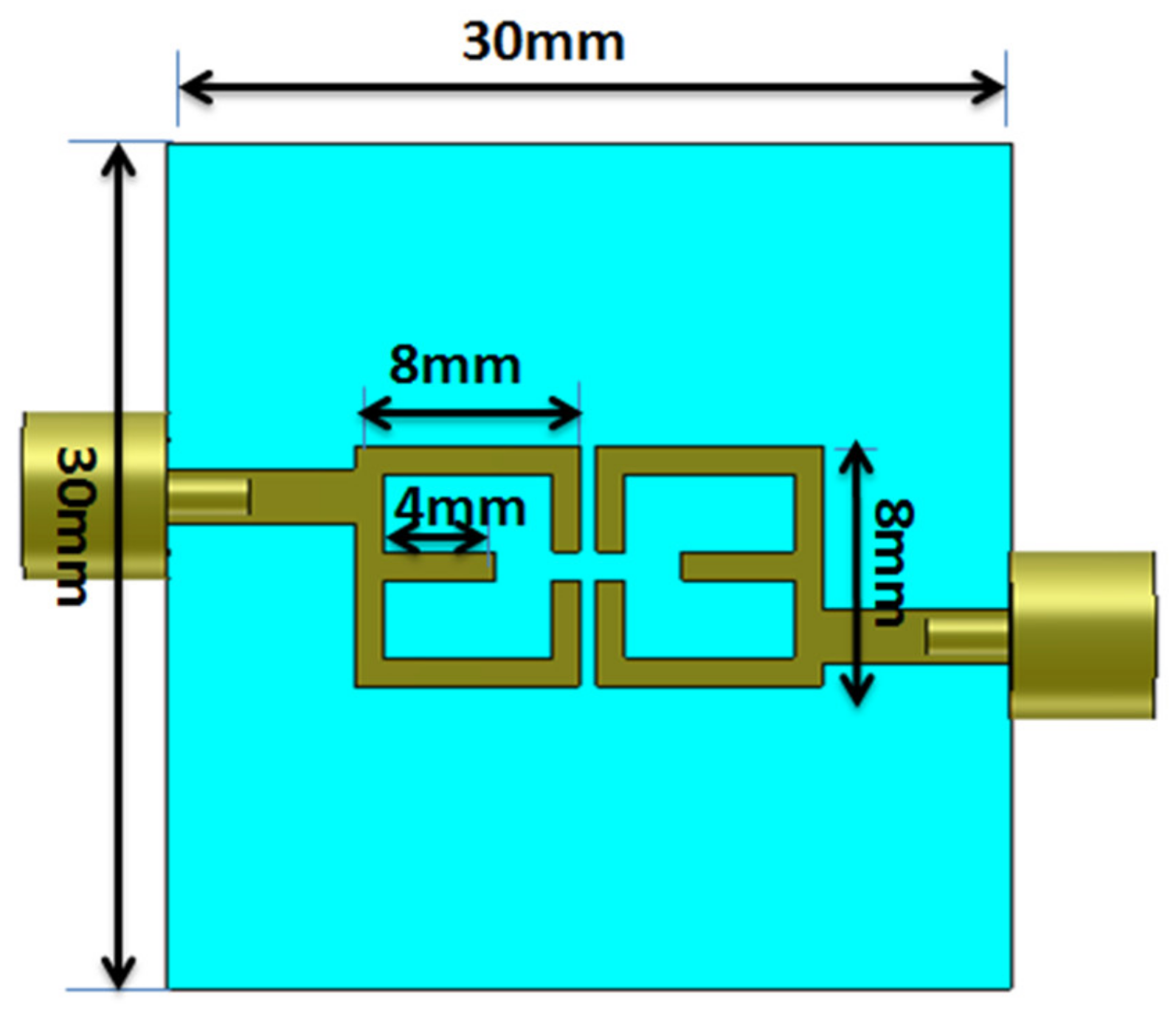
After the previous step of filter syntheses, the physical structure of the band-pass filter is determined using EM simulation depending on the values of coupling matrix and external quality factor. The filter configuration is shown in Figure 5; it shows that the filter is composed of two coupled resonators with half of a wavelength. The two resonators are open-loop resonators with small open stubs. The coefficients of coupling matrix can be approved by coupling the structure with 50 Ω microstrip feed weakly and the external quality factor can be validated by moving the feed line up and down the resonator.

Figure 5.
Second-order OLR with stub band-pass filter with 180° feed.
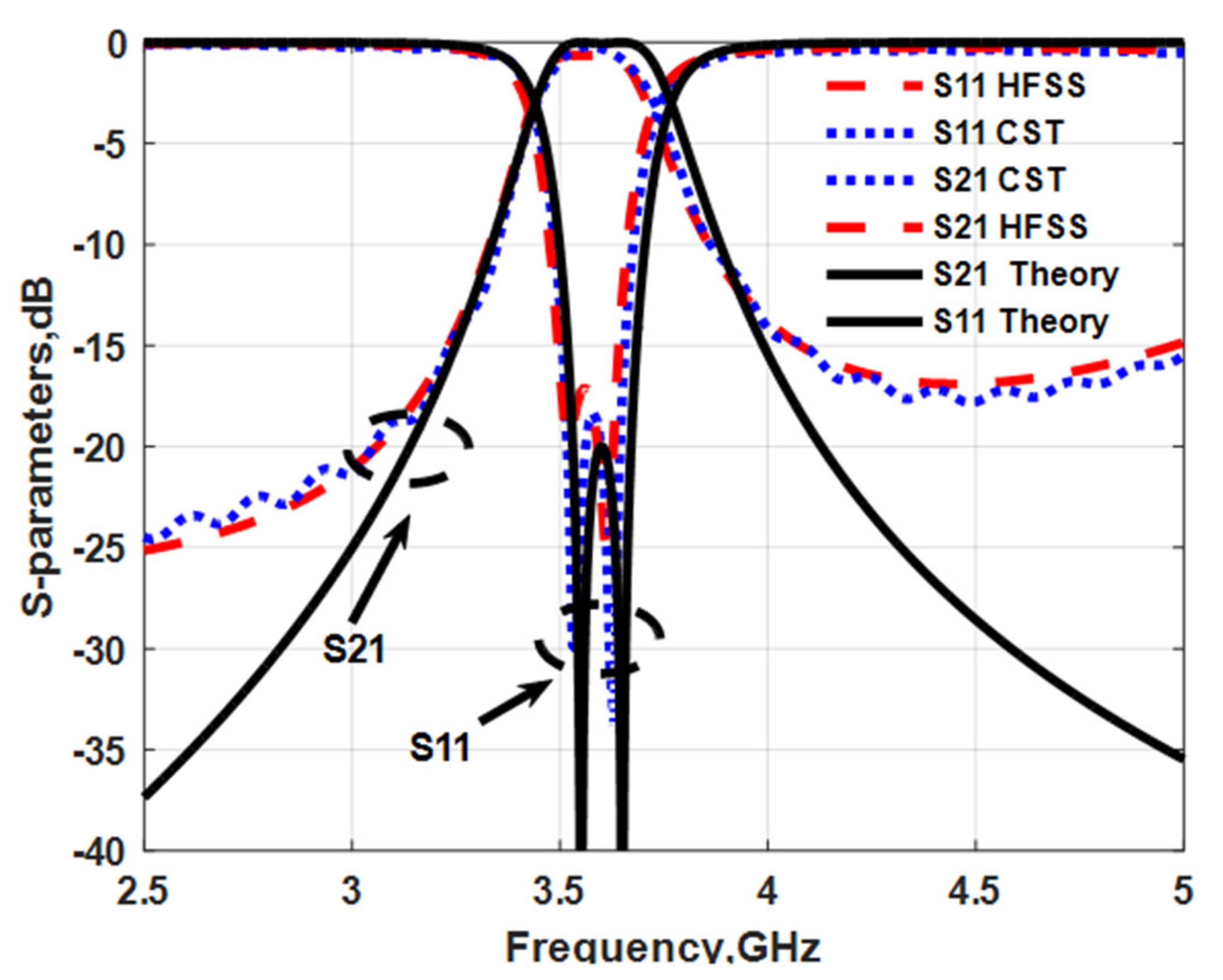
The filter is designed using R04003 substrate with εr = 3.38, h = 0.813 and tan δ = 0.0027. The CST and HFSS simulators are used in the filter design. The gap between the two resonators equals 0.6 mm and the distance of the feed line from the top to the resonator equals 0.8 mm to achieve the coupling matrix and external quality factor values. The simulated S11 and S21 results of the band pass filter using the optimization technique and the EM simulation (HFSS and CST) are shown in Figure 6. The filter is worked at fundamental mode at 3.5 GHz with 0.14 GHz bandwidth and around 20 dB return loss. Additionally, the theoretical results mimic the simulated data.

Figure 6.
S11, S21 simulated results of the second-order filter.
3.2. Third-Order BPF
This section introduces design of third-order BPF with central frequency, return loss, and BW of 3.5 GHz, 20 dB, and 0.22 GHz, respectively. A single transmission zero is chosen at 3.3 GHz before the center frequency using the previous optimization technique. Also, the position of the transmission zero can be chosen after the center frequency. After the optimization technique is finished with the minimum value of the objective function (number of iterations = 54 and the algorithm is Quasi-Newton), the normalized coupling matrix (M) can be calculated using (9)
Also, the external quality factors equal q1 = q2 = 1.17. The denormalized (actual) coupling matrix = M × FBW.
Consequently, the external quality factors equal q/FBW = 18.8.
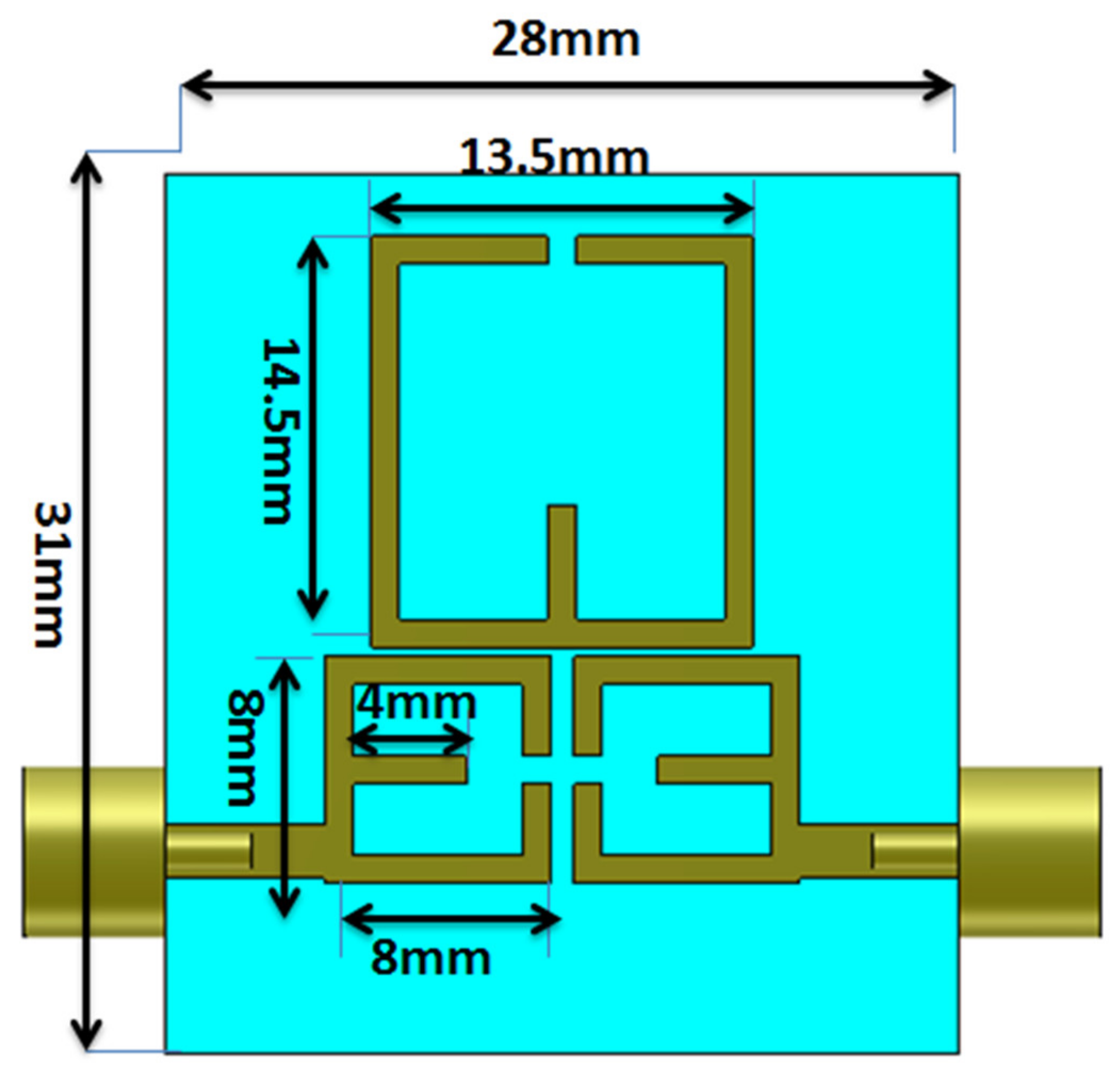
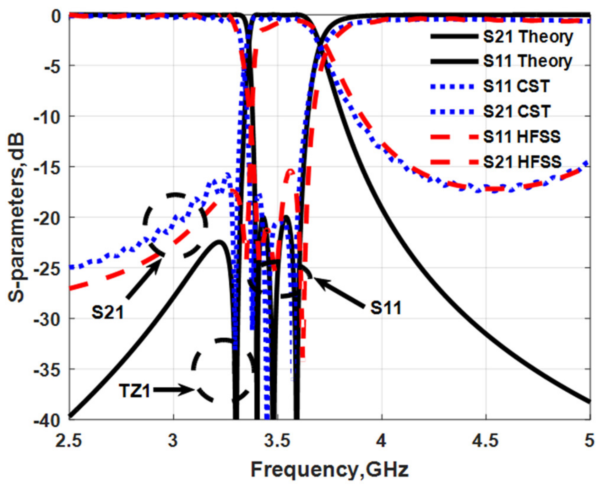
The physical structure of the third-order BPF is determined using EM simulation depending on the values of coupling matrix and external quality factor. The filter layout is shown in Figure 7; it shows that the filter is composed of two coupled resonators as previous second-order filter connected with the input/output ports and the third resonator is an open-loop resonator with larger size and coupled with the two resonators. The coefficients of coupling matrix can be approved by coupling the structure with 50 Ω microstrip feed weakly and the external quality factor can be validated by moving the feed line up and down the resonator. The filter is designed using the aforementioned substrate. The feed line’s distance from the top to the resonator equals 0.2 mm to achieve the external quality factor values. The simulated S-parameters (S11 and S21) results of the band-pass filter using the optimization technique and the EM simulation (HFSS and CST) are depicted in Figure 8. The filter is run at the fundamental mode at 3.5 GHz with 0.22 GHz bandwidth and around 20 dB return loss. The filter has a single transmission zero at 3.3 GHz to improve the filter selectivity at lower frequency bands. Furthermore, the theoretical results have good agreements with the simulated data.

Figure 7.
Third-order OLR with stub band-pass filter.

Figure 8.
S11, S21 simulated results of the third-order filter.
4. Feed Structure Dual-Band Pass Filter with Spiral Resonators
As shown in the previous section, the second and third-order filter are fed with feeding structure with 180°; hence, to improve the filter’s selectivity, the 0° feed structure is used as illustrated in Figure 9. The 0° feed structure introduces two transmission zeros without using extra resonator, which can be used to improve the filter performance and to reduce the filter size.

Figure 9.
2-D configuration of stub-loaded OLR BPF with 0° feed structure.
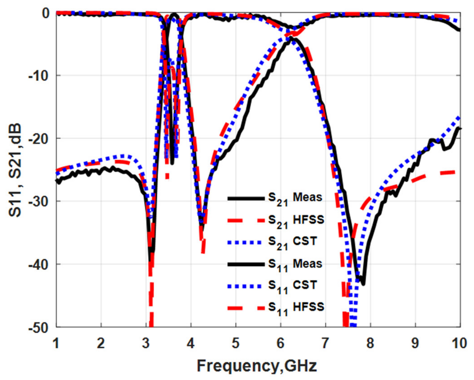
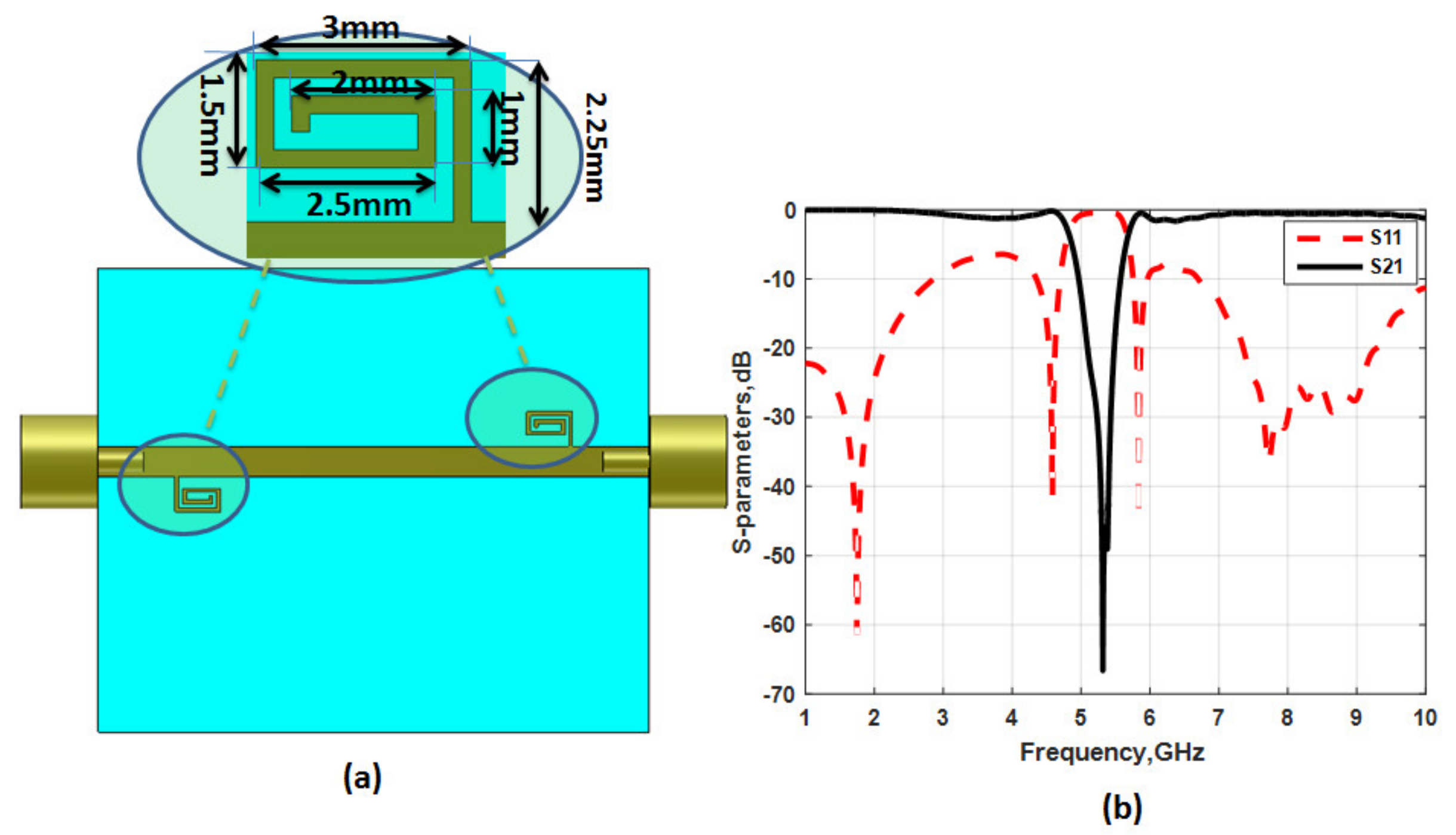
The 2-D configuration of the BPF is shown in Figure 9. The filter has the same dimensions as the previous second-order filter and is designed on the same substrate. The filter is feed with 0° feed structure (The input and output ports are aligned with the top and the bottom of the resonators, respectively). The simulated and measured results of S-parameters are illustrated in Figure 10, and it is seen that the filter is run at the center frequency of 3.5 GHz with 3 dB BW = 0.33 GHz, the insertion loss within the pass-band zone equals 0.7 dB; return loss equals −20 dB. The filter has two transmission zeros around the center frequency at 3.05 GHz and 4.25 GHz to enhance the filter selectivity and performance. There is a weak second band at 6 GHz due to the second mode as shown in Figure 10. In order to improve the performance of the second band, we introduced two ways. The first one is loading the microstrip line by two spirals resonators as shown in Figure 11a. The two resonators behave like a band stop filter, the dimensions of the two spiral resonators are optimized to operate around the second pass-band 6 GHz as shown in Figure 11. The BSF is designed to work at center frequency of 5.3 GHz and has pass-band zone at around 6 GHz as shown in Figure 11b. So, by combining the two resonators with the second-order filter shown in Figure 9, the second band at 6 GHz can be achieved and adjusted.

Figure 10.
S11, S21 simulated and measured results of stub loaded OLR with 0° feed BPF.

Figure 11.
Microstrip line loaded with spiral resonator band stop filter. (a) 2-D layout (b) S-parameters simulated results.
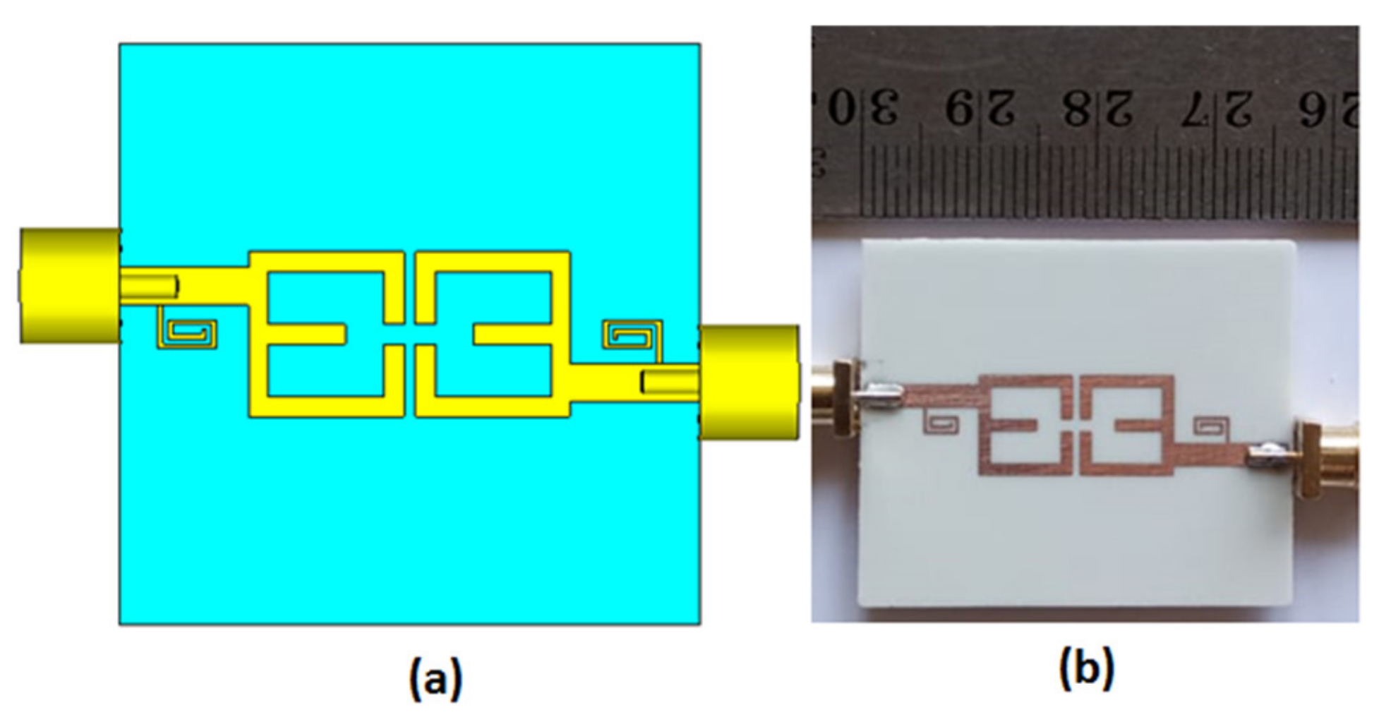
The 2-D structure of the proposed first second-order BPF loaded with two spiral resonators is shown in Figure 12a and the fabricated photo is illustrated in Figure 12b. The proposed filter is fabricated on the same substrate and measured using VNA to validate the simulated results, as shown in Figure 13.

Figure 12.
Stub loaded OLR with two spiral resonators BPF (a) 2-D layout (b) Fabricated photo.

Figure 13.
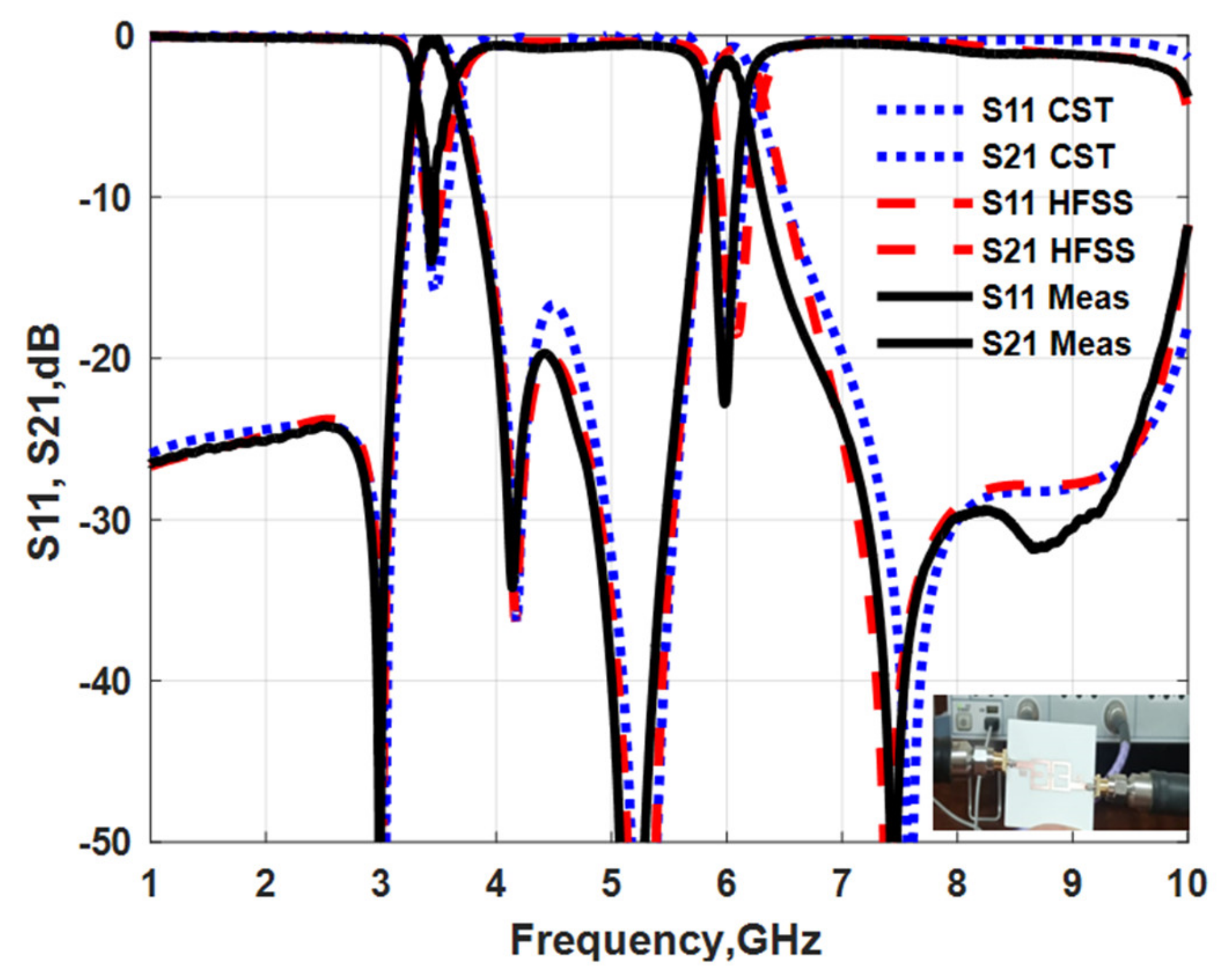
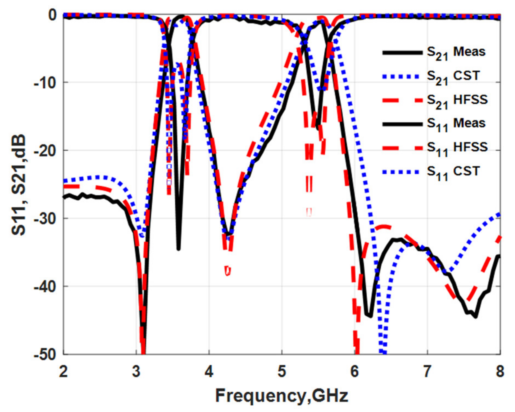
S11, S21 simulated and measured performance of dual-band stub loaded OLR BPF with 0° feed and two spiral resonators.
The measured results show that the proposed filter has two pass-band regions, the first band has central frequency of 3.5 GHz and the second band has central frequency of 6 GHz. The filter has 3 dB BWs of 0.33 GHz and 0.4 GHz, the pass-band insertion losses of 0.7 dB and 1.3 dB, and return losses in the pass-band of 14 dB and 20 dB, respectively. As well as, the proposed filter has 6 transmission zeros at 3.05 GHz, 4.25 GHz, 5.2 GHz, 5.38 GHz, 7.5 GHz and 9 GHz with more than 40 dB attenuation levels in the stop band zones to enhance the filter selectivity. Finally, the CST and HFSS simulated results are consistent with the measured results as demonstrated in Figure 13.
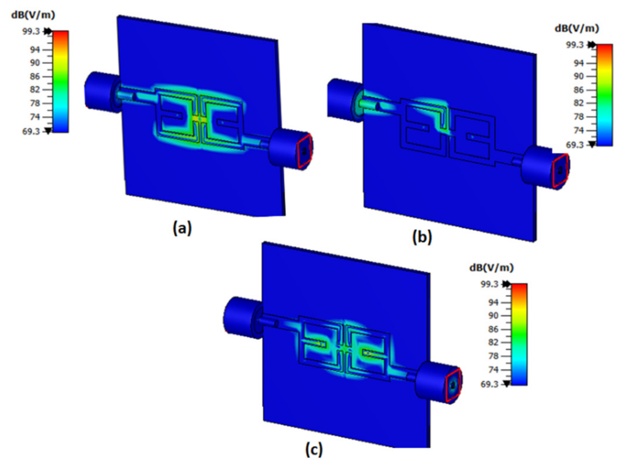
Figure 14 shows the electric field distribution results of OLR with 0° feed and two spiral resonators BPF at different frequency bands. At 3.5 GHz, the center frequency of the first pass-band zone, the electric field is exceeded from port 1 to port 2 as shown in Figure 14a. At the band stop region (5.3 GHz), the electric field is distributed around the spiral resonator and does not pass to the second port as shown in Figure 14b. Finally, at 6 GHz (the center frequency of the second band), the electric field is transferred to the second port as shown in Figure 14c.

Figure 14.
The electric field results of dual-band stub loaded OLR with 0° feed and two spiral resonators BPF. (a) at 3.5 GHz. (b) at 5.3 GHz. (c) at 6 GHz.
5. Feed Structure Dual-Band Dual Mode Band Pass Filter with Lumped Capacitors
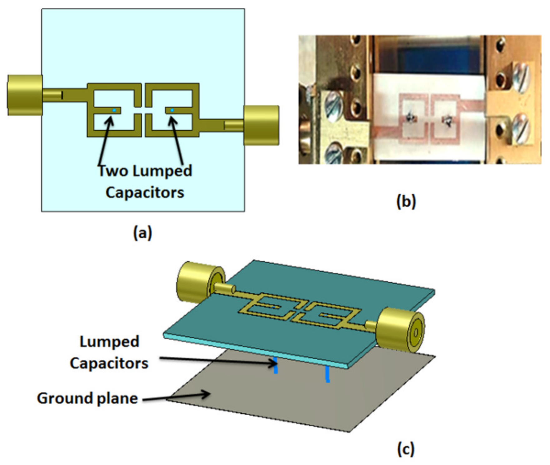
The second way to improve the second band’s performance is by loading the open-loop stub with two lumped capacitors as illustrated in Figure 15. As discussed in section two and shown in Figure 3, the field is collected around the open stub at the second harmonic (14.5 GHz), so by adding two capacitors as depicted in Figure 15 near the open end of the stub, the center frequency of the second harmonic can be changed and controlled.

Figure 15.
Second-order band-pass filter with 0° feed structure and two lumped capacitors. (a) 2-D configuration. (b) Fabricated photo. (c) 3-D configuration.
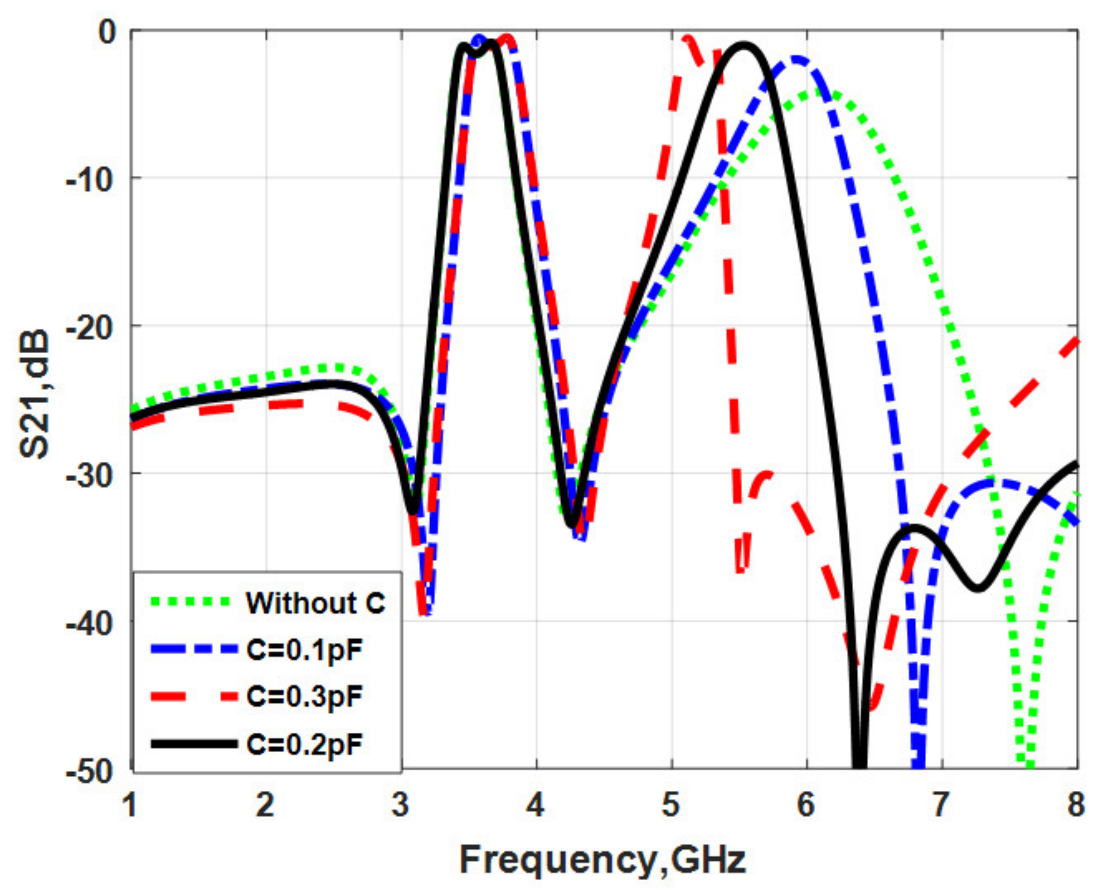
The S21 of the BPF with the varying of the lumped capacitors capacitance values is shown in Figure 16. The center frequency of the second harmonic mode is translated from 6.6 GHz (without capacitor) to 6, 5.5, and 5.3 GHz when lumped capacitors of 0.1 pF, 0.2 pF, 0.3 pF are embedded, respectively. However, the central frequency of the primary mode is fixed. The lumped capacitor increases the effective capacitance of the resonator so the resonance frequency can be decreased. Also, the lumped capacitor enhances the energy stored in the resonator which in turn increases the quality factor of the resonator at the expense of the bandwidth as shown in Figure 16 at C = 0.2 pF and 0.3 pF. As such, the tradeoff is utilized to achieve the best performance. At this point, band pass filter with dual-bands can be achieved. The filter is fabricated on the previous substrate with the same dimensions of the previous filter (16.6 × 8 × 0.813 mm3). Two surface mounted device (SMD) capacitors (CBR04C208A5GAC) with 0.2 pF are used in the fabrication process as shown in Figure 15. The lumped capacitor has the frequency range (1MHz–50 GHz) and has a size of 1 mm × 0.5 mm. The lumped capacitors are added vertically inside substrate through via holes and soldered from the top (open-loop stub) to the bottom (ground plane). The photograph of the experimentally fabricated BPF with two lumped capacitors is shown in Figure 15b.

Figure 16.
S21 of the BPF filter with various values of lumped capacitors.
The filter is tested using HP19NE (VNA) to validate the simulated results. The results of S11 and S21 measured and simulated are presented in Figure 17. From the measured results in Figure 17, it is seen that the filter is a dual-band filter with a central frequency of 3.5 GHz and 5.5 GHz, the 3 dB BWs equal 0.33 GHz and 0.42 GHz, the pass-band insertion losses equal 0.7 dB and 1.1 dB and the return losses in the pass-band equal 20 dB and 13 dB, respectively. The filter has four transmission zeros to improve the filter performance and selectivity at 3.04 GHz, 4.2 GHz, 6.35 GHz and 7.6 GHz with more than 40 dB attenuation levels in the stop band region. The filter has out of band suppression more than 20 dB up to 9 GHz. Finally, from Figure 17 it is observed that the filter has measured results with the same trend of the simulated results with a small shift because of the fabrication tolerance process.

Figure 17.
Simulated and measured S11 and S21 of the dual-band dual-mode BPF filter.
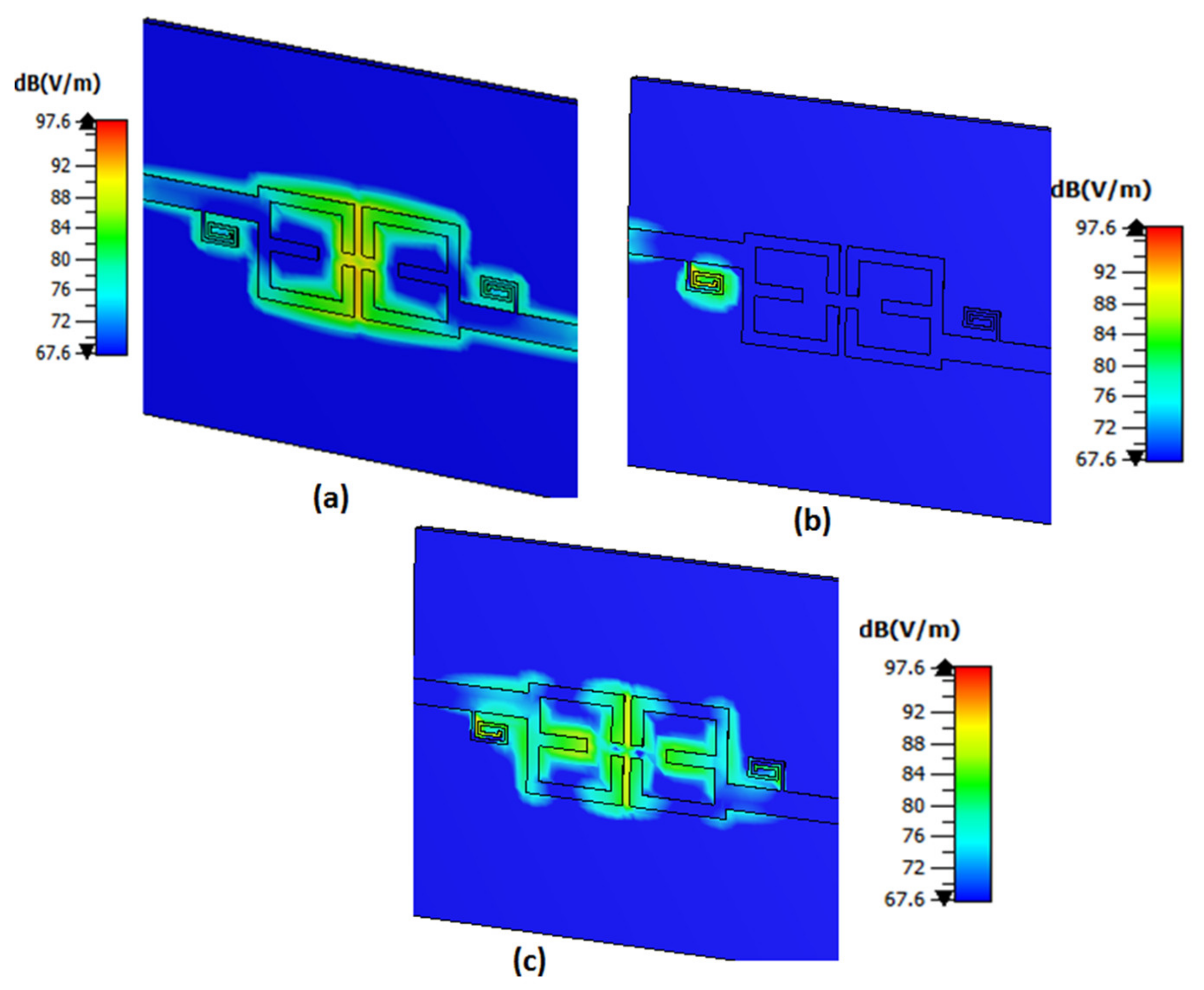
To understand the behavior of the proposed filter, the electric field distribution results at various frequency bands are studied as demonstrated in Figure 18. At 3.5 GHz (pass-band zone), the electric field is passed to port 2 as shown in Figure 18a. At 4.5 GHz (band stop zone), the electric field is distributed around the gap of OLR and does not pass to the second port as shown in Figure 18b. Finally, at 5.5 GHz (band pass zone), the electric field is transferred to the second port as shown in Figure 18c and the electric field is collected around the open-loop stub.

Figure 18.
The electric field results of dual-band dual mode with 0° feed BPF. (a) at 3.5 GHz. (b) at 4.5 GHz. (c) at 5.5 GHz.
Finally, Table 1 illustrates the comparison between our work and other works, which confirmed that the suggested filter has a simpler design, compact size and higher performance than others.

Table 1.
Comparison of the suggested models with the state of the art.
6. Conclusions
The design of dual-band dual-mode band-pass filter using coupling matrix technique has been presented. Two electrically coupled OLRs loaded with a stub using 0° feeding technique, two spiral resonators and lumped capacitors have been utilized to achieve the desired 3.5/5.5 GHz and 3.5/6 GHz frequency band to serve in wireless applications, especially WiMAX/WLAN applications. The first filter was designed to achieve fixed bands at 3.5/6 GHz, and the second filter has achieved fixed first band at 3.5 GHz, as well as the controlled band (second band at 5.5 GHz). The second band was achieved by exciting the second mode using lumped capacitors to operate at lower frequency band. The two designed filters have been fabricated and tested with good agreements with the simulated results. The filters have the advantages of small size, low insertion loss and good selectivity characteristics.
Author Contributions
Investigation, A.A.I.; Methodology, A.A.I. and W.A.E.A.; Software, A.A.I. and W.A.E.A.; Validation, M.A.A.; Writing—original draft, A.A.I.; Writing—review & editing, W.A.E.A. and M.A.A. All authors have read and agreed to the published version of the manuscript.
Funding
This research received no external funding.
Conflicts of Interest
The authors declare no conflict of interest.
References
- Ibrahim, A.A.; Abdalla, M.A.; Budimir, D. Coupled CRLH transmission lines for compact and high selective bandpass filters. Microw. Opt. Technol. Lett. 2017, 59, 1248–1251. [Google Scholar] [CrossRef]
- Hong, J.S.G.; Lancaster, M.J. Microstrip Filters for RF/Microwave Applications; Wiley: New York, NY, USA, 2001. [Google Scholar]
- Boutejdar, A.; Ellatif, W.A.; Ibrahim, A.A.; Challal, M. A simple transformation from lowpass to bandpass filter using a new quasi-arrow head defected ground structure resonator and gap-J-inverter. Microw. Opt. Technol. Lett. 2016, 58, 947–953. [Google Scholar] [CrossRef]
- Ibrahim, A.A.; Abdalla, M.A.; Ali, W.A. Small Size and Wide-Band Band Pass Filter with DGS/CRLH Structures. Appl. Comput. Electromagn. Soc. J. 2018, 34, 777–783. [Google Scholar]
- Deng, P.-H.; Tsai, J.-T. Design of Microstrip Cross-Coupled Bandpass Filter with Multiple Independent Designable Transmission Zeros Using Branch-Line Resonators. IEEE Microw. Wirel. Compon. Lett. 2013, 23, 249–251. [Google Scholar] [CrossRef]
- Rahman, M.U.; Ko, D.-S.; Park, J.-D. A compact tri-band bandpass filter utilizing double mode resonator with 6 transmission zeros. Microw. Opt. Technol. Lett. 2018, 60, 1767–1771. [Google Scholar] [CrossRef]
- Wei, F.; Yue, H.J.; Zhang, X.H.; Shi, X. A balanced quad-band BPF with independently controllable frequencies and high selectivity. IEEE Access 2019, 7, 110316–110322. [Google Scholar] [CrossRef]
- Gómez-García, R.; Loeches-Sánchez, R.; Psychogiou, D.; Peroulis, D. Multi-Stub-Loaded Differential-Mode Planar Multiband Bandpass Filters. IEEE Trans. Circuits Syst. II Express Briefs 2018, 65, 271–275. [Google Scholar] [CrossRef]
- Rahman, M.; Park, J.-D. A Compact Tri-Band Bandpass Filter Using Two Stub-Loaded Dual Mode Resonators. Prog. Electromagn. Res. M 2018, 64, 201–209. [Google Scholar] [CrossRef]
- Boutejdar, A.; Ibrahim, A.A.; Ali, W.A.E. Design of compact size and tunable band pass filter for WLAN applications. Electron. Lett. 2016, 52, 1996–1997. [Google Scholar] [CrossRef]
- Challal, M.; Mermoul, A.; Hocine, K. High-Frequency Microstrip Dual-Band Bandpass Filter Fabricated using FR-4 Glass Epoxy Material. J. Phys. D Appl. Phys. 2017, 50, 495602. [Google Scholar] [CrossRef]
- Boutejdar, A.; Mohamed, N.E.; Ibrahim, A.A.; Abdalla, M.A. New compact dual band-pass filter using coupled double-ring resonators and DGS technique. Appl. Comput. Electromagn. Soc. J. 2016, 31, 132–137. [Google Scholar]
- Tao, K.; Li, B.; Tang, Y.; Wu, Q. Multi-layer tri-band frequency selective surface using stepped- and uniform-impedance resonators. Electron. Lett. 2016, 52, 583–585. [Google Scholar] [CrossRef]
- Avinash, K.G.; Srinivasa Rao, I. Compact dual-band bandpass filter based on dual-mode modified star shaped resonator. Microw. Opt. Technol. Lett. 2017, 59, 505–511. [Google Scholar] [CrossRef]
- Kim, C.; Hyeon Lee, T.; Shrestha, B.; Chul Son, K. Miniaturized dual-band bandpass filter based on stepped impedance resonators. Microw. Opt. Technol. Lett. 2017, 59, 1116–1119. [Google Scholar] [CrossRef]
- Sun, L.; Deng, H.; Xue, Y.; Zhu, J.; Xing, S. Compact-Balanced BPF and Filtering Crossover With Intrinsic Common-Mode Suppression Using Single-Layered SIW Cavity. IEEE Microw. Wirel. Compon. Lett. 2020, 30, 144–147. [Google Scholar] [CrossRef]
- Deng, H.-W.; Zhao, Y.-J.; He, Y.; Liu, H.; Wang, H.-L. High selectivity and CM suppression wideband balanced BPF. Microw. Opt. Technol. Lett. 2014, 56, 2993–2998. [Google Scholar] [CrossRef]
- Aliqab, K.; Hong, J. UWB Balanced BPF Using a Low-Cost LCP Bonded Multilayer PCB Technology. IEEE Trans. Microw. Theory Tech. 2019, 67, 1023–1029. [Google Scholar] [CrossRef]
- Sengupta, A.; Roychoudhury, S.; Das, S. Design of a Miniaturized Multilayer Tunable Super Wideband BPF. Prog. Electromagn. Res. C 2020, 99, 145–156. [Google Scholar] [CrossRef]
- Arif, R.E.; Muslim, M.A.; Pramono, S.H.; Hsu, C.; Horng, T.S. Multilayer quad-band BPF with controllable transmission zeros. In Proceedings of the 2017 IEEE Asia Pacific Microwave Conference (APMC), Kuala Lumpar, Malaysia, 13–16 November 2017; pp. 722–725. [Google Scholar]
- Huang, L.; Yuan, N. A Compact Wideband SIW Bandpass Filter with Wide Stopband and High Selectivity. Electronics 2019, 8, 440. [Google Scholar] [CrossRef]
- Kim, P.; Jeong, Y. Compact and Wide Stopband Substrate Integrated Waveguide Bandpass Filter Using Mixed Quarter- and One-Eighth Modes Cavities. IEEE Microw. Wirel. Compon. Lett. 2020, 30, 16–19. [Google Scholar] [CrossRef]
- Yang, Z.; You, B.; Luo, G. Dual−/tri-band bandpass filter using multimode rectangular SIW cavity. Microw. Opt. Technol. Lett. 2020, 62, 1098–1102. [Google Scholar] [CrossRef]
- Zhao, F.L.; Weng, M.H.; Tsai, C.Y.; Yang, R.Y.; Lai, H.Z.; Liu, S.K. A miniaturized high selectivity band-pass filter using a dual-mode patch resonator with two pairs of slots. Microw. Opt. Technol. Lett. 2020, 62, 1145–1151. [Google Scholar] [CrossRef]
- Karpuz, C.; Gorur, A.K.; Sahin, E. Dual-mode dual-band microstrip bandpass filter with controllable center frequency. Microw. Opt. Technol. Lett. 2015, 5, 639–642. [Google Scholar] [CrossRef]
- Amari, S. Synthesis of Cross-Coupled Resonator Filters Using an Analytical Gradient-Based Optimization Technique. IEEE Trans. Microw. Theory Tech. 2000, 48, 1559–1564. [Google Scholar] [CrossRef]
- Seyfert, F.; Billa, S. General synthesis techniques for coupled resonator networks. IEEE Microw. Mag. 2007, 8, 98–104. [Google Scholar] [CrossRef][Green Version]
Publisher’s Note: MDPI stays neutral with regard to jurisdictional claims in published maps and institutional affiliations. |
© 2020 by the authors. Licensee MDPI, Basel, Switzerland. This article is an open access article distributed under the terms and conditions of the Creative Commons Attribution (CC BY) license (http://creativecommons.org/licenses/by/4.0/).

