Article

A Design of a Dual-Band Bandpass Filter Based on Modal Analysis for Modern Communication Systems

by
Ali Lalbakhsh
1,
Seyed Morteza Alizadeh
2,*,
Amirhossein Ghaderi
3,
Alireza Golestanifar
3,
Bahare Mohamadzade
1,
Mohammad (Behdad) Jamshidi
4,5,
Kaushik Mandal
6 and
Wahab Mohyuddin
7
1
The School of Engineering, Macquarie University, Macquarie Park, NSW 2109, Australia
2
Engineering Institute of Technology, Melbourne, VIC 3000, Australia
3
Young Researchers and Elite Club, Kermanshah Branch, Islamic Azad University, Kermanshah 6718997551, Iran
4
Regional Innovation Centre for Electrical Engineering (RICE), University of West Bohemia in Pilsen, 301 00 Pilsen, Czech Republic
5
Department of Electromechanical Engineering and Power Electronics (KEV), University of West Bohemia in Pilsen, 301 00 Pilsen, Czech Republic
6
Institute of Radio Physics and Electronics, University of Calcutta, Kolkata 700009, West Bengal, India
7
Research Institute for Microwave and Millimeter-Wave Studies, National University of Sciences and Technology, Islamabad 44000, Pakistan
*
Author to whom correspondence should be addressed.
Electronics 2020, 9(11), 1770; https://doi.org/10.3390/electronics9111770
Submission received: 25 September 2020 / Revised: 21 October 2020 / Accepted: 23 October 2020 / Published: 26 October 2020
(This article belongs to the Section Microwave and Wireless Communications)

Abstract

:
A dual-band bandpass filter (BPF) composed of a coupling structure and a bent T-shaped resonator loaded by small L-shaped stubs is presented in this paper. The first band of the proposed BPF covers 4.6 to 10.6 GHz, showing 78.9% fractional bandwidth (FBW) at 7.6 GHz, and the second passband is cantered at 11.5 GHz with a FBW of 2.34%. The bent T-shaped resonator generates two transmission zeros (TZs) near the wide passband edges, which are used to tune the bandwidth of the first band, and the L-shaped stubs are used to create and control the narrow passband. The selectivity performance of the BPF is analyzed using the transfer function extracted from the lumped circuit model verified by a detailed even/odd mode analysis. The BPF presents a flat group delay (GD) of 0.45 ns and an insertion loss (IL) less than 0.6 dB in the wide passband and a 0.92 IL in the narrow passband. A prototype of the proposed BPF is fabricated and tested, showing very good agreement between the numerically predicted and measured results.

1. Introduction

The development of wide-band communications has increased the application of wide-band microwave filters. Diverse design techniques and geometries have been proposed to design wide-band bandpass filters (BPFs) over the last few years. A wide-band BPF using an interdigital feed line loaded by stepped-impedance stubs was realized in [1], where a good out-of-band rejection, with a passband insertion loss (IL) and group delay (GD) of 0.57 dB and 5.91 ns, respectively were reported. A simple configuration of wide-band BPF using high impedance feed lines coupled with a bent stub was proposed in [2]. In this approach, the out-of-band suppression is controlled by the physical features of the bent stub. Another structure of BPF using stepped-impedance resonators (SIRs) was designed in [3] to achieve a 3 ns GD. Two parallel lines loaded with short and open stubs were introduced in [4] to realize a high frequency-selectivity near the passband. A wide-band BPF comprised of coupled short stubs with high selectivity was discussed in [5] that provides a 63% fractional bandwidth (FBW) and 0.6 dB of IL within its passband. A coupled feed line and open-circuited stubs were applied in [6] for designing a BPF operating over 1.22 to 2.77 GHz, presenting 6 ns GD. In [7], a spiral resonator was adopted to realize a wide-band filter, where the low and high cut-off frequencies are synchronously set. Substrate integrated waveguide (SIW) technology has widely been utilized to develop BPFs because of the associated low cost and simple topology [8,9,10,11]. The SIW filters generally present a low return loss (RL) throughout their passbands [8,9]; however, the size of the circuit can be undesirable for some applications [10,11]. In applications where high-level immunity to noise is critical, BPF with differential configurations is used [12,13]. An interdigital structure coupled with bent rectangular stubs has been proposed for designing wide-band BPF [14]. In this approach, the interdigital structure is used to feed the SIRs. It needs to be pointed out that the application of SIRs is not limited to wide-band BPFs, and they have extensively been used in all types of microstrip filters [15,16,17]. A multi-functional response has been achieved for a BPF using a stub-loaded ring [18]; however, the filter’s stopband is relatively small. A modified BPF with T-shaped resonators was designed in [19] to achieve a flat GD throughout a wide passband; however, only the passband’s upper edge is tunable. In another approach, BPFs were formed using the spiral lines in [20] to provide a high return loss in the passband, while the physical dimensions are not optimum, resulting in large BPFs. A simple structure composed of a feed line and rectangular resonator was discussed in [21] to provide dual-band performance. To minimize the BPF dimensions, a bent feed line was loaded by traditional stubs [22]. In a different approach, artificial intelligence has recently been introduced in the microwave and electromagnetic community and used to design a wide-band BPF [23,24,25].
In this paper, a dual-band passband filter with a modified T-shaped resonator is designed to provide a flat GD throughout a wide passband of 78.9%, where a bent T-shaped resonator is introduced to realize a tunable passband. Additionally, the bent T-shaped resonator is loaded by small L-shaped stubs to generate a second passband in the upper stopband which can be used for fixed satellite applications.

2. BPF Design

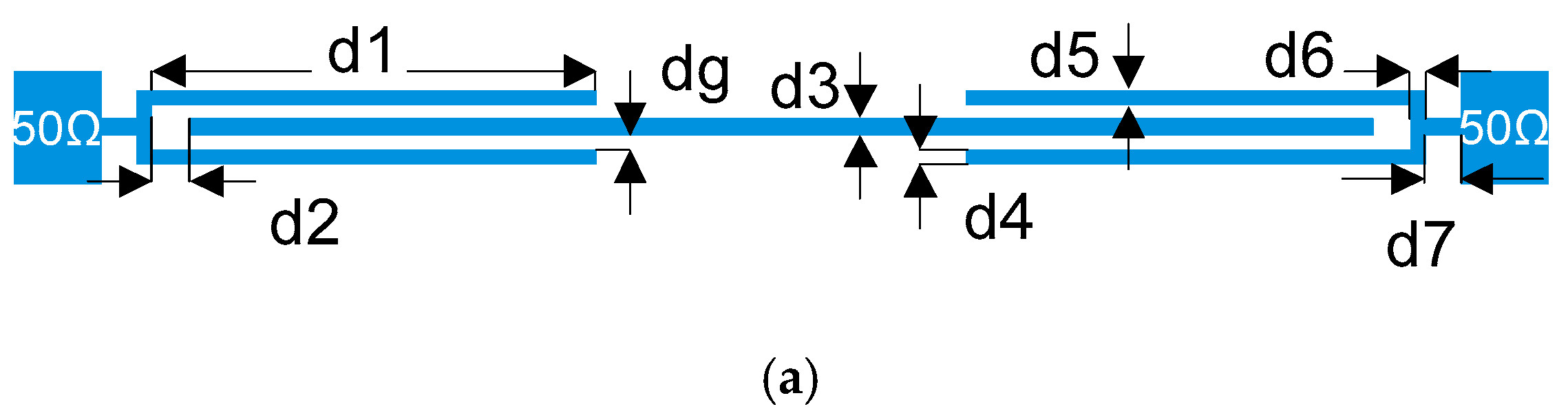
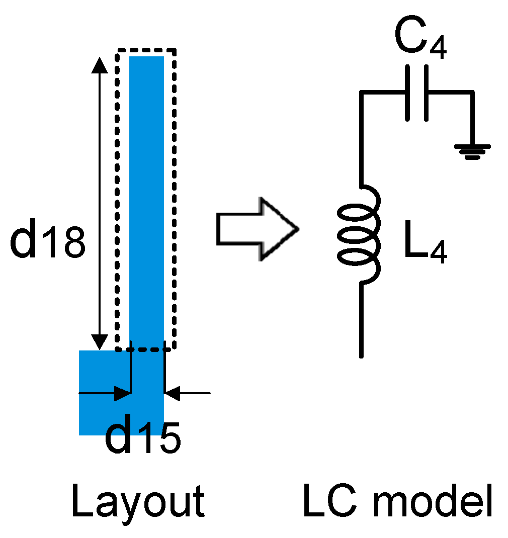
2.1. Coupling Structure

A wide-band coupling structure is designed using high impedance lines, as shown in Figure 1a. The electromagnetics simulation (EM) of the coupling system is carried out using the advanced design system (ADS) and shown in Figure 1b. According to this figure, the coupling system creates a wide passband from 5.5 up to 9.5 GHz; however, the transition bands are not sufficiently small, resulting in poor passband controllability.

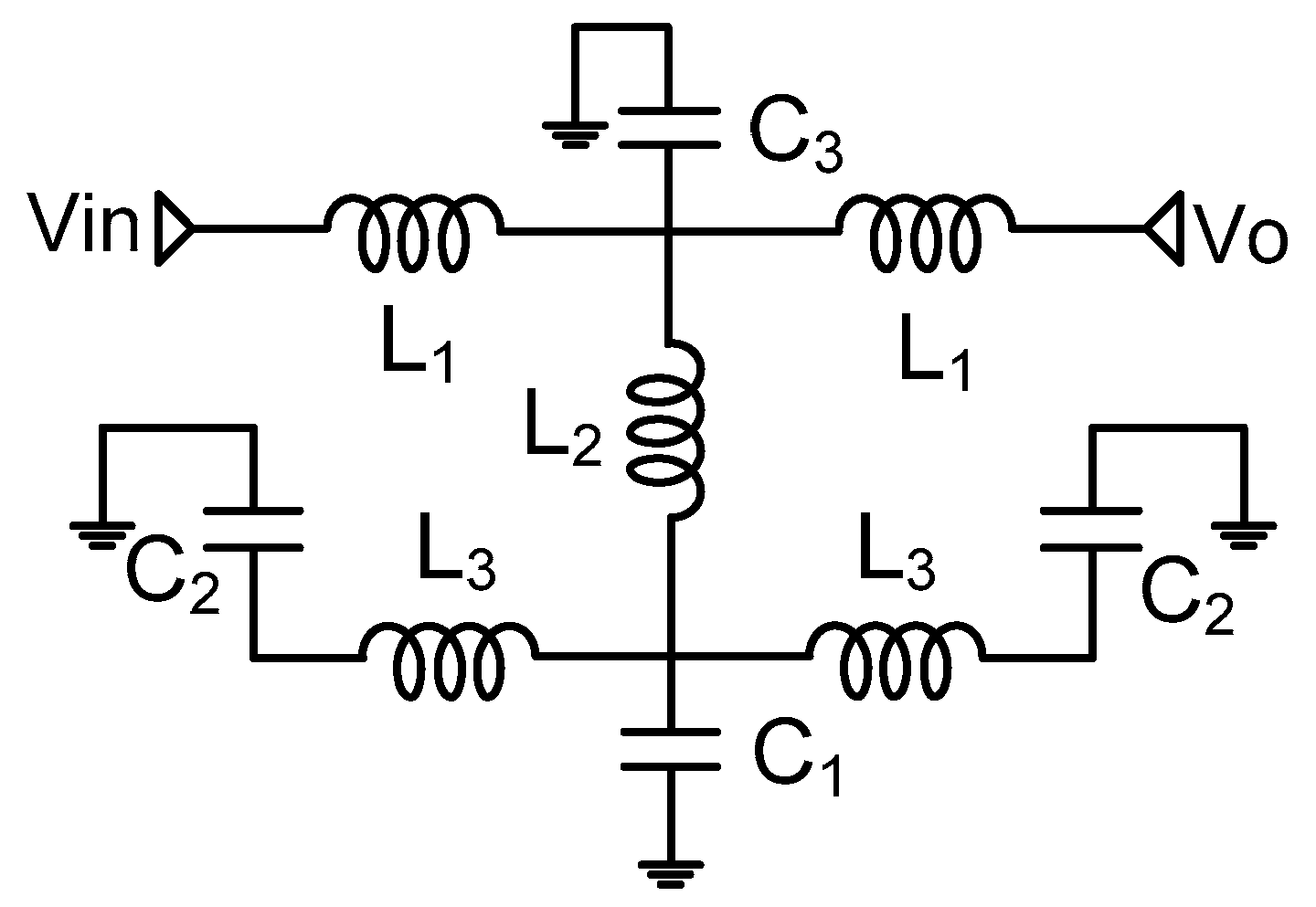
2.2. Single Wide-Band Response

To improve the sub-optimal filtering characteristics of the coupling structure mentioned above, a bent T-shaped resonator is added to the coupling structure, as depicted in Figure 2a. The S-parameters of the single-band BPF is presented in Figure 2b. As observed, the bent T-shaped resonator generates two TZs at 3.8 GHz (TZ1) and 11.6 GHz (TZ2). The passband bandwidth can be tuned by shifting the location of TZ1 and TZ2.
One of the reliable approaches to investigate the microstrip resonators’ frequency behavior is the use of lumped-element circuits (LCs) [26]. Here, a LC model is proposed for the bent T-shaped resonator and shown in Figure 3. In this model, L1 and C3 denote the high impedance feed line’s inductance and capacitance feed lines. L2 and C1 represent the inductance and capacitance of the low impedance line, respectively. C2 and L3, respectively, depict the capacitance and inductance of the bent stubs. It should be mentioned that the capacitance effects of the bent section are ignored in this model. Considering the model’s bent-related capacitance effects results in a more accurate model at a price of a significantly more complex model. The values of LC model parameters using the methods discussed in [26] are computed as follows: L1 = 5.8 nH, L2 = 1.931 nH, L3 = 2.01 nH, C1 = 0.446 pF, C2 = 0.198 pF, and C3 = 0.39 pF.
The bent T-shaped resonator’s transfer function is obtained from the LC model and shown in Equation (1), where r is the 50 Ω matching impedance. The equations of TZ1 and TZ2 are extracted from the transfer function and depicted in Equations (2) and (3). As observed, TZ1 and TZ2 are related to capacitors and inductors of the bent T-shaped resonator, including C2 and L3. Variations of C2 and L3 have a direct effect on the location of TZ1 and TZ2, which in turn controls the passband by shifting the low and high cut-off frequencies. Indeed, the upper edge of the passband can be tuned by varying L3 representing the inductance effects of length d11. Figure 4a,b depict the adjustability of the passband’s upper edge by varying d11 with a small effect on the lower edge of the passband. The lower edge of the passband can be adjusted by changing d12 corresponding to C2, as shown in Figure 4c,d.
V o V i n   =   2 r ( 1 + S 2 ( C 1 L 2 + 2 C 2 L 2 + C 2 L 3 ) + C 1 C 2 L 2 L 3 S 4 ) ( ( r + L 1 S ) ( r S ( C 1 + 2 C 2 + C 3 ) + S 2 ( C 1 ( L 1 + 2 L 2 ) + 2 C 2 ( L 1 + 2 L 2 ) + C 3 L 1 + 2 C 2 L 3 ) + r C 3 S 3 ( C 1 L 1 + C 1 L 2 + C 2 L 2 + C 2 L 3 ) + S 4 ( C 1 L 1 ( C 2 L 3 + C 3 L 2 ) + 2 C 1 L 2 C 2 L 3 + C 2 C 3 L 1 ( L 2 + L 3 ) ) + C 1 C 2 C 3 L 2 L 3 ( r S 5 + L 1 S 6 ) + 2 ) )
T Z 1   =   1 2 π C 1 L 2 + 2 C 2 L 2 + C 2 L 3 ( C 1 L 2 + 2 C 2 L 2 + C 2 L 3 ) 2 4 C 1 C 2 L 2 L 3 2 C 1 L 2 C 2 L 3
T Z 2   =   1 2 π C 1 L 2 + 2 C 2 L 2 + C 2 L 3 + ( C 1 L 2 + 2 C 2 L 2 + C 2 L 3 ) 2 4 C 1 C 2 L 2 L 3 2 C 1 L 2 C 2 L 3
The independent adjustability of the lower and upper edges of the passband can be investigated using the even/odd mode analysis, as explained in [27,28]. To compute the equations of the modal resonance frequency, the LC model of the bent T-shaped resonator is used, where the modal input impedances (Zine and Zino) are shown in Equations (4) and (5). In the resonance condition (Zine = Zino = 0), the Equations of even and odd mode resonance frequencies are approximately obtained by Equations (6)–(8). In this model, Cg denotes a weak coupling effect at input/output ports, and its value is 0.1 pF, approximately.
Z i n e = S C g ( 1 + S 2 C 2 L 3 + ( 2 S L 2 + S L 1 ) ( S C 2 + ( 1 + S 2 C 2 L 3 ) ( 2 S C 1 ) ) ) + S C 2 + ( 1 + S 2 C 2 L 3 ) ( 2 S C 1 ) S C g ( S C 2 + ( 1 + S 2 C 2 L 3 ) ( 2 S C 1 ) ) .
Z i n o = 1 + S 2 C g L 1 S C g .
f e 1 = 1 2 π 4 C 1 2 ( C 2 ( C 2 L 3 2 2 C g L 1 L 3 4 C g L 2 L 3 ) + C g 2 L 1 2 + 4 C g 2 L 1 L 2 + 4 C g 2 L 2 2 ) + 4 C 1 C 2 2 C g ( L 1 L 3 + 2 L 2 L 3 + L 3 2 ) + 4 C 1 C 2 C g 2 ( L 1 2 + 4 L 1 L 2 3 L 1 L 3 + 4 L 2 2 6 L 2 L 3 ) + C 2 2 C g 2 ( L 1 2 + 4 L 1 L 2 + 2 L 1 L 3 + 4 L 2 2 + 4 L 2 L 3 + L 3 2 ) + C g ( C 2 L 3 + 2 C 1 L 1 + 4 C 1 L 2 + C 2 L 1 + 2 C 2 L 2 ) 2 C 1 C 2 L 3 4 C 1 C 2 C g L 3 ( L 1 + 2 L 2 ) .
f e 2 = 1 2 π 4 C 1 2 ( C 2 ( C 2 L 3 2 2 C g L 1 L 3 4 C g L 2 L 3 ) + C g 2 L 1 2 + 4 C g 2 L 1 L 2 + 4 C g 2 L 2 2 ) + 4 C 1 C 2 2 C g ( L 1 L 3 + 2 L 2 L 3 + L 3 2 ) + 4 C 1 C 2 C g 2 ( L 1 2 + 4 L 1 L 2 3 L 1 L 3 + 4 L 2 2 6 L 2 L 3 ) + C 2 2 C g 2 ( L 1 2 + 4 L 1 L 2 + 2 L 1 L 3 + 4 L 2 2 + 4 L 2 L 3 + L 3 2 ) + C g ( C 2 L 3 + 2 C 1 L 1 + 4 C 1 L 2 + C 2 L 1 + 2 C 2 L 2 ) 2 C 1 C 2 L 3 4 C 1 C 2 C g L 3 ( L 1 + 2 L 2 ) .
f o = 1 2 π 1 C g L 1 .
To visualize the modal resonances and verify Equations (6)–(8), the bent T-shaped resonator is simulated under a weak coupling condition. Its S-parameters are plotted in Figure 5, where adjustability of the single-band BPF response is verified through the tunability of the modal resonances. It can be seen from Figure 5a,b that d11 mainly controls the higher even mode (fe2) with a small effect on the lower even mode (fe1), and d12 controls fe1, corresponding to the lower edges of the passband of the single-band BPF, as shown in Figure 4.
The proposed structure is formed using two small L-shaped stubs added to the bent T-shaped resonator for generating the second passband, as shown in Figure 6a. Figure 6b depicts the second passband fixed at 11.5 GHz.
The L-shaped stub and its LC model are presented in Figure 7, where the high impedance open stub is modeled by C4 and L4. The second passband can be tuned within a frequency window of 1270 MHz by varying L4 and C4 corresponding to the physical lengths of d18 and d15, respectively. Variations of the second passband versus d18 and d15 are shown in Figure 8. Another method to reshape the T-shaped resonator’s passband is using a slot in the T-shaped resonator, as explained in [29], where the current distribution of the T-shaped resonator is manipulated by removing a slot from the T-shaped resonator. This method is different from our method, as it can only introduce a narrow stopband within the initial passband. The introduction of the L-shaped stub in the presented approach creates a narrow passband outside the initial passband.
The advantage of introducing L-shaped resonators to the bent T-shaped resonator is the addition of a second controllable passband without affecting the filter’s total footprint. If such a narrow band is not required, the L-shaped resonators can be harmlessly removed from the filter configuration without affecting the primary passband performance.

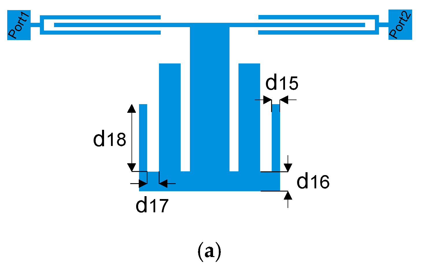
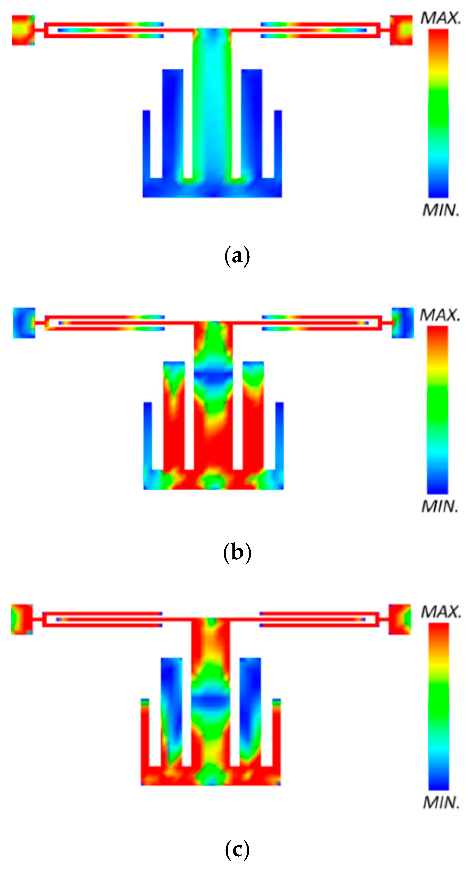
2.3. Current Distribution
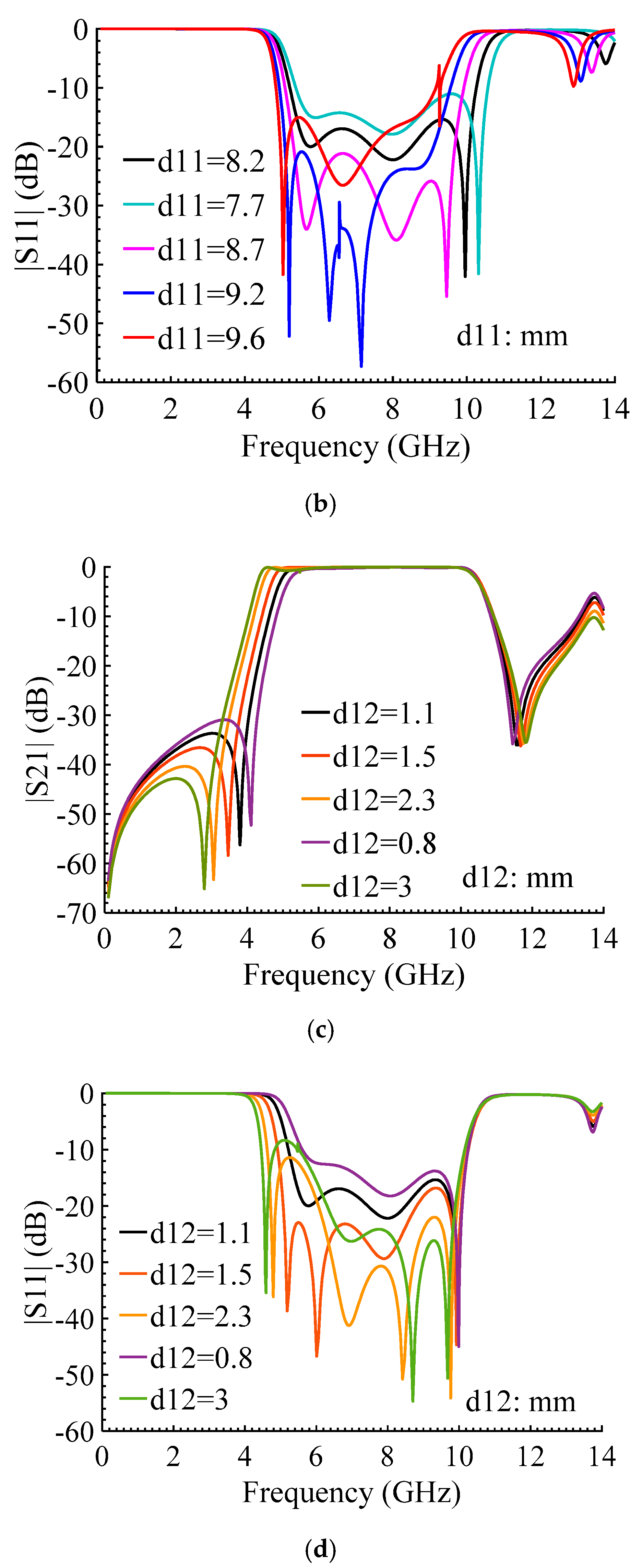
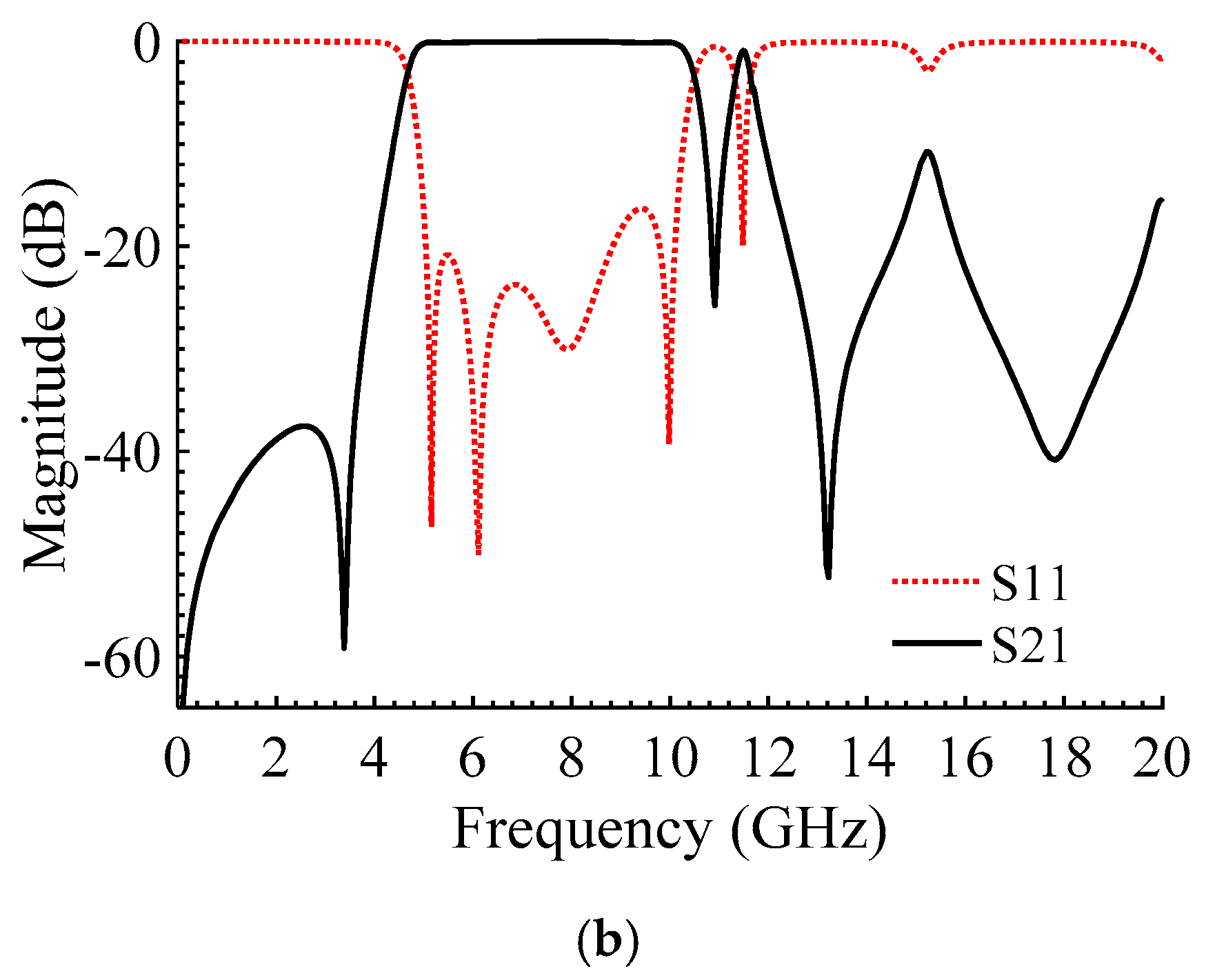
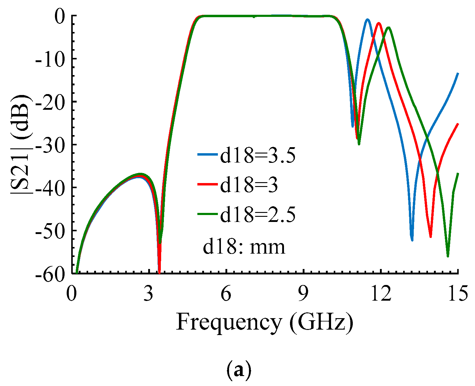
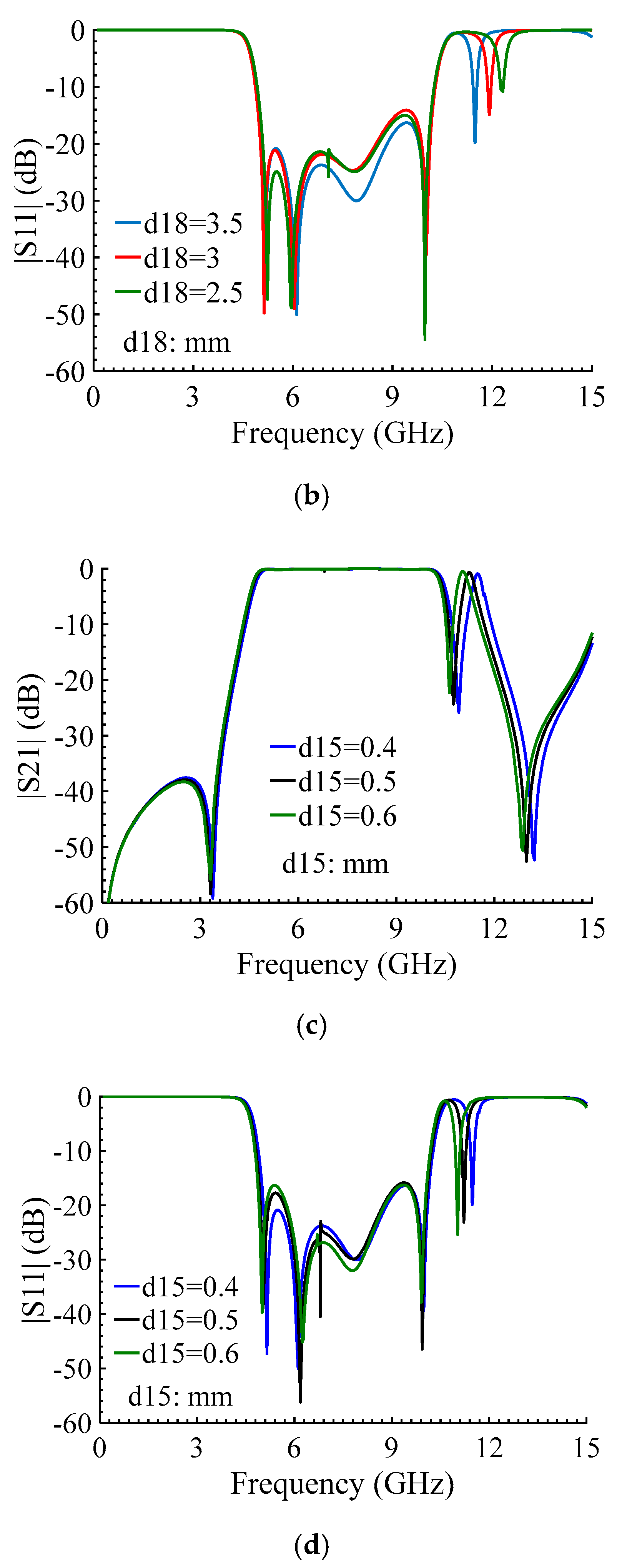
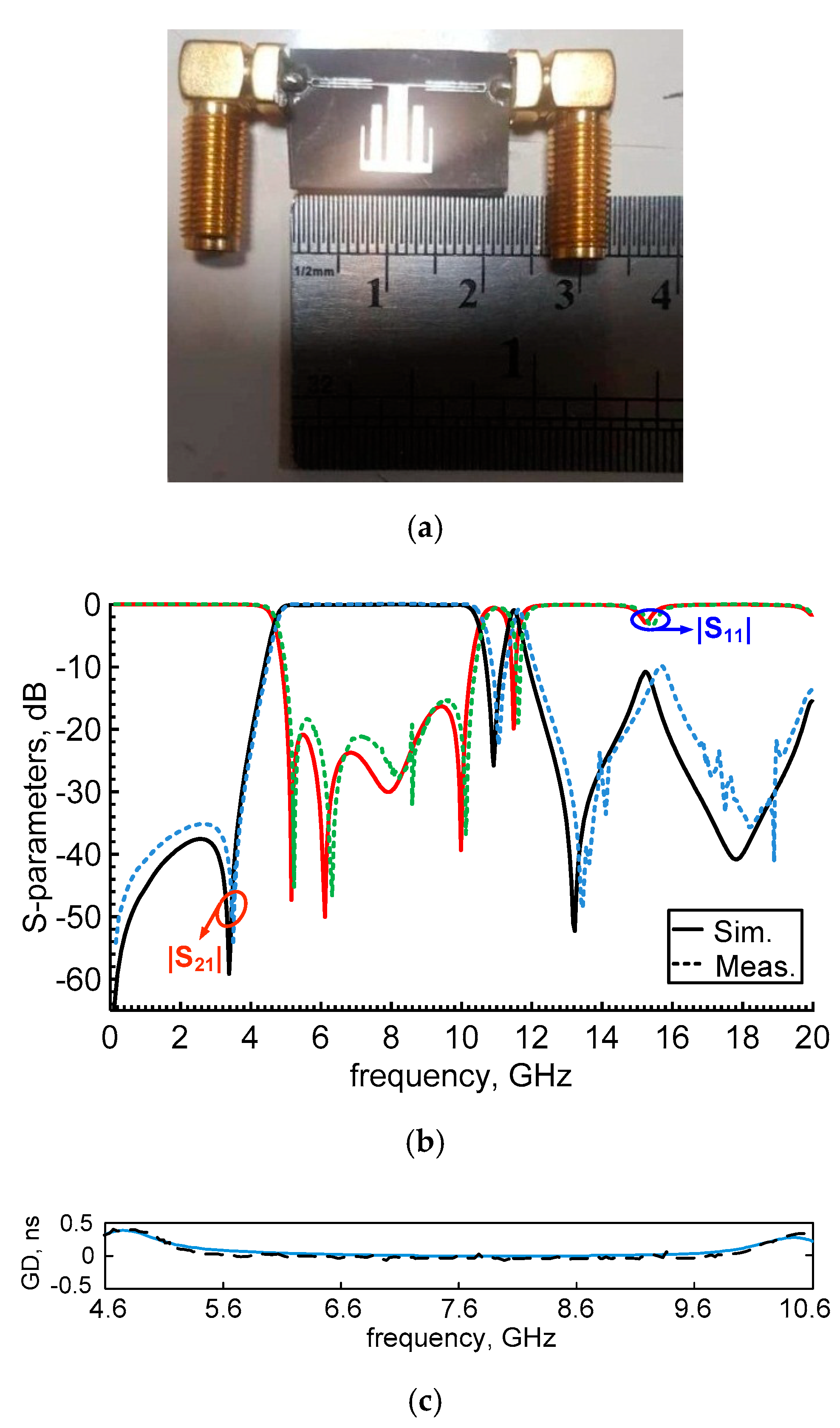
Current distributions are employed in this section to further investigate the effects of different filter sections on its frequency response. The current distributions are plotted at three typical frequencies in- and out-of-band response. As shown in Figure 9a, the bent T-shaped resonator and L-shaped stubs do not allow flowing strong currents at 1.76 GHz, representing the filter’s stopband. The current distributions are plotted at 9.68 and 11.5 GHz in Figure 9b,c, representing the filter’s wide and narrow bands, respectively. As seen, the bent T-shaped resonator at 9.68 GHz contributes to generating the wide passband, showing a strong current. The L-shaped stubs contribute most at 11.5 GHz to create the second passband, as shown in Figure 10c.

3. Results

A prototype of the proposed BPF was fabricated on a 5880 substrate with εr = 2.2, h = 0.508 mm, and loss-tangent of 0.0009, as depicted in Figure 10a. The filter measurement was carried out using an Agilent N5230A network analyzer. Experimental and simulation results are demonstrated in Figure 10b, showing very good agreement. The footprint of BPF is only 18.4 × 9 mm, corresponding to 0.64 × 0.31 λg, where λg is the guided wavelength at 7.6 GHz. The filter has a large FBW of 78.9%, extending from 4.6 to 10.6 GHz with a negligible IL of 0.136 dB (simulation) and 0.6 dB (measurement) and RL performance better than 16.32 dB. The second passband is fixed at 11.5 GHz with a bandwidth of 270 MHz from 11.35 to 11.62 GHz with 0.92 IL and 2.34% FBW for fixed satellite applications. The upper out-of-band rejection is better than 10 dB, extending up to 20 GHz and the lower stopband has a rejection level of 37 dB, from dc to 3.6 GHz. Figure 10c exhibits a flat GD of 0.45 ns throughout the large passband (4.6 to 10.6 GHz). The filter demonstrates a very good isolation level between the two passbands. According to the measurement results, an isolation level better that 22 dB has been achieved. Some of the important properties of recently published papers and the presented filter are classified and compared in Table 1.

4. Conclusions

A high-performance, dual-band BPF is proposed using double-coupled, high-impedance transmission lines and a bent T-shaped resonator loaded by L-shaped stubs. The former provides a large passband, and the latter improves the in-and-out band response of the filter. The filter’s performance is investigated using LC models and their extracted transfer functions are verified by EM simulations and measured results. The filter has a FBW of 78.9% centered at 7.6 GHz with a flat GD of 0.45 ns throughout the wide passband.

Author Contributions

Conceptualization, A.L., A.G. (Amirhossein Ghaderi), and A.G. (Alireza Golestanifar); methodology, A.L., A.G. (Amirhossein Ghaderi), and S.M.A.; software, A.L., A.G. (Amirhossein Ghaderi), K.M, and S.M.A.; validation, A.G. (Amirhossein Ghaderi), B.M., and A.G. (Alireza Golestanifar); formal analysis, A.L., M.J., K.M., and W.M.; resources, A.L. and S.M.A.; data curation, A.L. and A.G. (Amirhossein Ghaderi), M.J. and K.M.; writing—original draft, A.L., A.G. (Amirhossein Ghaderi), A.G. (Alireza Golestanifar), K.M and S.M.A.; writing—review and editing, all authors; supervision, A.L. and S.M.A. All authors have read and agreed to the published version of the manuscript.

Funding

This research received no external funding.

Conflicts of Interest

Declare conflicts of interest or state.

References

  1. Kumar, L.; Parihar, M.S. Quasi-Lumped Analysis of Wideband Bandpass Filter With High Out-of-Band Rejection Rate. IEEE Trans. Compon. Packag. Manuf. Technol. 2019, 9, 1549–1558. [Google Scholar] [CrossRef]
  2. Xu, K.-D.; Li, D.; Liu, Y. High-Selectivity Wideband Bandpass Filter Using Simple Coupled Lines With Multiple Transmission Poles and Zeros. IEEE Microw. Wirel. Compon. Lett. 2019, 29, 107–109. [Google Scholar] [CrossRef]
  3. Zakharov, A.; Litvintsev, S.; Ilchenko, M. Trisection Bandpass Filters With All Mixed Couplings. IEEE Microw. Wirel. Compon. Lett. 2019, 29, 592–594. [Google Scholar] [CrossRef]
  4. Xia, X.; Cheng, X.; Chen, F.; Deng, X. Compact UWB bandpass filter with sharp roll-off using APCL structure. Electron. Lett. 2018, 54, 837–839. [Google Scholar] [CrossRef]
  5. Zhang, T.; Bao, J.; Cai, Z.; Yang, Y.; Zhu, H.; Zhu, X.; Dutkiewicz, E. A C-Band Compact Wideband Bandpass Filter With High Selectivity and Improved Return Loss. IEEE Microw. Wirel. Compon. Lett. 2018, 28, 1–3. [Google Scholar] [CrossRef]
  6. Da Xu, K.; Zhang, F.; Liu, Y.; Nie, W. High selectivity seventh-order wideband bandpass filter using coupled lines and open/shorted stubs. Electron. Lett. 2018, 54, 223–225. [Google Scholar] [CrossRef]
  7. Lalbakhsh, A.; Karimi, G.; Sabaghi, F. Triple mode spiral wideband bandpass filter using symmetric dual-line coupling. Electron. Lett. 2017, 53, 795–797. [Google Scholar] [CrossRef]
  8. Chen, P.; Li, L.; Yang, K.; Chen, Q. Hybrid Spoof Surface Plasmon Polariton and Substrate Integrated Waveguide Broadband Bandpass Filter With Wide Out-of-Band Rejection. IEEE Microw. Wirel. Compon. Lett. 2018, 28, 984–986. [Google Scholar] [CrossRef]
  9. Pan, B.C.; Luo, G.Q.; Liao, Z.; Cai, J.L.; Cai, B.G. Wideband Miniaturized Design of Complementary Spoof Surface Plasmon Polaritons Waveguide Based on Interdigital Structures. Sci. Rep. 2020, 10, 3258. [Google Scholar] [CrossRef]
  10. Song, K.; Zhu, Y.; Zhang, F. Single- and dual-band filtering-response power dividers embedded SIW filter with improved output isolation. Sci. Rep. 2017, 7, 3361. [Google Scholar] [CrossRef] [Green Version]
  11. Zhao, C.; Fumeaux, C.; Lim, C.-C. Folded Substrate-Integrated Waveguide Band-Pass Post Filter. IEEE Microw. Wirel. Compon. Lett. 2016, 27, 22–24. [Google Scholar] [CrossRef]
  12. Dong, J.; Shi, J.; Xu, K. Compact Wideband Differential Bandpass Filter Using Coupled Microstrip Lines and Capacitors. IEEE Microw. Wirel. Compon. Lett. 2019, 29, 444–446. [Google Scholar] [CrossRef]
  13. Karimi, G.; Amirian, M.; Lalbakhsh, A.; Ranjbar, M. A new microstrip coupling system for realization of a differential dual-band bandpass filter. AEU Int. J. Electron. Commun. 2019, 99, 186–192. [Google Scholar] [CrossRef]
  14. Abdalla, M.; Choudhary, D.K.; Chaudhary, R.K. A compact reconfigurable bandpass/lowpass filter with independent transmission zeros based on generalized NRI metamaterial. Int. J. RF Microw. Comput. Eng. 2019, 30. [Google Scholar] [CrossRef]
  15. Dehghani, K.; Karimi, G.; Lalbakhsh, A.; Maki, S.V. Design of lowpass filter by using a novel Stepped Impedance Resonator. Electron. Lett. 2004, 50, 37–39. [Google Scholar] [CrossRef]
  16. Hosseinkhani, F.; Roshani, S. A compact branch-line coupler design using low-pass resonators and meandered lines open stubs. Turk. J. Electr. Eng. Comput. Sci. 2018, 26, 1164–1170. [Google Scholar]
  17. Karimi, G.; Siahkamari, H.; Hamedani, F.K.; Lalbakhsh, A. Design of Modified Z-Shaped and T-Shaped Microstrip Filter Based on Transfer Function Analysis. Wirel. Pers. Commun. 2015, 82, 2005–2016. [Google Scholar] [CrossRef]
  18. Jin, X.; Huang, X.; Chen, D.; Cheng, C. Response Diversity of Stub-Loaded Ring Bandpass Filter Based on Commensurate Line Element: Single- and Dual-Band Applications. IEEE Access 2019, 7, 25681–25689. [Google Scholar] [CrossRef]
  19. Liang, J.G.; Wang, C.; Kim, N.Y. Implementation of UWB BPF with modularised design based on SQR and DCR. IET Microw. Antennas Propag. 2018, 12, 1175–1184. [Google Scholar] [CrossRef]
  20. Luo, C.; Wong, S.-W.; Lin, J.-Y.; Yang, Y.; Li, Y.; Yu, X.-Z.; Feng, L.-P.; Tu, Z.-H.; Zhu, L. Quasi-Reflectionless Microstrip Bandpass Filters Using Bandstop Filter for Out-of-Band Improvement. IEEE Trans. Circuits Syst. II Express Briefs 2019, 67, 1849–1853. [Google Scholar] [CrossRef]
  21. Bi, X.-K.; Zhang, X.; Wong, S.-W.; Yuan, T.; Guo, S.-H. Design of Equal-Ripple Dual-Wideband Bandpass Filter With Minimum Design Parameters Based on Cross-Shaped Resonator. IEEE Trans. Circuits Syst. II Express Briefs 2019, 67, 1780–1784. [Google Scholar] [CrossRef]
  22. Liang, G.Z.; Chen, F.C. A Compact Dual-Wideband Bandpass Filter Based on Open-/Short-Circuited Stubs. IEEE Access 2020, 21, 20488–20492. [Google Scholar] [CrossRef]
  23. Yun, Y.-C.; Oh, S.-H.; Lee, J.-H.; Choi, K.; Chung, T.-K.; Kim, H.-S. Optimal Design of a Compact Filter for UWB Applications Using an Improved Particle Swarm Optimization. IEEE Trans. Magn. 2015, 52, 1–4. [Google Scholar] [CrossRef]
  24. Li, Y.S.; Wei, X.C.; Li, E.P. An asymmetric spiral-shaped DGS optimized by genetic algorithm for wideband common-mode suppression. In Proceedings of the 2015 Asia-Pacific Symposium on Electromagnetic Compatibility (APEMC), Taipei, Taiwan, 26–29 May 2015; pp. 681–684. [Google Scholar]
  25. Jamshidi, M.; Lalbakhsh, A.; Mohamadzade, B.; Siahkamari, H.; Mousavi, S.M.H. A novel neural-based approach for design of microstrip filters. AEU Int. J. Electron. Commun. 2019, 110, 152847. [Google Scholar] [CrossRef]
  26. Karimi, G.; Lalbakhsh, A.; Dehghani, K.; Siahkamari, H. Analysis of Novel Approach to Design of Ultra-wide Stopband Microstrip Low-Pass Filter Using Modified U-Shaped Resonator. ETRI J. 2015, 37, 945–950. [Google Scholar] [CrossRef]
  27. Weng, M.-H.; Lan, S.-W.; Chang, S.-J.; Yang, R. Design of Dual-Band Bandpass Filter With Simultaneous Narrow- and Wide-Bandwidth and a Wide Stopband. IEEE Access 2019, 7, 147694–147703. [Google Scholar] [CrossRef]
  28. Ahmadi, A.; Makki, S.V.; Lalbakhsh, A.; Majidifar, S. A novel dual-mode wideband band pass filter. Appl. Comput. Electromagn. Soc. J. 2014, 29, 735–742. [Google Scholar]
  29. Zhu, H.; Chu, Q.-X.; Tian, X.-K. Compact UWB bandpass filter using folded-T-shaped resonator with a notch-band. J. Electromagn. Waves Appl. 2012, 26, 1366–1373. [Google Scholar] [CrossRef]
Figure 1. Coupling structure: (a) Layout, dg = 0.1, d1 = 6, d2 = 0.5, d3 = d4 = d5 = d6 = 0.2, d7 = 0.5 (unit: Mm), (b) electromagnetics simulation (EM).
Electronics 09 01770 g001aElectronics 09 01770 g001b
Figure 2. Single-band bandpass filter (BPF): (a) Layout, d8 = 7, d9 = 7.5, d10 = 2, d11 = 8.2, d12 = 1.1, d13 = 1, d14 = 0.5 (unit: Mm), (b) EM simulation.
Electronics 09 01770 g002
Figure 3. Lumped-element circuit (LC) model for the bent T-shaped resonator.
Electronics 09 01770 g003
Figure 4. Passband tunability of the single-band BPF (Figure 2a): (a) |S21| variations versus d11, (b) |S11| variations versus d11, (c) |S21| variations versus d12, (d) |S11| variations versus d12.
Electronics 09 01770 g004aElectronics 09 01770 g004b
Figure 5. Tunability of the modal resonances of the bent T-shaped resonator: (a) Tunability of the higher even mode resonance using d11, (b) tunability of the lower even mode resonance using d12.
Electronics 09 01770 g005
Figure 6. Proposed BPF: (a) Layout, d15 = 0.4, d16 = 1, d17 = 0.6, d18 = 3.5 (unit: Mm), (b) EM simulation.
Electronics 09 01770 g006aElectronics 09 01770 g006b
Figure 7. L-shaped stub.
Electronics 09 01770 g007
Figure 8. Adjustability of the second passband: (a) |S21| variations versus d18, (b) |S11| variations versus d18, (c) |S21| variations versus d15, (d) |S11| variations versus d15.
Electronics 09 01770 g008aElectronics 09 01770 g008b
Figure 9. Current density distributions of the proposed BPF at different frequencies: (a) 1.76 GHz, (b) 9.68 GHz, (c) 11.5 GHz.
Electronics 09 01770 g009
Figure 10. Simulation and experimental results: (a) A photo of the fabricated prototype, (b) S-parameters, (c) group delay of the wide passband.
Electronics 09 01770 g010
Table 1. Specifications of cited papers and proposed one.
Refs.Passbands (GHz)BW (GHz)FBW (%)IL (dB)RL (dB)GD (ns) Size   ( λ g 2 )
[1]2.151.4–2.967.30.57135.910.080
[2]2.051.44–2.66600.62020.115
[3]2.051.96–2.084.961.512.23-
[4]6.853.1–10.6109.5-120.650.205
[5]5.13.5–6.7630.6220.60.095
[6]1.991.22–2.7778-1750.128
[7]7.84.8–10.8780.7120.40.220
[27]2.4/42.3–2.5/3-58/391.4/116/15-0.043
This work7.6/11.54.6–10.6/11.35–11.6278.9/2.340.6/0.9216.32/200.450.198
Publisher’s Note: MDPI stays neutral with regard to jurisdictional claims in published maps and institutional affiliations.

