Review

High-Voltage Temperature Humidity Bias Test (HV-THB): Overview of Current Test Methodologies and Reliability Performances

Department of Applied Science and Technology (DISAT), Polytechnic of Turin, 10129 Turin, Italy
*
Author to whom correspondence should be addressed.
Electronics 2020, 9(11), 1884; https://doi.org/10.3390/electronics9111884
Submission received: 7 October 2020 / Revised: 5 November 2020 / Accepted: 6 November 2020 / Published: 9 November 2020
(This article belongs to the Section Power Electronics)

Abstract

:
The high voltage temperature humidity bias test (HV-THB) has become increasingly popular for evaluating the performances of power semiconductor devices. Given the new challenges of the power semiconductor industry, several applications and devices need to be designed to withstand harsh environments during working operations, with a remarkable focus on high-humidity conditions. The HV-THB test allows one to activate and study different failure mechanisms which were not highlighted by the standard low voltage THB test, enabling new designs in several energy conversion fields, such as energy harvesting, industry and automotive applications. After a brief introduction of current test standards, this work goes through the current methodologies and state-of-the-art of the HV-THB test. The following sections are then dedicated to the knowledge about the failure mechanisms and the models for accelerated testing. Eventually, there is a section devoted to the main passivation materials in order to understand their effects on the HV-THB capabilities of the devices.

1. Introduction

The last few years have seen a remarkable drive toward the use of alternative energy sources, and the transition from fossil fuels to electric energy in several fields. For these reasons, the efficiency and reliability of power semiconductor applications have become critical focuses of the industry, along with the increasing of performances [1]. Therefore, researchers and designers in the field of power electronics are challenged to find new solutions and adapt current designs to achieve the expected transition into an electric world, while allowing all new technologies to meet and go beyond current safety and reliability requirements [2]. The only way to achieve this target is to intercept possible failures not only by following current regulations, but also going a step forward and testing devices and systems with increased stress, in order to broaden the spectrum of application for each piece of technology.
The presence of humidity is one of the most critical factors for the reliability of power semiconductor devices and circuits [3], and each component has its own sensitivity to this stressor, especially when high-voltage designs are considered [4,5], so that proper design rules must be implemented to avoid failure. Common power semiconductor devices are generally deployed in either plastic packages, where usually one or two devices are encapsulated in molding compound, or power modules, in which several power devices with a given topology are integrated into a single case filled with gel. In plastic packages, the penetration of moisture is very slow when compared to modules [6], since plastic packages offer a higher level of protection with respect to gel. That happens in the case of power module packages, easily allowing moisture penetration toward active areas of the devices [7].
When power devices are biased in humidity conditions, the co-presence of high-electric fields and moisture can trigger failure mechanisms which are different with respect to cases where each stressor is applied singularly, alongside with the temperature of the environment in which the device is operated. The high voltage temperature humidity bias (HV-THB) test is a device test which can be applied to power devices both in plastic packages and power modules [6,8,9,10]. In this kind of accelerated test, the devices undergo triple stress due to the simultaneous application of high-voltage reverse bias, high-humidity and temperature for a pre-determined period of time.
In this review, we will focus on HV-THB testing, comparing the methodologies, acceleration models, failure modes and passivation materials, in order to give an overview of state-of-the-art voltage-humidity testing for power semiconductor devices.

Current Normatives

As highlighted in the previous paragraph, the most tested vehicles are power modules and plastic packages. In the case of plastic packages, the current normative for discrete active electronic components is the AEC-Q101 [11] by the Automotive Electronics Council, entitled “Failure mechanism based stress test qualification for discrete semiconductors in automotive applications,” defining the minimum stress test requirements and conditions for automotive applications. This normative defines several tests in both static and dynamic environmental and electric conditions, including the humidity bias testing, named the high humidity high temperature reverse bias, or H3TRB. The test requires the devices to pass 1000 h test with an ambient temperature (Ta) of 85 °C and relative humidity (R.H.) of 85%, while reverse biased at 80% of rated blocking voltage (Vnom) up to a maximum of 100 V DC. Moreover, the devices must be electrically tested at least before and after H3TRB as a minimum requirement. In real qualification tests, devices under test (DUTs) are evaluated at defined times—for instance, 0 h, 168 h, 500 h and 1000 h—in order to record the evolutions of the electrical parameters in a more detailed way. It is important to notice that the current standard does not require continuous monitoring of any electrical parameters. In the case of power modules, the reference normative is the ECPE AQG 324, “Qualification of Power Modules for Use in Power Electronics Converter Units in Motor Vehicles” [12]; the H3TRB test is described in section QL-07. The static conditions of 85 °C and 85% R.H. are the same as those seen in AEC-Q101, while the maximum Vnom has a lower limit of 80 V. It should be noticed that this 80 ÷ 100 V limitation was set in order to satisfy the maximum temperature increase and maximum power dissipation required respectively by the IEC 60068-2-67 [13] and IEC 60749-5 [14], on which the latter regulations were based, in order to avoid unwanted self-heating that would drive away moisture [15] or the additional failure modes which are instead investigated by the HV-THB version of the test.
For both power modules and plastic packages, the DUTs must be electrically characterized before and after each test iteration until the 1000 h requirement is satisfied, and they need to be DC biased in blocking conditions for the whole duration of the test.
Table 1 shows a summary of the most important differences between current HV-THB parameters versus standard H3TRB, the details of which will be discussed in the following section.

2. Comparison of Test Methodologies

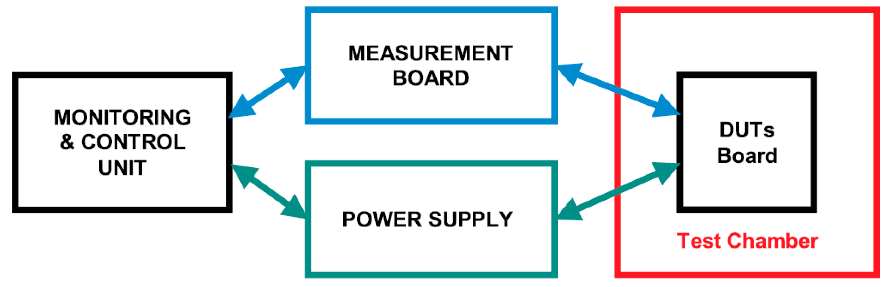
2.1. Test Setup and Procedures

Performing a high voltage test in high humidity conditions requires a dedicated setup, in most cases capable of continuous active monitoring of the DUTs [5,6,8,16,17,18], and with high voltage design rules requirements. A general schematic of the HV-THB test setup is shown in Figure 1 [8]. The DUTs are positioned on a high voltage biasing board or a dedicated rack inside a climatic chamber, allowing both environmental and electrical isolation with respect to the external environment. A high-voltage power supply unit (PSU) applies the voltage bias to the devices in the chamber and is controlled by a monitoring and control unit, usually a dedicated computer with ad hoc control software. Moreover, a measurement board with a dedicated active or passive circuit reads the leakage current values flowing through each device. Where possible, the control software can be also linked to the test chamber, in order to continuously monitor both humidity and temperature levels, which must be kept under control during the whole duration of the test. Moreover, an overcurrent limit is usually set to prevent extended damage in case of DUT failure [19], and active leakage monitoring can also be configured in order to remove device bias in cases of high leakage drift beyond a previously set value, so that critical failure is avoided and fine failure analysis can be carried out on the samples [8].
The testing procedure is generally performed as follows: the DUTs are tested with a curvetracer in order to obtain their reverse I-V characteristics, and are then positioned in the climatic chamber and integrated in the test circuitry. In order to avoid condensation, the chamber is ramped up to 85 °C and 85% R.H., and only after reaching stable conditions is the voltage applied. The devices are then monitored continuously, and the test is halted in order to perform intermediate reverse I–V characteristics to evaluate the status of the DUTs at desired checkpoints (0 h, 168 h, 500 h, etc.) up to their nominal blocking voltage Vnom or below their breakdown voltage (BV). At these checkpoints, the devices are left outside the testing chamber [6,8] or baked [20] in order to drive out moisture before testing at room temperature.

2.2. Leakage Current Monitoring

Leakage monitoring is a key feature when performing HV-THB, especially in the first hours of testing. In this period, the leakage curves usually show a peculiar transitory behavior that must be taken into account to properly set the test limits. This behavior is depicted in Figure 2. The leakage curve has an initial steep increasing trend, later evolving into an asymptotic decreasing behavior, which is probably caused by charge relocation inside the DUT and is not related to the typology of the device—for instance, there are metal oxide semiconductor field effect transistors (MOSFETs), insulated gate bipolar transistors (IGBTs), power diodes, etc. [7,8,9,19,21]. This behavior is always present, but no literature specifically addresses a model for this phenomenon.
In order to address this behavior, it is not possible to stick to the usual strategy of setting a rigid percentage limit to discriminate between test pass and fail. The general approach is to leave the DUTs to follow their evolutions, and after reaching the maxima of their respective curves, constantly read the minimum values of the curves and set those as the references for classical rigid limits in the form of:
I m o n i t o r e d <   α · I r e f e r e n c e ,
where α > 1 is a chosen positive constant defining the maximum limit with respect to the reference value [8,16]. It is important to notice that sometimes, during the asymptotic phase of the test, some devices could exhibit an unstable behavior (Figure 3). It can be seen that the DUTs overcome the fixed limit and subsequently go back to their asymptotic regime [10,16,22]. In this case, there is no clear agreement coming from the authors on whether to consider this behavior a pass or a fail, but its effect is something that needs to be considered when designing the final circuit.
A similar recovery behavior has been observed also during the HV-THB testing of SiC MOSFETs. In this case a DUT showed a temporary reduction in blocking voltage capability at 6000 h of testing, and later fully recovered its blocking voltage at the 9000 h checkpoint measurement [22].
Another point that should be examined regarding leakage current monitoring is the sampling time during the test. Considering the general evolution of a HV-THB monitoring curve, it is hard to define a standardized value for the sampling interval, which depends on the behavior of the technology under examination. For this reason, since a single sampling value cannot be defined, future standards will need to take this into account when defining the guidelines of the HV-THB testing in order to set a minimum monitoring frequency. For instance, authors report sampling rates ranging from 1 s [18] to 5 min [17].
Moreover, the presence of higher frequency peaks on the monitored signal [10] implies that the choice of a longer sampling time has to be considered only if the presence of these peaks is not meaningful with respect to the trend of the curve for the technology under examination, since these peaks could not be detected and averaged out by the longer sampling time. For this reason, it is also important to have stable temperature and humidity conditions inside the chamber, in order to remove secondary effects such as the periodic oscillation of the curves, which may be related to the thermostat and hygrostat cycle times inside the test chamber.

2.3. Intermediate Testing and Electrical Degradation

As already specified in Section 2.1, intermediate measurements are performed in order to evaluate device degradation at each checkpoint of the HV-THB testing. The observable degradation of characteristics generally occurs in two ways, as represented in Figure 4.
The first type of degradation is a decrease in breakdown voltage (Figure 4a), where the knee of the characteristic moves toward lower voltages, but without increasing the leakage values below the BV voltage. The second kind of degradation is the gradual increase of leakage on the whole characteristic (Figure 4b), but without significantly impacting the BV value. Both these electrical degradation mechanisms can happen at the same time, and have direct effects on the leakage current measured by the monitoring system.
It is important to highlight that the observable degradation of the characteristics, involving either an increase of leakage current or a decrease of BV, is mostly due to the wear out of passivation stacks in the junction termination regions, where voltage–humidity-related phenomena are generally localized [6,7,8,9]. These phenomena will be described in the following sections.

2.4. Accelerated Test Models

In order to define a model for the accelerated stress of the HV-THB, as proposed by several authors [7,9,17,20], it can be useful to list previously defined models in order to see which are the most suitable for the calculation of the acceleration factor.
First, we have the DiGiacomo model, a physical model developed to describe the behavior of metallic migration in encapsulated packages. This latter is defined in Equation (2) [23]:
t f = Q c β · J t i p
In this equation, tf is the time to failure for dendritic growth between the two biasing electrodes, Qc represents the critical amount of migrating metal ions required to achieve dendrite formation across the space between the electrodes, β is the degree of oxidation or fraction of active surface (which is metal dependent) and Jtip is the current density at the dendrite tip [24]. This model, which is based on Butler–Volmer’s equation relating electrode potential to current density [25], is indeed well defined from a physical point of view and gives good insights into the nature of the phenomenon, but it is not applicable to HV-THB testing because it needs to be related to the stressors of the test: temperature, humidity and voltage. For this reason, several models can be integrated in order to extrapolate the acceleration factor.
The first step is to consider the Arrhenius equation, linking temperature and reaction rate, described in Equation (3):
t f = A 1 · exp ( E A k · T )
where tf is the median time to failure, A1 is a fitting parameter, k is the Boltzmann’s constant, T is the absolute temperature and EA is the activation energy for the chemical reaction. The Arrhenius equation only considers the effect of temperature, so the model must be extended in order to include multiple stressors. A first approach to this extension could be achieved with the Eyring equation [24,26], but with the drawback of increasing the complexity of the equation.
For this reason, the Hornung model is preferred [27], and its equation was developed to describe dendritic growth based on the Arrhenius model [24] by adding the effect of voltage to the term A1 from Equation (3):
t f = α · d V · exp ( E A k · T )
In this equation, α is a fitting parameter, d represents the spacing between the electrodes and V is the applied voltage [24,27].
Furthermore, it is possible to consider the effect of humidity by considering Peck’s model [28]. This model extends the Arrhenius equation by including relative humidity to the Arrhenius model [28,29,30,31]:
t f = A 3 · R H x exp ( E A k · T )
where A3 and x are fitting coefficients, and RH is the relative humidity. In this way, by combining Hornung’s and Peck’s models (Equations (4) and (5)), it is possible to derive an acceleration factor for the stressors of the THB test [7,32,33,34]:
a f ( R H , T , V ) = ( R H a R H u ) x · exp ( E A k · [ 1 T u 1 T a ] ) · ( V a V u ) y
where the indices a and u refer respectively to the accelerated and usage conditions. However, this approach does not include the interaction between the stressors. For reference purposes, additional details regarding each model (Equations (2)–(6)) can be found in the work by Zorn et al. from 2014 [7].
Voltage can indeed be a strong acceleration factor; in fact, let us consider the example from [20]. Here a standard 80 V THB test is compared to a HV-THB test with a bias of 65% Vnom (780 V) applied to 1200 V IGBT module devices. In this case, the substitution of the latter values into Equation (6) gives an acceleration factor of 150, meaning that the standard 80 V value from AECQ101 applies a significantly lower amount of stress at fixed 85 °C/85% R.H. conditions. Moreover, due to the nature of the test, long runners make it hard to estimate the effective acceleration of the test and the validity of the model, especially at voltages below 60% Vnom. In order to overcome this issue and estimate the effect of acceleration, one option [7] is to measure the reduction of the breakdown voltage. For instance, as reported in Figure 5, it has been shown that by passing from a 65% to 90% Vnom reverse bias, the experiments show an acceleration factor of 2.1 [9], which is not a huge increase but significant for a test that can last for several thousands of hours.

3. An Overview of the Failure Modes

In Section 1, it was anticipated that different package technologies could behave differently with respect to humidity intake. For instance, it has been shown that power modules and small plastic packages (e.g., standard TO-247) have significantly different moisture uptakes. In fact, for a standard MTP power module, a weight increase of 1.9 g has been measured after 24 h at 85 °C/85% R.H, mostly absorbed by the silicon gel, while it is not possible to measure a significant change in weight for a TO-247 package exposed to the same conditions [6]. The presence of humidity together with the applied bias can activate a chain of chemical reactions, leading to corrosion and consequently device degradation and failure.

3.1. The Corrosion Cell

The corrosion process starts with the hydrolysis of water adsorbed by the surface between the biased electrodes, forming a so called “corrosion cell.” This happens on the anode’s surface, with the formation of hydrogen, according to the following oxidation reaction:
2   H 2 O   O 2 ( g ) + 4 H + + 4   e
Differently, the cathode side presents a reduction reaction with the formation of hydroxide ions and hydrogen gas [20,35,36,37,38]
2 H 2 O + 2 e H 2 ( g ) + 2 ( OH ) 2 H 2 O + O 2 + 4 e 4 ( OH )
In this way, the anode side process yields a locally acidic solution, and the cathode side a basic one. Thus, a pH gradient is formed between the electrodes.

3.2. Aluminum Corrosion

Aluminum is very reactive and Al(OH)3 forms at its surface when in presence of water, yielding a high oxidation resistance at pH values between 4 and 9 [39,40,41,42]. Outside this range, the aluminum hydroxide can react as an acid or a base depending on the properties of the solution (i.e., pH and equilibrium potential). In the case of an acid solution, Al(OH)3 is oxidized as follows:
Al ( OH ) 3 + 3 H   Al 3 + + 3 H 2 O
These ions are very unstable in solution, so the probability of them reaching the cathode by migration is very low. Oppositely, on the cathode side, the Al(OH)3 can form aluminates following the reaction:
A l ( OH ) 3 + OH [ Al ( OH ) 3 ]
Differently from Al3+ ions, these aluminates are very stable and can migrate in the solution, form a precipitate on the anode side or even form complex salt ions on their migration path.
In addition, an alternate source of gaseous H2 with respect to water hydrolysis can be the following:
Al + 3 H 2 O   Al ( OH ) 3 + 3 2 H 2
This gaseous hydrogen, and the product of Equation (8), can lead to blistering and delamination of the upper passivation layers [6,43]. The whole reaction is represented schematically in Figure 6 [9], where the process is described schematically in Figure 6a, while a real example of aluminum corrosion is shown in Figure 6b.

3.3. Electrochemical Migration (ECM)

Section 3.2 has shown how aluminum has a peculiar migration behavior when a corrosion cell is built, but not all metals have the same behavior with respect to transport under an electric field. For instance, for Cu and silver, which are common materials involved in powered device manufacturing, failure due to ECM can be observed since the native metal oxides of these materials can be easily decomposed, and due to local acid conditions, metal ions are produced by corrosion at the anode, following the reaction [20,44]:
M M n + + ne
The metal ions produced at the anode are then accelerated by the electric field toward the cathode. It is here that they can recombine back to neutral atoms and deposit on the cathode:
M n + + ne M
This behavior is described schematically in Figure 7 [9]: here the Cu and Ag metal ions progressively build a dendrite structure following the direction of the electric field, starting from the anode side.

3.4. Device Failure Analysis

As a combination of the three mechanisms highlighted in Section 3.1, Section 3.2 and Section 3.3, the entity of failure and degradation can manifest in several ways, which generally involve charge accumulation; a mix of polyimide blistering and lifting; and metal or nitride corrosion.
An example of polyimide blistering is shown in Figure 8 for an HV-THB power diode at 80% Vnom [6]. The top view shows the presence of darker spots, where outgassing and lifting of the inner layers give rise to the presence of “blisters” or “bubbles” on the upper polyimide layer.
In the internal layers of the passivation, underneath the polyimide bubble, other layers showed significant degradation. In Figure 9a, the aluminum field plate of a power diode HV-THB tested at 80% Vnom is revealed with a focused ion beam (FIB) cross-section. The top polyimide layer was lifted, leaving a gap from the underlying metal field plate showing high degradation both in shape and composition. The change in composition was confirmed by energy-dispersive X-ray spectroscopy (EDX) at two points (Figure 9b), showing (1) no degradation and (2) compositional and shape degradation.
Moreover, it has been shown that even simple charge accumulation at the interfaces of the passivation stacks of HV-THB tested IGBTs [45] can lead to the electrical degradation of characteristics, as shown previously in Figure 4a. In this case, even if no morphological degradation is observed on the surface of the device, a significant reduction in BV voltage is reported, with negligible effect on the leakage current of the device. In this specific situation, localizing the point of degradation on the device is very hard and can only be achieved by getting accurate FIB cross-sections of the DUTs [6,8].

4. Materials and Accelerated Testing Performances

As seen in the previous sections, HV-THB applies a strong stress to the DUTs, and as highlighted by several studies [2,6,10,21,35,46,47,48,49,50] the optimization of power semiconductor devices against humidity-voltage phenomena is strictly related to the intertwined roles of both the passivation stack and the structure of the junction termination, where field peaks are generally localized and can trigger humidity related degradation processes [6,49,50,51].
This section presents current developments in silicon and silicon carbide power semiconductor devices and their relative performances under HV-THB. In addition, it is important to highlight that humidity and reliability studies regarding other wide bandgap semiconductor power devices such as GaN and GaAs are currently ongoing, and can be already found in the literature; see, for instance, [52,53]. Nonetheless, such studies will not be included in this review, since the latter are still at an early stage and do not yet present extensive results regarding HV-THB.

4.1. Passivation and Termination Materials

Moisture related degradation is strictly dependent on the materials of the passivation structure. Several solutions are possible, but in some cases a complex multi-material passivation stack becomes necessary to achieve superior roughness, as will be explained in the following sections. Table 2 shows key characteristics of a series of passivation materials for the manufacturing of power semiconductor devices. In Table 2, it is important to notice the differences in relative dielectric constant and critical electric field among the listed materials, in particular, for 4H-SiC, Si3N4, SiO2, AlN and HfO2, since these materials will be objects of discussion in the following sections.
Passivation coatings in silicon devices are generally divided into two categories: primary and secondary passivation layers. Primary layers are generally in contact with the bulk single crystal silicon, while secondary layers are generally separated from the bulk by at least one dielectric layer [54]. Both layers are important with respect to humidity related issues, since local immobile and mobile charges at their interfaces can have great impacts on device reliability. Historically, SiO2 was generally the standard primary passivation material, grown by thermal oxidation in a dry or wet oxidizing atmosphere [54,55,56,57,58,59,60], which was generally followed by an annealing step to improve layer stability and overall electrical properties of the device [54,60,61,62,63,64].
The deposition of secondary passivation layers can have significant impacts on the electrical characteristics of the underlying layers. Thus, the deposition of a further layer becomes critical in order to obtain the desired electrical and reliability performances, since the application sequence of the passivation layers in power semiconductor devices is generally primary (generally SiO2), secondary (SiO2, Si3N4, etc.), upper organic passivation layer (polyimide, etc.) and a final capping silicone gel or epoxy in the case of power modules, or molding compound in the case of plastic packages [54].

4.2. Silicon Nitride as a Passivation Material

Silicon nitride Si3N4 is generally involved in the fabrication of high-reliable devices, due to its multiple advantages. In fact, silicon nitride can act both as a getter and alkali barrier [54], and at the same time have great resistance with respect to humidity. Silicon nitride layers are usually formed by the reaction of either SiH4 or SiCl4 in an NH3 atmosphere at 800–900 °C, or at lower temperatures by plasma enhanced chemical vapor deposition (PECVD) or even by atomic layer deposition (ALD). Several works show significant HV-THB performance improvements when silicon nitride layers are included in the passivation stack. [6,8,10]. In such cases the nitride layer has been deposited by plasma PECVD [6,10], and even variations to the stoichiometry of the deposited layer can lead to consequent variations in the performances of the devices [10]. Moreover, in the presence of high electric fields, silicon nitride itself can undergo a corrosion process [21,66] leading to the penetration of humidity, and eventually to the critical failure of the device. It has been shown that the addition of a further semi-insulating layer on the passivation structure of the device, and the optimization of the polyimide material [6,10,21], allow one to achieve improved HV-THB capabilities without activating other failure modes.

4.3. Silicon Carbide Devices

SiC technologies are bound to become the standard in the coming years; therefore, this section has been devoted to current advances in the study of their performances when evaluated under HV-THB test. In particular, actual HV-THB testing of SiC power devices is in its early stages, and few studies are currently available, but these results are already meaningful with respect to HV-THB capabilities and other classes of reliability tests of silicon carbide power devices.
One line of research related to possible voltage-humidity issues is the investigation of charge accumulation, an important topic in the case of SiC devices. For instance, in the case of 4H SiC power diodes, a breakdown voltage instability due to charge accumulation has been observed [50]. Two different charge accumulation phenomena have been described, both connected to metal contaminants. The first one induced by temperature and bias, and the second one due to humidity [50]. A second study from the same author [51] investigated the effects of several passivation stacks with the aim of reducing charge accumulation in the termination area of 4H-SiC power diodes. In this study, a customized capacity measurement method [67] was used to identify, among the proposed ones, the structures which suppress positive charge accumulation, leading to BV instability in the termination [68].
In addition, another aspect related to the testing of HV-THB SiC devices is the presence of very low leakage current values, as in the case of SiC MOSFETs. As shown in Figure 10, monitoring can be challenging since leakage values are extremely low and many devices must be monitored at the same time [2,18].
Passivation stacks for SiC devices show promising results with the use of AlN and HfO2 due to their high dielectric constants and higher critical electric fields [49,65]. The device simulations reported in Figure 11 show a comparison of three different passivation materials applied to a SiC device.
In this simulation work, a good reduction of the electric field peak was achieved with an HfO2 layer applied to the termination region. In this way enhanced shrinking of SiC power devices becomes viable not only for their thermal performances, which are ensured by the physical properties of silicon carbide, but also with respect to THB performances, since local peaks in critical junction termination points can be reduced significantly.
In conclusion, several studies reveal that SiC devices show superior robustness [2] and outstanding humidity capabilities with respect to silicon devices [18,69]. Whenever reported, device failures are supposedly triggered by chip imperfections or by the preparation process, shifting the focus of reliability improvement, in these cases, more to the packaging and manufacturing process than the device itself.

5. Conclusions

Several aspects of the high voltage temperature humidity bias (HV-THB) test have been investigated. Firstly, current regulations and standards have been described and compared to the HV-THB characteristics, and the main features of the test setup have been outlined, while discussing the main issues related to the testing of the DUTs, followed by the descriptions of the acceleration models of the three main stressors: temperature, humidity and voltage. Secondly, the main failure modes triggered by the interaction of humidity and high voltage have been described, and examples of the physical degradation have been given.
Indeed, the literature shows that HV-THB testing is a valuable source of information for the evaluation of reliability performances of power semiconductor devices when high bias and humidity are applied simultaneously at a fixed temperature. Moreover, HV-THB will remain a remarkable reliability test, even for new generations of wide band-gap power semiconductor devices.
In particular, it has been highlighted how several authors already use this test for the evaluation of multiple class of SiC power MOSFETs, IGBTs and diodes, and how the use of these new materials will enable further studies and applications.
It is important to notice that improvements will come only by further optimization of materials and architectures of both passivation and junction termination structures, in order to control local electric fields and moisture absorption, and unlock the maximum potential of these new materials by improving their reliability in harsh environment applications.

Author Contributions

D.C. conceived and designed the study, analyzed the sources and worked on the manuscript. S.F. supervised the work and contributed to the proofing of the manuscript. All authors have read and agreed to the published version of the manuscript.

Funding

This research received no external funding.

Acknowledgments

Special thanks go to our colleagues at the Polytechnic University of Turin, for their precious time and dedication in helping this review come to life. In this extremely difficult and delicate moment caused by the COVID-19 pandemic, their support and “virtual” presence has been of paramount importance, both from the scientific and human point of view.

Conflicts of Interest

The authors declare no conflict of interest.

References

  1. Lopes, J.A.P.; Madureira, A.G.; Matos, M.; Bessa, R.J.; Monteiro, V.; Afonso, J.L.; Santos, S.F.; Catalão, J.P.S.; Antunes, C.H.; Magalhães, P. The future of power systems: Challenges, trends, and upcoming paradigms. WIREs Energy Environ. 2020, 9, 9. [Google Scholar] [CrossRef]
  2. Kaminski, N.; Rugen, S.; Hoffmann, F. Gaining Confidence—A Review of Silicon Carbide’s Reliability Status. In Proceedings of the 2019 IEEE International Reliability Physics Symposium (IRPS), Monterey, CA, USA, 31 March–4 April 2019; pp. 1–7. [Google Scholar]
  3. Lutz, J.; Schlangenotto, H.; Scheuermann, U.; De Doncker, R. Semiconductor Power Devices; Springer International Publishing: Cham, Switzerland, 2018; ISBN 978-3-319-70916-1. [Google Scholar]
  4. Zorn, C.; Piton, M.; Kaminski, N. Impact of humidity on railway converters. In Proceedings of the PCIM Europe 2017, Nuremberg, Germany, 16–18 May 2017. [Google Scholar] [CrossRef]
  5. Papadopoulos, B.C.; Rahimo, M.; Corvasce, C.; Schneider, D.; Jabrany, R.; Shin, N.; Ruef, K.; Widmer, C.; Pâques, G. High Humidity Robustness of ABB’s IGBTs and Diodes. 2017. Available online: https://search.abb.com/library/Download.aspx?DocumentID=bp-05-2017&LanguageCode=en&DocumentPartId=&Action=Launch (accessed on 9 November 2020).
  6. Busca, R.; Cimmino, D.; Ferrero, S.; Scaltrito, L.; Pirri, C.F.; Richieri, G.; Carta, R. Multilayer film passivation for enhanced reliability of power semiconductor devices. J. Vac. Sci. Technol. B 2020, 38, 022206. [Google Scholar] [CrossRef]
  7. Zorn, C.; Kaminski, N. Temperature humidity bias (THB) testing on IGBT modules at high bias levels. In Proceedings of the CIPS 2014—8th International Conference on Integrated Power Electronics Systems, Nuremberg, Germany, 25–27 February 2014. [Google Scholar]
  8. Cimmino, D.; Busca, R.; Ferrero, S.; Pirri, F.; Richieri, G.; Carta, R. High Voltage Temperature Humidity Bias Test (THB) customized system and methodologies for reliability assessment of power semiconductor devices. Microelectron. Reliab. 2019, 100–101, 113319. [Google Scholar] [CrossRef]
  9. Zorn, C.; Kaminski, N. Acceleration of temperature humidity bias (THB) testing on IGBT modules by high bias levels. In Proceedings of the 2015 IEEE 27th International Symposium on Power Semiconductor Devices & IC’s (ISPSD), Hong Kong, China, 10–14 May 2015; pp. 385–388. [Google Scholar]
  10. Papadopoulos, C.; Boksteen, B.; Paques, G.; Corvasce, C. Humidity Robustness of IGBT Guard Ring Termination. In Proceedings of the PCIM Europe 2019, International Exhibition and Conference for Power Electronics, Intelligent Motion, Renewable Energy and Energy Management, Nuremberg, Germany, 7–9 May 2019; pp. 1–8. [Google Scholar]
  11. Automotive Electronic Council. Stress Test Qualification for Automotive Grade Discrete Semiconductors. AEC-Q101-Rev-D1, Technical Report. 2013. Available online: http://www.aecouncil.com/Documents/AEC_Q101_Rev_D1_Base_Document.pdf (accessed on 9 November 2020).
  12. European Center for Power Electronics. ECPE Guideline AQG 324—Qualification of Power Modules for Use in Power Electronic Converter Units in Motor Vehicles. 2019. Available online: https://www.ecpe.org/index.php?eID=dumpFile&t=f&f=23930&token=ab9f61d08229d223b108cb44f00aa4db948ad4e4 (accessed on 9 November 2020).
  13. International Electrotechnical Commission. IEC 60068-2-67:1995+AMD1:2019—Environmental Testing—Part 2-67: Tests—Test Cy: Damp Heat, Steady State, Accelerated Test Primarily Intended for Components. 2019, p. 40. Available online: https://webstore.iec.ch/publication/60223 (accessed on 9 November 2020).
  14. International Electrotechnical Commission. IEC 60749-5—Semiconductor Devices—Mechanical and Climatic Test Methods—Part 5: Steady-State Temperature Humidity Bias Life Test. 2017, p. 18. Available online: https://webstore.iec.ch/publication/27654 (accessed on 9 November 2020).
  15. Stroehle, D. Influence of the Chip Temperature on the Moisture Induced Failure Rate of Plastic Encapsulated Devices. IEEE Trans. Components Hybrids Manuf. Technol. 1983, 6, 537–543. [Google Scholar] [CrossRef]
  16. Jormanainen, J.; Mengotti, E.; Batista, T.; Bianda, E.; Baumann, D.; Friedli, T.; Heineman, A.; Vulli, A.; Ingman, J. High humidity, high temperature and high voltage reverse bias—A relevant test for industrial applications. In Proceedings of the PCIM Europe 2018, Nuremberg, Germany, 5–7 June 2018. [Google Scholar]
  17. Kremp, S.; Schilling, O. Humidity robustness for high voltage power modules: Limiting mechanisms and improvement of lifetime. Microelectron. Reliab. 2018, 88–90, 447–452. [Google Scholar] [CrossRef]
  18. Hanf, M.; Zorn, C.; Kaminski, N.; Domeij, M.; Allerstam, F.; Buon, B.; Franchi, J.; Neyer, T. H3TRB test on 1.2 kv sic mosfets. In Proceedings of the PCIM Europe 2018, Nuremberg, Germany, 5–7 June 2018; pp. 1506–1511. [Google Scholar]
  19. Deng, H.T.; Meng, J.L.; Wang, D.B.; Zhang, W. Breakdown voltage impact on lifetime of 1200V IGBT modules under H3TRB-HVDC testing. In Proceedings of the International Symposium on the Physical and Failure Analysis of Integrated Circuits, IPFA, Hangzhou, China, 2–5 July 2019; pp. 1–4. [Google Scholar]
  20. Kaminski, N.; Zorn, C. Temperature-humidity-bias testing on insulated-gate bipolartransistor modules—Failure modes and acceleration due to high voltage. IET Power Electron. 2015, 8, 2329–2335. [Google Scholar] [CrossRef]
  21. Papadopoulos, C.; Corvasce, C.; Kopta, A.; Schneider, D.; Pâques, G.; Rahimo, M. The influence of humidity on the high voltage blocking reliability of power IGBT modules and means of protection. Microelectron. Reliab. 2018, 88–90, 470–475. [Google Scholar] [CrossRef]
  22. Sadik, D.-P.; Lim, J.-K.; Giezendanner, F.; Ranstad, P.; Nee, H.-P. Humidity testing of SiC power MOSFETs—An update. In Proceedings of the 2017 19th European Conference on Power Electronics and Applications (EPE’17 ECCE Europe), Warsaw, Poland, 11–14 September 2017; pp. 1–8. [Google Scholar]
  23. DiGiacomo, G. Metal Migration (Ag, Cu, Pb) in Encapsulated Modules and Time-to-Fail Model as a Function of the Environment and Package Properties. In Proceedings of the 20th International Reliability Physics Symposium, San Diego, NV, USA, 30 March–1 April 1982; pp. 27–33. [Google Scholar]
  24. Bumiller, E.; Hillman, C. A Review of Models for Time-To-Failure Due to Metallic Migration Mechanisms. DfR Solutions. 2009. Available online: https://www.dfrsolutions.com/hubfs/Resources/services/Review-of-Models-for-Time-to-Failure-Due-to-Metallic-Migration-Mechanisms.pdf (accessed on 9 November 2020).
  25. Paunovic, M.; Schlesinger, M. Fundamentals of Electrochemical Deposition, 2nd ed.; John Wiley & Sons, Inc.: Hoboken, NJ, USA, 2005; ISBN 9780470009406. [Google Scholar]
  26. IPC. IPC-9201 Surface Insulation Resistance Handbook; IPC: Northbrook, IL, USA, 1996. [Google Scholar]
  27. Hornung, A. Diffusion of silver in borosilicate glass. In Proceedings Electronic Components Conference; IEE: Piscataway, NJ, USA, 1968; p. 250. [Google Scholar] [CrossRef]
  28. Peck, D.S. Comprehensive model for humidity testing correlation. In Proceedings of the 24th International Reliability Physics Symposium, New York, NY, USA, 1–3 April 1986; pp. 44–50. [Google Scholar]
  29. Shirley, C.G.; Hong, C.E.C. Optimal acceleration of cyclic THB tests for plastic-packaged devices. In Proceedings of the 29th Annual Proceedings Reliability Physics, Las Vegas, NV, USA, 9–11 April 1991; pp. 12–21. [Google Scholar]
  30. Hallberg, Ö.; Peck, D.S. Recent humidity accelerations, a base for testing standards. Qual. Reliab. Eng. Int. 1991, 7, 169–180. [Google Scholar] [CrossRef]
  31. Pecht, M.G.; Shukla, A.A.; Kelkar, N.; Pecht, J. Criteria for the assessment of reliability models. IEEE Trans. Components Packag. Manuf. Technol. Part B 1997, 20, 229–234. [Google Scholar] [CrossRef]
  32. Yang, S.; Christou, A. Failure Model for Silver Electrochemical Migration. IEEE Trans. Device Mater. Reliab. 2007, 7, 188–196. [Google Scholar] [CrossRef]
  33. Osenbach, J.W.; Evanosky, T.L. Temperature-humidity-bias-behavior and acceleration model for InP planar PIN photodiodes. J. Light. Technol. 1996, 14, 1865–1881. [Google Scholar] [CrossRef]
  34. Kim, J.H.; Park, S.-D. Acceleration of applied voltage on metallic ion migration of wires in NTC thermistor temperature sensors. Eng. Fail. Anal. 2013, 28, 252–263. [Google Scholar] [CrossRef]
  35. Pecht, M. A Model for Moisture Induced Corrosion Failures in Microelectronic Packages. IEEE Trans. Components Hybrids Manuf. Technol. 1990, 13, 383–389. [Google Scholar] [CrossRef]
  36. Paulson, W.M.; Lorigan, R.P. The Effect of Impurities on the Corrosion of Aluminum Metallization. In Proceedings of the 14th International Reliability Physics Symposium, Las Vegas, NV, USA, 20–22 April 1976; pp. 42–47. [Google Scholar]
  37. Kohman, G.T.; Hermance, H.W.; Downes, G.H. Silver Migration in Electrical Insulation. Bell Syst. Tech. J. 1955, 34, 1115–1147. [Google Scholar] [CrossRef]
  38. Kolesar, S.C. Principles of Corrosion. In Proceedings of the 12th International Reliability Physics Symposium, Las Vegas, NV, USA, 2–4 April 1974; pp. 155–167. [Google Scholar] [CrossRef]
  39. Comizzoli, R.B.; Frankenthal, R.P.; Milner, P.C.; Sinclair, J.D. Corrosion of electronic materials and devices. Science 1986, 234, 340–345. [Google Scholar] [CrossRef] [Green Version]
  40. Frankel, G.S. Pitting Corrosion of Metals A Review of the Critical Factors. J. Electrochem. Soc. 1998, 145, 2186–2198. [Google Scholar] [CrossRef]
  41. Will, F.G.; Janora, K.H.; McMullen, J.G.; Yerman, A.J. Corrosion of Aluminum Metallization Through Flawed Polymer Passivation Layers; In-Situ Microscopy. In Proceedings of the 25th International Reliability Physics Symposium, San Diego, CA, USA, 7–9 April 1987; pp. 34–41. [Google Scholar]
  42. Pyun, S.-I.; Moon, S.M. Corrosion mechanism of pure aluminium in aqueous alkaline solution. J. Solid State Electrochem. 2000, 4, 267–272. [Google Scholar] [CrossRef]
  43. Iannuzzi, M. Reliability and Failure Mechanisms of Nonhermetic Aluminum SIC’s: Literature Review and Bias Humidity Performance. IEEE Trans. Components Hybrids Manuf. Technol. 1983, 6, 181–190. [Google Scholar] [CrossRef]
  44. Peck, D.S.; Zierdt, C.H. The reliability of semiconductor devices in the bell system. Proc. IEEE 1974, 62, 185–211. [Google Scholar] [CrossRef]
  45. Li, K.; Coulbeck, L.; Li, D.; Birkett, M.; Luo, H.; Li, H.; Wang, Y.; Dai, X.; Liu, G. Reliability considerations of high power IGBT modules under high temperature/humidity/bias (HTHB) condition. In Proceedings of the PCIM Europe Conference, Nuremberg, Germany, 7–9 May 2019; pp. 1052–1056. [Google Scholar]
  46. Rahimo, M.; Richter, F.; Fischer, F.; Vemulapati, U.; Kopta, A.; Corvasce, C.; Geissmann, S.; Bellini, M.; Bayer, M.; Bauer, F. The impact on power semiconductor device operation due to local electric field alterations in the planar junction termination. Microelectron. Reliab. 2016, 58, 51–57. [Google Scholar] [CrossRef]
  47. Qian, Q.; Liu, Y.; Irving, S.; Luk, T. Analysis of the impact of polyimide coating on passivation reliability by simulation. In Proceedings of the 57th Electronic Components and Technology Conference, Reno, NV, USA, 29 May–1 June 2007. [Google Scholar] [CrossRef]
  48. Tanaka, N.; Ota, K.; Iura, S.; Kusakabe, Y.; Nakamura, K.; Wiesner, E.; Thal, E. Robust HVIGBT module design against high humidity. In Proceedings of the PCIM Europe 2015, Nuremberg, Germany, 19–21 May 2015; pp. 368–373. [Google Scholar]
  49. Grossner, U.; Mihaila, A.; Vemulapati, U. Passivation in High-Power Si Devices—An Overview. ECS Trans. 2013, 50, 267–277. [Google Scholar] [CrossRef]
  50. Matsushima, H.; Yamada, R.; Shima, A. Two Mechanisms of Charge Accumulation in Edge Termination of 4H-SiC Diodes Caused by High-Temperature Bias Stress and High-Temperature and High-Humidity Bias Stress. IEEE Trans. Electron Devices 2018, 65, 3318–3325. [Google Scholar] [CrossRef]
  51. Matsushima, H.; Yamada, R.; Shima, A. Suppression of charge accumulation on termination area of 4H-SiC power devices. In Proceedings of the 2017 29th International Symposium on Power Semiconductor Devices and IC’s (ISPSD), Sapporo, Japan, 28 May–1 June 2017; pp. 347–350. [Google Scholar]
  52. Drandova, G.; Pacheco, A.; Della-Morrow, C.; Reese, E.; Poulton, M. EE World Online. 2018. Available online: https://www.eeworldonline.com/moisture-compliance-for-gan-and-gaas-based-products/ (accessed on 1 November 2020).
  53. McDonald, T. Meeting Industry Requirements for GaN Device Reliability. In Proceedings of the IEEE Applied Power Electronics Conference and Exposition (APEC), Anaheim, CA, USA, 17–21 March 2019; Available online: https://www.psma.com/sites/default/files/IS11.2%20Meeting%20Industry%20Requirements%20for%20GaN%20Device%20Reliability.pdf (accessed on 9 November 2020).
  54. Schnable, G.L. Passivation Coatings on Silicon Devices. J. Electrochem. Soc. 1975, 122, 1092. [Google Scholar] [CrossRef]
  55. Atalla, M.M.; Tannenbaum, E.; Scheibner, E.J. Stabilization of Silicon Surfaces by Thermally Grown Oxides. Bell Syst. Tech. J. 1959, 38, 749–783. [Google Scholar] [CrossRef]
  56. Deal, B.E. The Oxidation of Silicon in Dry Oxygen, Wet Oxygen, and Steam. J. Electrochem. Soc. 1963, 110, 527. [Google Scholar] [CrossRef]
  57. Deal, B.E. Measurement and control of dielectric film properties during semiconductor device processing. In Proceedings of the Silicon Device Processing, Gaithersburg, MA, USA, 2 June 1970; pp. 36–50. [Google Scholar]
  58. Grove, A.S. Physics and Technology of Semiconductor Devices; Wiley: Hoboken, NJ, USA, 1967; ISBN 978-0-471-32998-5. [Google Scholar]
  59. Nicollian, E.H. Surface Passivation of Semiconductors. J. Vac. Sci. Technol. 1971, 8, S39–S49. [Google Scholar] [CrossRef]
  60. Revesz, A.G.; Zaininger, K.H. The Si-Si02 solid-solid interface system. RCA Rev. 1968, 29, 22–76. [Google Scholar]
  61. Castro, P.L.; Deal, B.E. Low-Temperature Reduction of Fast Surface States Associated with Thermally Oxidized Silicon. J. Electrochem. Soc. 1971, 118, 280. [Google Scholar] [CrossRef]
  62. Montillo, F.; Balk, P. High-Temperature Annealing of Oxidized Silicon Surfaces. J. Electrochem. Soc. 1971, 118, 1463. [Google Scholar] [CrossRef]
  63. Swaroop, B. Ambient Effect on Ionic Charges in Dielectric Films. IEEE Trans. Parts Hybrids Packag. 1973, 9, 234–236. [Google Scholar] [CrossRef]
  64. Yeow, Y.T.; Clancy, J.W.; Lamb, D.R. The influence of phosphosilicate glass deposition conditions on the surface state charge at the silicon-silicon dioxide interface! Int. J. Electron. 1973, 34, 115–119. [Google Scholar] [CrossRef]
  65. Wolborski, M. Characterization of Dielectric Layers for Passivation of 4H-SiC Devices. Ph.D. Thesis, KTH Royal Institute of Technology, Stockholm, Sweden, 2006. [Google Scholar]
  66. Osenbach, J.W. Water-Induced Corrosion of Materials Used for Semiconductor Passivation. J. Electrochem. Soc. 1993, 140, 3667. [Google Scholar] [CrossRef]
  67. Matsushima, H.; Okino, H.; Mochizuki, K.; Yamada, R. Analyzing charge distribution in the termination area of 4H-SiC diodes by measuring depletion-layer capacitance. Jpn. J. Appl. Phys. 2016, 55, 04ER17. [Google Scholar] [CrossRef]
  68. Matsushima, H.; Okino, H.; Mochizuki, K.; Yamada, R. The Impact of Interface Charge on the Breakdown Voltage of Terminated 4H-SiC Power Devices. Mater. Sci. Forum 2015, 821–823, 652–655. [Google Scholar] [CrossRef]
  69. Zorn, C.; Hoffmann, F.; Hanf, M.; Kaminski, N.; Allerstam, F.; Konstantinov, A.; Neyer, T. H3TRB Test on 650 V SiC JBS Diodes. Mater. Sci. Forum 2018, 924, 581–584. [Google Scholar] [CrossRef]
Figure 1. Schematics of a generic HV-THB test architecture. Figure reproduced with permission from [8].
Electronics 09 01884 g001
Figure 2. Typical leakage monitoring curves for a single 650 V power diode in the first 24 h of HV-THB testing at 85 °C and 85% R.H.—reverse biased at 80% Vnom (a). Evolution of HV-THB testing for a set of 4 power modules with 24 IGBTs and 12 diodes each, tested at 85 °C and 85% R.H. with a reverse bias at 4500 V (b). (a) Reproduced with permission from [8] and (b) reproduced with permission and adapted from [21].
Electronics 09 01884 g002
Figure 3. Example of an HV-THB test monitoring for 1.2 kV devices tested at 65% Vnom. Failure timestamps are reported at the top of the picture. Figure reproduced with permission from [9].
Electronics 09 01884 g003
Figure 4. The two main types of electrical degradation of I–V characteristics after HV-THB: Breakdown voltage decrease (a), and leakage current increase (b) in a generic power semiconductor device.
Electronics 09 01884 g004
Figure 5. The effect of acceleration due to bias voltage with respect to the initial breakdown voltage (BV) values versus test time. Figure reproduced with permission from [9].
Electronics 09 01884 g005
Figure 6. Schematic process of aluminum corrosion and accumulation (a). An example of an eroded metallization edge on the junction termination of a diode chip after HV-THB testing (b). Figure reproduced with permission from [9].
Electronics 09 01884 g006
Figure 7. Schematic process of ECM dendrite formation (a) and an example of Cu and Ag dendrite formation on the junction termination of a 1.7 kV diode chip after HV-THB testing (b). Figure reproduced with permission from [9].
Electronics 09 01884 g007
Figure 8. Top view of a decapsulated MTP module showing polyimide blistering (darker spots) after HV-THB testing. Device degradation is concentrated on the surface of the junction termination. Figure reproduced with permission from [6].
Electronics 09 01884 g008
Figure 9. FIB cross-section of a degraded aluminum field plate for an HV-THB tested diode after 200 h of testing at 80% Vnom (a). The capping layer (polyimide) was lifted, revealing a gap and the underlying metal field plate, showing 2 different phases (b). The change in composition was confirmed by energy-dispersive X-ray spectroscopy (EDX) analysis at 2 points, showing: (1) no degradation and (2) compositional and shape degradation. Figure reproduced with permission from [6].
Electronics 09 01884 g009
Figure 10. Leakage current monitoring during THB test on four 1200 V SiC-MOSFETS in plastic package. The right axis shows both temperature and relative humidity, having constant values throughout the whole duration of, respectively, Tamb = 85 °C and R.H. = 85%. Current reading is so low that it is mostly determined by noise and offset correction. Figure reproduced with permission from [2].
Electronics 09 01884 g010
Figure 11. Cross-section electric field distribution of SiC Schottky diodes, including SiO2 (a), AlN (b) and HfO2 (c). On the right side (d), horizontal cut line of the electric field close to the passivation layer. Figure reproduced with permission from [49].
Electronics 09 01884 g011
Table 1. Generic stress parameters of standard versus high-voltage Temperature Humidity Bias (THB) test. The HV-THB is not limited in voltage, while the standard H3TRB has a maximum reverse bias voltage of 100 V.
ParameterStandard THB (or H3TRB)High Voltage THB
Temperature85 °C85 °C
Relative Humidity85%85%
Reverse Bias80% of rated VnomUp to 90% Vnom
Bias LimitationMax. 80 ÷ 100 VUnlimited
Leakage MonitoringNot requiredContinuous
Table 2. Dielectric constant, band-gap and critical electric field for several dielectric materials with Si and 4H-SiC as references. Table adapted from [65].
MaterialRelative Dielectric ConstantBand-Gap (eV)Critical Electric Field (MV/cm)Thermal Conductivity (W/cmK)
Al2O388.8>50.02 #
AlN9.146.031.2 ÷ 1.811.7
CaF26.8112.314.440.1
HfO2~3068.50.015 #
LiF911.612.240.15 ##
Si3N47.45.3100.3
SiO23.99100.015 #
TiO224 ÷ 573.052.70.07 #
ZrO2155.815 ÷ 200.02
Si11.71.120.31.5
4H-SiC9.663.233 ÷ 53.7
# Thermal conductivity data for sputtered material; otherwise for bulk; ## thermal conductivity at 77K.
Publisher’s Note: MDPI stays neutral with regard to jurisdictional claims in published maps and institutional affiliations.

