Abstract
This paper shows how clocked AC-DC charge pump circuits can be optimally designed to have the minimum circuit area for small form factor vibration energy harvesting. One can determine an optimum number of stages with simple equations and then determine the capacitance of each pump capacitor to have a target output current at a target output voltage. The equations were verified under a wide range of design parameters by comparing the output current with the simulated one. The output current of the circuit designed by the equations was in good agreement with the simulated result, to within 5% for 98% of the 1600 designs with different parameters. We also propose a design flow to help designers determine the initial design parameters of a clocked AC-DC charge pump circuit (i.e., the number of stages, capacitance per stage, and the total size of rectifying devices) under the condition that the saturation current of a unit of the rectifying device, clock frequency, amplitude of the voltage generated by the energy transducer, target output voltage, and target output current are given. SPICE simulation results validated theoretical results with an error of 3% in terms of the output current when a clocked AC-DC charge pump was designed to output current of 1 μA at 2.5 V from a vibration energy harvester with an AC voltage amplitude of 0.5 V.
1. Introduction
Energy harvesting (EH) is a technique used to harvest electrical energy from other types of ambient energy such as light, heat flow, electromagnetic waves, and kinetic energy [1,2]. When an energy transducer (ET), such as a photovoltaic or thermoelectric generator, generates DC power, a sensor integrated circuit (IC) needs a DC-DC power conversion. When an ET, such as a vibration power generator, generates AC power, the sensor IC needs an AC–DC power conversion. A vibration ET (VET) utilizes various types of material, including piezoelectric [3], electrostatic [4], and magnetostrictive [5] materials. Among them, magnetostrictive VET has the highest reliability because of the use of robust materials such as Fe–Ga alloy. A disadvantage of magnetostrictive VETs over electrostatic and piezoelectric VETs is that the open circuit voltage can be low, in the order of 100 mV. Therefore, it requires an AC-DC boost converter [6,7]. To date, various designs have been proposed for VETs [8,9,10,11]: AC-DC charge pumps with discrete capacitors and diodes have been used on the printed board [8]; a two-chip solution was proposed and was verified using a VET [9]; an active diode was presented to reduce a voltage drop at the interface [10]; in [11], a switching regulator was designed with a rectifier. AC-DC charge pumps have been used for wireless power transfer via microwaves [12,13]. The integration of AC-DC charge pumps is possible simply because the frequency of the RF power is very high, at over 100 MHz, where the output current from the AC-DC charge pumps is proportional to the frequency and the capacitance of each boosting capacitor. The high frequency enables all of the boosting capacitors for the charge pumps to be integrated. Conversely, AC-DC charge pumps have not been integrated for VET due to the low AC power frequency, which is lower than 1 kHz. An extremely low frequency requires large capacitors such as chip capacitors. Consequently, clocked AC-DC charge pumps were proposed and developed for magnetostrictive EH [14,15]. In [14], the concept was proposed and a relationship between output voltage and current was presented, in which it was assumed that the AC power supply is ideal with zero impedance. In [15], a circuit system including a clocked AC-DC charge pump and a magnetostrictive ET was developed and experimental results were shown where the model was extended to include the output impedance of VET. Two different definitions for power efficiency were used for comparison: (1) the ratio of DC output power of a clocked AC-DC charge pump (POUTCP) to the maximum available output power of VET (POUT_MAXET), i.e., overall power efficiency ηSYS ≡ POUTCP/POUT_MAXET; (2), the ratio of POUTCP to the input power of the charge pump (PINCP), i.e., charge pump power efficiency ηCP ≡ POUTCP/PINCP. Many publications have used charge pumps for energy harvesting [16,17,18,19,20,21,22,23] and others have discussed the design methodology for charge pumps [24,25,26,27,28,29,30], yet none have discussed the optimal design of clocked AC-DC charge pumps.
In this paper, an extended version of a conference paper [31], we discuss the optimum design and design flow for clocked AC-DC charge pumps in more detail. We present how to determine the optimum number of stages for clocked AC-DC charge pump circuits and the capacitance of each pump capacitor required to reach a target output current and output voltage with the minimum circuit area for small-form-factor vibration EH. The overall design flow is also discussed. In Section 2, we provide design equations to determine the optimum number of stages to obtain the minimum circuit area. In Section 3, the design equations are validated by comparing predictions with SPICE simulations. In Section 4, an entire design flow is outlined, and in Section 5 we discuss the further study required. Without such design optimization, each circuit designer must run many SPICE simulations to determine the circuit parameters to meet a given condition for the input voltage amplitude, output voltage and output current with minimum circuit area. With the proposed novel design optimization, one can determine the circuit parameters required to minimize the circuit area without running many SPICE simulations.
2. Optimum Design of Clocked AC-DC Charge Pumps
Figure 1 shows a clocked AC-DC charge pump together with a VET. The full bridge rectifier (FBR) is based on a cross-coupled CMOS bridge circuit [27]. A rectified voltage VREC is multiplied by a digital clock signal in a ring oscillator (ROSC) to generate driving signals CLK and CLKB for the charge pump (CP). Diode-connected CMOS transistors are used for the diode portion of CP [32]. The oscillator frequency f is controlled by a current source IOSC. In [14,15], the relationship between the output voltage (VOUT) and current (IOUT) is given to be (1) when parasitic capacitance of pumping capacitors is sufficiently small;
where C, N, VDD, θS and are the capacitance of each pump capacitor, the number of stages, the amplitude of the open circuit voltage of VET, the conduction angle defined by the point where the output current starts flowing, and the effective threshold voltage, respectively. The point at which output current starts flowing can be calculated by
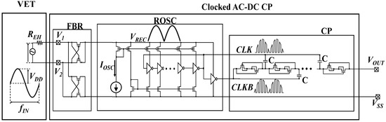
Figure 1.
Clocked AC-DC charge pump with vibration energy transducer (VET).
The effective threshold voltage is calculated by
where VT, S and IS are the thermal voltage, the silicon area given by CN, and the saturation current of each stage diode, respectively.
Equations (1)–(3) were presented in [14,15]. As the circuit parameters are included in such complicated equations, it is not easy to find an optimum design parameter set of C, N and diode size at the initial design phase when VDD and a target IOUT at VOUT are given. Therefore, estimation equations should be useful for designers who want to have an initial estimate for those design parameters. In other words, one can determine NOPT by running many SPICE simulations to find the peak point of IOUT. It must be beneficial for designers who want to identify the optimum number of stages, NOPT, to minimize the circuit area using a single calculation.
As Equations (1)–(3) are extracted based on the formula for DC-DC charge pumps, as shown in [24], we begin by determining the relationship between the minimum number of stages, NMIN, required to hold IOUT (N = NMIN) = 0, and the optimum number of stages, NOPT, required to minimize the circuit area, i.e., NOPT = 2 NMIN. Then, assuming that NOPT is proportional to NMIN for clocked AC-DC charge pumps as well as DC-DC charge pumps, NOPT = k NMIN, where k is a proportional coefficient determined empirically. As in [15], the following parameters were used to generate the curve in Figure 2a with Equations (1)–(3): f = 10 MHz, VDD = 0.5 V, VOUT = 2.5 V, VT = 34 mV, S = 10 pF, and IS = 10 nA. Under a given circuit area of S, IOUT was calculated with Equations (1)–(3). Figure 2a shows that the design with k~2.6 should provide high IOUT with a sufficient design margin when (4) is used for NMIN.
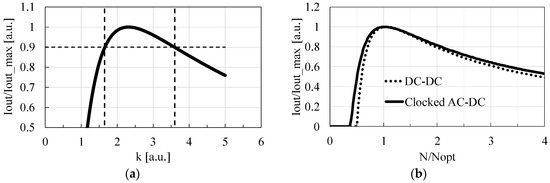
Figure 2.
k vs. IOUT for the clocked AC-DC charge pump (a) and N/NOPT vs. IOUT for the clocked AC-DC and DC-DC charge pumps with the same design parameters (b).
Even though k varies by 1 in a different parameter set, IOUT only decreases by 10%. Therefore, one can use the optimization Equation (5) together with Equation (4) to determine the number of stages of clocked AC-DC charge pumps, which is the most important product of this paper.
Figure 2b compares the sensitivity of IOUT on variation in N of the clocked AC-DC and DC-DC charge pumps whose design parameters are common. Note that the clocked AC-DC charge pump is less sensitive to variation in N than the DC-DC charge pump.
3. Validation of the Proposed Design
3.1. Validation of the Analytical IOUT-VOUT Equation
To validate the analytical IOUT-VOUT Equation (1) together with Equations (2)–(3), the measured data from the previously fabricated clocked AC-DC charge pump [15] were used. The design parameters were VDD = 0.5 V, N = 9, C = 10 pF, Is = 40 nA, VT = 34 mV and f = 4.8 MHz. Figure 3 compares the results from model 1 with the measured data. The discrepancy was within 10%, in the range of VDD = 0.4–0.8 V and VOUT = 1–3.5 V. Model 1 is therefore valid for design optimization based on Equation (1).
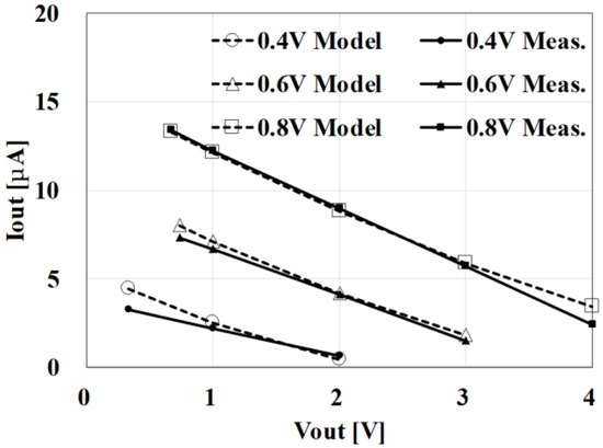
Figure 3.
Comparison of VOUT–IOUT between model Equations (1)–(3) and measured data for a previously fabricated clocked AC-DC charge pump [15].
To further validate the model Equations (1)–(3) at different numbers of stages, SPICE simulations were run under the conditions of f = 1 MHz, VDD = 0.5 V, VOUT = 2.0 V, VT = 34 mV, S = 1 nF, and IS = 10 nA. Figure 4 compares IOUT values when N is varied and S is constant. The model results are in good agreement with SPICE simulations. Figure 4 indicates that NOPT is 20, whereas (4) and (5) suggest NOPT is 25. Even though NOPT differed by 20%, the discrepancy in IOUT is as small as 2.5% thanks to the moderate curvature around the highest point in IOUT.
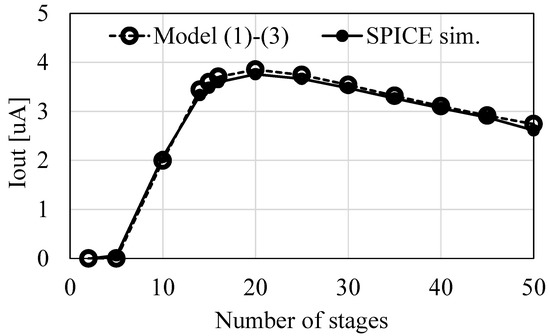
Figure 4.
Comparison of IOUT vs. N between the models and SPICE simulations.
3.2. Validation of the Optimization Equation
To validate whether the optimization equation (5) together with Equations (4) is effective for designing clocked AC-DC charge pumps, the parameters shown in Table 1 were investigated. C and N were calculated by a numerical simulation to have the highest IOUT under 1600 different combinations of design parameters based on Equations (1)–(3). C and N were also calculated based on Equations (4) and (5) and S = CN. Then, the values for IOUT calculated by those methods were compared. The results are shown in Figure 5a, which indicates that model Equations (4) and (5) for 800 of the combinations of parameters were in good agreement, to within 2% of numerical simulations using Equations (1)–(3), and that 98% of all the parameter combinations exhibited differences under 5%. When VT ln(fSVT/IS) becomes close to VDD, the error increases. As this situation occurs for NMIN > 100, such cases were omitted from the potential design conditions. Figure 5b shows that the discrepancy in values between models increases as the frequency increases to over 10 MHz. If a designer wishes to run clocked AC-DC charge pumps at high frequencies, Equations (4) and (5) may not be suitable.

Table 1.
Range of parameters used.
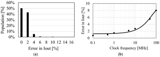
Figure 5.
Distribution of errors in IOUT between the two methods (a) and errors in IOUT vs. clock frequency (b).
4. Design Flow of Clocked AC-DC Charge Pumps
Figure 6 proposes a design flow for clocked AC-DC charge pumps. At step 1, the condition is defined where IOUTTarget is the target output current at VOUT. At step 2, NOPT is calculated by using Equations (4) and (5). At step 3, COPT value is calculated by S divided by NOPT. At step 4, IOUT0 is defined by IOUT with COPT and NOPT via Equations (1)–(3). At step 5, the scaling factor λ is identified. At step 6, the final values ISFIN, CFIN, and SFIN are scaled with λ. As a result, all the design parameters are determined. Those values are used for the initial SPICE simulation to verify whether the initial estimate is acceptable. Otherwise, the parameters may need to be updated.
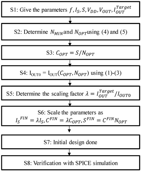
Figure 6.
Design flow for clocked AC-DC charge pumps.
To provide an example, we demonstrate the above design flow under the conditions of f = 1 MHz, VDD = 0.5 V, VOUT = 2.0 V, VT = 34 mV, S = 1 nF, and IS = 10 nA to obtain IOUT of 1 μA. NOPT was determined by Equations (4) and (5) to be 16. Then, COPT was calculated by S/NOPT to be 62.5 pF. IOUT0 was calculated by Equations (1)–(3) to be 7.0 μA, and therefore the scaling factor λ was 1/7 μA = 0.14 μA. As a result, ISFIN, CFIN, and SFIN were 1.4 nA, 8.8 pF and 140 pF, respectively. Figure 7 shows the waveform of the output current with SPICE. The IOUT was measured to be 0.97 μA, which is 3% smaller than the target IOUT. This result validates the proposed design method and flow.
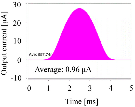
Figure 7.
Output current waveform simulated by SPICE and the average value IOUT.
5. Discussion
Electromagnetic VET has similar characteristics to magnetostrictive VET with respect to its relatively lower output open circuit voltage and low output impedance. Therefore, the design method proposed in this paper for clocked AC-DC charge pumps can also be applied to electromagnetic VET. The other types of VET—electrostatic, piezoelectric and triboelectric VET—require alternative types of power conversion than clocked AC-DC charge pump circuits.
SPICE simulation results showed that the clocked AC-DC charge pump circuit demonstrated in Section 4 has an input power, PINCP, of 8.8 μW, resulting in a charge pump power efficiency, ηCP ≡ POUTCP/PINCP of 23%. When a magnetostrictive VET with VDD = 0.5 V and an output resistance of 500 Ω is used, the maximum available power POUT_MAXET is calculated as 31 μW. Therefore, overall power efficiency ηSYS ≡ POUTCP/POUT_MAXET is estimated to be 8%.
In this paper, the impact of the parasitic capacitance of pumping capacitors (CP) on (1) was disregarded for simplicity. Design Equations (4) and (5) will need to be extended for cases where CP cannot be ignored. When clocked AC-DC charge pump circuits are designed considering the output impedance of VET, another design flow, such as that described in [25], will be required in addition to the design flow proposed in Figure 6. Further study is required to outline an optimum design to maximize power efficiency.
6. Conclusions
In this paper, we proposed Equations (4) and (5) to determine the number of stages which enables designers to obtain clocked AC-DC charge pumps with the minimum circuit area based on the previously formulated output voltage and current equation. In addition, a design procedure was also presented to determine the capacitance of each pump capacitor and the size of each rectifying device when the amplitude of the voltage generated by the vibration energy transducer, target output voltage, and target output current are given. The design method and flow are demonstrated and validated by SPICE simulation with 1600 different sets of design parameters. When a clocked AC-DC charge pump was designed based on the optimum equations to have an output current of 1 μA at 2.5 V from a vibration energy harvester with an AC voltage amplitude of 0.5 V, the discrepancy in the output current was just 3% from that based on a standard design method. Clocked AC-DC charge pump circuits with the minimum circuit area can be designed based on the equations and design flow proposed in this paper.
Author Contributions
Conceptualization, T.T.; methodology, J.Y. and T.T.; software, J.Y.; validation, J.Y. and T.T.; formal analysis, J.Y. and T.T.; investigation, J.Y. and T.T.; writing—original draft preparation, T.T.; writing—review and editing, J.Y. and T.T.; funding acquisition, T.T. All authors have read and agreed to the published version of the manuscript.
Funding
This research was partially funded by the Micron Foundation.
Acknowledgments
This work was supported by VDEC, Synopsys, Inc., Cadence Design Systems, Inc. Rohm Corp. and the Micron Foundation. The authors wish to thank M. Futagawa, H. Hirano and S. Ota for technical discussion.
Conflicts of Interest
The authors declare no conflict of interest.
References
- Mitcheson, P.D.; Yeatman, E.M.; Rao, G.K.; Holmes, A.S.; Green, T.C. Energy Harvesting From Human and Machine Motion for Wireless Electronic Devices. Proc. IEEE 2008, 96, 1457–1486. [Google Scholar] [CrossRef]
- Manoli, Y. Energy harvesting from devices to systems. In Proceedings of the 2010 Proceedings of ESSCIRC, Sevilla, Spain, 14–16 September 2010; pp. 27–36. [Google Scholar]
- Chao, L.; Tsui, C.-Y.; Ki, W.-H. A Batteryless Vibration-based Energy Harvesting System for Ultra Low Power Ubiquitous Applications. In Proceedings of the 2007 IEEE International Symposium on Circuits and Systems, New Orleans, LA, USA, 27–30 May 2007; pp. 1349–1352. [Google Scholar]
- Arakawa, Y.; Suzuki, Y.; Kasagi, N. Micro Seismic Power Generator Using Electret Polymer Film. Proc. PowerMEMS 2004, 187, 17. [Google Scholar]
- Ueno, T. Magnetostrictive vibrational power generator for battery-free IoT application. AIP Adv. 2019, 9, 035018. [Google Scholar] [CrossRef]
- Stanzione, S.; Van Liempd, C.; Van Schaijk, R.; Naito, Y.; Yazicioglu, R.F.; Van Hoof, C. A self-biased 5-to-60V input voltage and 25-to-1600µW integrated DC-DC buck converter with fully analog MPPT algorithm reaching up to 88% end-to-end efficiency. In Proceedings of the IEEE International Solid-State Circuits Conference, San Francisco, CA, USA, 17–21 February 2013; pp. 74–75. [Google Scholar] [CrossRef]
- Beeby, S.; Kazmierski, T.J. Energy Harvesting Systems: Principles, Modeling and Applications; Springer: Berlin/Heidelberg, Germany, 2010; Chapter 1. [Google Scholar]
- Rahimi, A.; Zorlu, O.; Külah, H.; Muhtaroglu, A. An interface circuit prototype for a vibration-based electromagnetic energy harvester. In Proceedings of the 2010 International Conference on Energy Aware Computing, Cairo, Egypt, 16–18 December 2010; pp. 1–4. [Google Scholar]
- Maurath, D.; Becker, P.F.; Spreemann, D.; Manoli, Y. Efficient Energy Harvesting With Electromagnetic Energy Transducers Using Active Low-Voltage Rectification and Maximum Power Point Tracking. IEEE J. Solid-State Circuits 2012, 47, 1369–1380. [Google Scholar] [CrossRef]
- Ulusan, H.; Gharehbaghi, K.; Zorlu, O.; Muhtaroglu, A.; Külah, H. A Fully Integrated and Battery-Free Interface for Low-Voltage Electromagnetic Energy Harvesters. IEEE Trans. Power Electron. 2014, 30, 3712–3719. [Google Scholar] [CrossRef]
- Wang, S.-W.; Ke, Y.-W.; Huang, P.-C.; Hsieh, P.-H. Electromagnetic Energy Harvester Interface Design for Wearable Applications. IEEE Trans. Circuits Syst. II Express Briefs 2018, 65, 667–671. [Google Scholar] [CrossRef]
- Karthaus, U.; Fischer, M. Fully integrated passive uhf rfid transponder ic with 16.7-μ minimum rf input power. IEEE J. Solid-State Circuits 2003, 38, 1602–1608. [Google Scholar] [CrossRef]
- Papotto, G.; Carrara, F.; Palmisano, G. A 90-nm CMOS Threshold-Compensated RF Energy Harvester. IEEE J. Solid-State Circuits 2011, 46, 1985–1997. [Google Scholar] [CrossRef]
- Kawauchi, H.; Tanzawa, T. A clocked AC-DC voltage multiplier for increasing the power conversion efficiency in vibration energy harvesting. In Proceedings of the IEICE General Conference, Tokyo, Japan, 20–23 March 2018; Available online: http://hdl.handle.net/10297/00025812 (accessed on 20 March 2018).
- Kawauchi, H.; Tanzawa, T. A 2V 3.8µW Fully-Integrated Clocked AC-DC Charge Pump with 0.5 V 500 Ω Vibration Energy Harvester. In Proceedings of the 2019 IEEE Asia Pacific Conference on Circuits and Systems (APCCAS), Bangkok, Thailand, 11–14 November 2019; pp. 329–332. [Google Scholar] [CrossRef]
- Shih, Y.; Otis, B.P. An Inductorless DC–DC Converter for Energy Harvesting With a 1.2-uW Bandgap-Referenced Output Controller. IEEE Trans. Circuits Syst. II Express Briefs 2011, 58, 832–836. [Google Scholar] [CrossRef]
- Kim, J.; Kim, J.; Kim, C. A Regulated Charge Pump With a Low-Power Integrated Optimum Power Point Tracking Algorithm for Indoor Solar Energy Harvesting. IEEE Trans. Circuits Syst. II Express Briefs 2011, 58, 802–806. [Google Scholar] [CrossRef]
- Peng, H.; Tang, N.; Yang, Y.; Heo, D. CMOS Startup Charge Pump with Body Bias and Backward Control for Energy Harvesting Step-Up Converters. IEEE Trans. Circuits Syst. I Regul. Pap. 2014, 61, 1618–1628. [Google Scholar] [CrossRef]
- Kim, J.; Mok, P.K.T.; Kim, C. A 0.15 V Input Energy Harvesting Charge Pump With Dynamic Body Biasing and Adaptive Dead-Time for Efficiency Improvement. IEEE J. Solid-State Circuits 2014, 50, 414–425. [Google Scholar] [CrossRef]
- Mondal, S.; Paily, R. An Efficient On-Chip Switched-Capacitor-Based Power Converter for a Microscale Energy Transducer. IEEE Trans. Circuits Syst. II Express Briefs 2015, 63, 254–258. [Google Scholar] [CrossRef]
- Liu, X.; Huang, L.; Ravichandran, K.; Sanchez-Sinencio, E. A Highly Efficient Reconfigurable Charge Pump Energy Harvester with Wide Harvesting Range and Two-Dimensional MPPT for Internet of Things. IEEE J. Solid-State Circuits 2016, 51, 1302–1312. [Google Scholar] [CrossRef]
- Goeppert, J.; Manoli, Y. Fully Integrated Startup at 70 mV of Boost Converters for Thermoelectric Energy Harvesting. IEEE J. Solid-State Circuits 2016, 51, 1716–1726. [Google Scholar] [CrossRef]
- Fuketa, H.; O’Uchi, S.-I.; Matsukawa, T. Fully Integrated, 100-mV Minimum Input Voltage Converter with Gate-Boosted Charge Pump Kick-Started by LC Oscillator for Energy Harvesting. IEEE Trans. Circuits Syst. II Express Briefs 2017, 64, 392–396. [Google Scholar] [CrossRef]
- Tanzawa, T. An Analytical Model of Charge Pump DC-DC Voltage Multiplier Using Diodes. IEICE Trans. Fundam. Electron. Commun. Comput. Sci. 2017, 1137–1144. [Google Scholar] [CrossRef]
- Tanzawa, T. Design of DC-DC switched-capacitor voltage multiplier driven by DC energy transducer. In Proceedings of the 2014 21st IEEE International Conference on Electronics, Circuits and Systems (ICECS), Marseille, France, 7–10 December 2014; pp. 327–330. [Google Scholar]
- Tanzawa, T. An Optimum Design for Integrated Switched-Capacitor Dickson Charge Pump Multipliers with Area Power Balance. IEEE Trans. Power Electron. 2014, 29, 534–538. [Google Scholar] [CrossRef]
- Peters, C.; Kessling, O.; Henrici, F.; Ortmanns, M.; Manoli, Y. CMOS Integrated Highly Efficient Full Wave Rectifier. In Proceedings of the IEEE International Symposium on Circuits and System, New Orleans, LA, USA, 27–30 May 2007; pp. 2415–2418. [Google Scholar] [CrossRef]
- Haddad, P.-A.; Gosset, G.; Raskin, J.-P.; Flandre, D. Automated Design of a 13.56 MHz 19 µW Passive Rectifier With 72% Efficiency Under 10 µA load. IEEE J. Solid-state Circuits 2016, 51, 1290–1301. [Google Scholar] [CrossRef]
- Tokuda, S.; Tanzawa, T. Toward a Minimum-Operating-Voltage Design of DC-DC Charge Pump Circuits for Energy Harvesting. In Proceedings of the 2019 IEEE International Symposium on Circuits and Systems (ISCAS), Sapporo, Japan, 26–29 May 2019; pp. 1–4. [Google Scholar] [CrossRef]
- Tanzawa, T. A Behavior Model of an On-Chip High Voltage Generator for Fast, System-Level Simulation. IEEE Trans. Very Large Scale Integr. (VLSI) Syst. 2011, 20, 2351–2355. [Google Scholar] [CrossRef]
- Ye, J.; Tanzawa, T. An Optimum Circuit Design of clocked AC-DC charge pumps. In Proceedings of the IEICE General Conference, Higashihiroshima, Japan, 17–20 March 2020; Available online: http://hdl.handle.net/10297/00027066 (accessed on 17 March 2020).
- Levacq, D.; Liber, C.; Dessard, V.; Flandre, D. Composite ULP diode fabrication, modelling and applications in multi-Vth FD SOI CMOS technology. Solid-State Electron. 2004, 48, 1017–1025. [Google Scholar] [CrossRef]


Publisher’s Note: MDPI stays neutral with regard to jurisdictional claims in published maps and institutional affiliations. |
© 2020 by the authors. Licensee MDPI, Basel, Switzerland. This article is an open access article distributed under the terms and conditions of the Creative Commons Attribution (CC BY) license (http://creativecommons.org/licenses/by/4.0/).