Article

Design and Development of BTI Model and 3D InGaAs HEMT-Based SRAM for Reliable and Secure Internet of Things Application

Department of Electrical and Computer Engineering, 3301 South Dearborn Street, Siegel Hall, Illinois Institute of Technology, Chicago, IL 60616, USA
*
Author to whom correspondence should be addressed.
These authors contributed equally to this work.
Electronics 2020, 9(3), 469; https://doi.org/10.3390/electronics9030469
Submission received: 25 January 2020 / Revised: 22 February 2020 / Accepted: 6 March 2020 / Published: 11 March 2020

Abstract

:
It is broadly accepted that the silicon-based CMOS has touched its scaling limits and alternative substrate materials are needed for future technology nodes. An Indium-Gallium-Arsenide ( I n G a A s )-based device is well situated for further technology nodes. This material also has better mobility of the electrons and holes for the high performance and real-time system design. The improved mobility helps to increase the operating frequency of the device which is useful for Internet of Things (IoT) applications. However, I n G a A s -based High Electron Mobility Transistors (HEMT) limits the reliability of the device due to the presence of dangling bonds at the channel–gate insulator interfaces. Weak dangling-bonds get broken under electric stress, and positive hydrogen atoms are trapped into the oxide. This charge trapping depends on the material parameters and device geometry. In this paper, the existing Bias-Temperature-Instability (BTI) model is modified based on the material parameters and device geometry. Charge trapping and annealing constants are the most critical BTI model parameters that are modeled and evaluated based on different HEMT material parameters. The proposed model was compared to experimental and TCAD simulation results. The proposed model has been used for lifetime prediction of the InGaAs HEMT-based Static Random-Access Memory (SRAM) cell because it is used to store and process the information in the IoT applications.

1. Introduction

Wireless sensor networks (WSNs) have been extensively used as devices for information collection and decision making. These capabilities have expanded the scope of applications of WSNs in many fields including Internet of Things (IoT), healthcare, search and rescue where sensor nodes are deployed at remote locations and under extreme conditions [1]. Power-consumption is one of the important challenges that restrict the efficiency of WSN since sensor nodes are battery operated. Hence, life time prediction of the VLSI chips used for WSN circuits has become a necessity. Speed is another design requirement for WSN circuits which are required to operate at high frequencies. Since MOSFET no longer supports high-frequency operation, High Electron Mobility Transistors (HEMT) provide an alternative solution to achieve high-performance circuit design for WSNs [2]. HEMT has been used to design satellite receivers and sensor nodes [3,4]. Some compound semiconductor materials are used to increase the operating frequency of HEMT such as Gallium-Nitride ( G a N ) and Indium-Gallium-Arsenide ( I n G a A s ). In I n G a A s -based HEMT, the indium material provides extra strain to increase the mobility of electrons and holes. These semiconductor devices use high-k dielectric materials in order to establish strong insulation of the gate terminal. This helps to reduce the gate leakage current for the low power circuit design. Unlike the conventional bulk-based MOSFET, the high-k dielectric materials in HEMT establish a weak interafce with the bulk material. Therefore, more dangling bonds are generated in HEMT than MOSFET in order to strengthen the contact at the bulk dielectric interface. ( S i O 2 / S i ) [5].
When HEMT devices are operated under electrical stress, the dangling-bonds get broken, and positive hydrogen atoms get trapped inside the gate-insulator, which increases the threshold voltage of the HEMT. Consequently, the HEMT threshold voltage increases which causes a decrease in the operating frequency. Such effects are further escalated at higher temperatures due to the Bias-Temperature-Instability (BTI) which is one of the main reliability degradation sources in HEMT. Other reliability degradation sources include Time-Dependent Dielectric Breakdown (TDDB) and Hot Carrier Injection (HCI) [6]. Therefore, an efficient HEMT-based circuit design should carefully consider the effects of those sources. Due to the complexity of developing a physical VLSI chip, CAD tools are used to model and simulate the behavior of VLSI circuits. Models should incorporate all the reliability degradation sources in order to obtain an accurate simulation of the VLSI circuit under their effects. The Reaction–Diffusion (RD) model [7] can be used to model the increase in the threshold voltage of the HEMT. The RD model is based on using electrochemical reactions and activation energies to represent the interface state [7]. Reliability models should also account for the various device parameters and geometrical properties and therefore they should be modified accordingly based on the device under test.
The primary components of an IoT system are a data converter, a transmitter, and a receiver [1]. These components can be designed using logic circuits and storing elements such as Static Random-Access Memory (SRAM) [8]. Hence, the proposed reliability model for HEMT can be tested on SRAM. SRAM is considered to be the fundamental storing element occupying more than 80% of the on-chip area of the processor. Since HEMT is used for high-frequency SRAM design, the prediction of its lifetime becomes necessary [9]. In this paper, an I n G a A s -based SRAM is designed and analyzed to evaluate its stability under BTI stress. Based on this analysis, a BTI model for SRAM lifetime prediction has been proposed, and further, it is used for an SRAM circuit simulation using SystemVerilog-based modeling and the HSPICE EDA tool. The highlights of the proposed works are as follows:
  • Design and simulation of the I n G a A s -based HEMT;
  • Calibration of simulation models and HEMT with experimental data;
  • Proposed a PBTI/NBTI model for HEMT;
  • Proposed model is modified according to the material parameters;
  • Use of proposed model for 6T SRAM cell design.
The rest of the paper is organized as follows: In Section 2, the state-of-the-art BTI models are discussed. In Section 3, the proposed I n G a A s -based HEMT design is discussed. In Section 4, simulation setup, model calibration with experimental results, and design are proposed. In Section 5, the 6T SRAM cell is briefly described and simulation results are discussed. In Section 6, a spice equivalent BTI model for the I n G a A s -based HEMT is discussed. In Section 7, the simulation results of the proposed model are discussed. Section 8 concludes the work.

2. State-Of-The-Art BTI Models

It was already mentioned in a previous study, that the trapping of the charge carrier in the gate insulator due to the NBTI/PBTI can be defined by the RD-model [7]. Due to the unclear nature of NBTI/PBTI, more realistic RD-models that better incorporate the effects of those sources have been proposed. Kufluoglu et al. [10] has proposed a model where the transistor structure and scaling-based compact NBTI model were included. It shows similar characteristics with the numerical simulation results despite the superiority of this model to all other kinds of transistor structures, the model parameters were not experimentally determined. Furthermore, the electron/hole generation and annealing parameters were used but the model did not include the device structure and experimental data. Another RD-based model has been proposed by Islam et al. [11,12], which showed the passivation/depassivation effects of the Si-H bond by using the initial charge density, electron/hole generation constant, and annealing constant. This model, however, did not show the geometrical effect on NBTI/PBTI. For circuit simulation purposes, this model was modified and applied for 65 nm CMOS technology [13]. When BTI is induced, the trap charge density was found to be dependent on the diffusion constant. Therefore, the RD model is further modified to include the diffusion length. This model used the default values for the hole/electron generation and annealing constant [14]. The same model was further modified for silicon body tied FinFET [15].
Some statistical reliability models were proposed for FinFET and SRAM cells and used to investigate the NBTI effects [16]. An NBTI framework for 20 nm node devices was presented by Mishra et al. [17]. The stress generated by BTI is found to be more significant than PBTI stress. NBTI reduces the inversion charges and degrades the electron and hole mobility. It is due to the Coulomb scattering and depends on the applied gate voltage, temperature, and stress time [16,17]. In these works, they also assumed that the generated interface state is designing a substrate gate interface bond with their energy distribution.
In this work, we have modified the existing model given by Kufluoglu et al. [10] and proposed a new geometry-based BTI model device for N-type I n G a A s HEMT (FinFET). The electron–hole generation constant and different parameter values are calculated for the I n G a A s - A l 2 O 3 interface. Due to the model dependency on the hydrogen diffusion consistent, this constant has been calculated for the I n G a A s - A l 2 O 3 interface. Further, the effectiveness of the proposed model has been tested with the TCAD simulator, and results are verified with state-of-the-art experimental results.

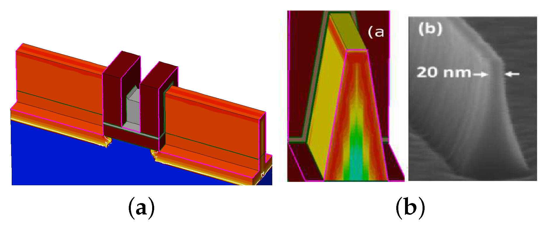
3. Proposed InGaAs HEMT

Figure 1 shows the architecture of the I n G a A s -based HEMT [18]. The real physical device operation was simulated using a process equivalent TCAD simulation [19]. To design I n 0.53 G a 0.47 A s A l 2 O 3 interface, I n P was deposited over the insulator, and over it, an I n G a A s layer was deposited for device formation. Then, a A l 2 O 3 gate insulator layer was deposited at the top. Tin material was deposited over the I n G a A s layer which formed the gate layer. After the device design, a simulation-based device characterization was done using the S d e v i c e TCAD simulator [19]. The values used for R O N and I O F F are 180 Ω/μm and 100 nA/μm, respectively, are obtained at V D S = 0.5 V and calibrated as per the experimental data [20]. Other important parameters are shown in Table 1. Figure 2 shows the current–voltage characteristics of a device with W f i n = 22 nm, and L g = 30 nm. Figure 2 and Table 1 both show the calibration results with experimental data [20].
To understand the BTI effect in the proposed device, we need to understand the bulk–oxide and oxide–metal interface properties. The properties of this interface depend on the gate oxide materials such as S i O 2 , H f O 2 , L a 2 O 3 , A l 2 O 3 , and T a S i O x . The unbounded states, the band-decomposed charge density corresponding to the bandgap pinning energy interval are shown in a 3D plot by Kim et al. [21]. This 3D plot can be used to determine the exact location and the number of dangling bonds at the I n G a A s and A l 2 O 3 insulator interface. The unbounded states are localized at the existing coordinated Aluminum ( A l ) atoms which have bonded with two Oxygen ( O s ) atoms and one Hydrogen (H) atom. In amorphous bulk, A l 2 O 3 and A l primarily have four bonds with O, as shown in Figure 3. These dangling bonds change the electrical properties of a device and increase the density of the existing interface trapped charges ( N i t ).
Active depletion charge density is used to understand the interface properties which gives the device reliability information. The active interface charge in the depletion region can be measured using a quasi-static and high-frequency capacitance–voltage model. Figure 4 shows bi-directional capacitance–voltage (CV) curves for different gate insulator interfaces for I n G a A s -based HEMT [22]. These data are taken from published experimental work [22]. Figure 4 shows the initial charge density for L a 2 O 3 -based gate insulator is lower because the trivalent oxides A l 2 O 3 and L a 2 O 3 have fewer dangling bonds. Having fewer dangling bonds reduces the interracial state. However, L a 2 O 3 is very unstable material [22], hence we are using A l 2 O 3 as a gate insulator material in the proposed I n G a A s -based HEMT. The next element of the proposed work is an SRAM cell for the IoT applications, which is explained in the next section.

4. BTI Effects on 6T SRAM Cell

Figure 5 shows a 6T SRAM cell, which is designed by the I n G a A s -based HEMT. It can also be called FinFET for circuit applications. The design parameters (Fin Number (NF)) of the proposed SRAM transistors are as follows; driver(PD) NF = 4, Access(A) NF = 2, and Pull-Up (PU) NF = 4. Data retention stability under standby condition is analyzed by Static Noise Margin (SNM), and read stability is analyzed by Read Noise Margin (RNM). Synopsys TCAD-mixed-mode simulator has been used for the I n G a A S device-based circuit simulation. The 6T SRAM cell was analyzed in both standby and read mode operations using the two-stage NBTI and degradation models in [19]. The trap charge density under three-year stress in standby mode operation is shown in Figure 6. The figure shows a single driver transistor for the two-stage NBTI model because symmetric inverters design the 6T SRAM cell and NBTI affects the PMOS transistors only. In the degradation model, the effect of BTI is plotted for both NMOS and PMOS [19,23]. TCAD simulation results show a significant change in the trap charge density.
The SNM butterfly curves of the proposed SRAM cell is shown in Figure 7a. We take a standard Gaussian doping and initial N I T = c o n = 4 × 10 12 . The N I T increases with three-year stress. A similar result is also shown for the RNM (as shown in Figure 7b). These variations can not be considered under the most of the available spice–circuit simulators. Hence, most of the circuit simulators can not predict the reliability of the chip (in terms of the lifetime). The MOSERA model bases reliability simulation can be performed in the H-SPICE simulator, but it uses a fundamental power–law model. Hence, the proposed BTI model, which is developed especially for I n G a A s -based FinFET, can be used in circuit simulation.

5. Proposed BTI Model for HEMT

HEMT is a three-dimensional (3D) device with three trapping regions; two of them are from side walls and one from the top. Top and side walls show one-dimensional (1D) trap-induced BTI, whereas the corners show two-dimensional (2D) trap-induced BTI, as shown in Figure 8.
We have already discussed that the RD model is used for the electric’s stress-induced trapping. The RD model follows the time-dependent power–law model [10]. In the RD model, the shift in NMOS parameters induced by PBTI is represented by the breaking of the hydrogen passivated substrate material bonds in the I n G a A s - - A l 2 O 3 interface. The total charge trap density at I n G a A s - - A l 2 O 3 interface due to BTI (PBTI and NBTI) is given by [10]:
d N I T d t = k f N 0 N I T k r N I T N H ( x = 0 , t )
d N I T d t = D d N H ( x , t ) d x | x = 0 + δ 2 N H ( x , t ) d t
where N 0 is the initial trap charge density and N I T shows the total interface charge due to the BTI in the I n G a A s - - A l 2 O 3 interface. N I T depends on the rate at which H atoms are generated. Therefore, k f is the H generation rate and k r is the annealing rate. This parameter is used in the recovery phase. Some time N I T may approach N 0 because the diffusion process is slower than ionization and annealing [13]. Annealing is responsible for the removal of hydrogen from the I n G a A s - A l 2 O 3 interface. The diffusion process can also be considered to be taking place in the quasi-steady-state condition of this reaction. Therefore, d N I T / d t 0 Equation (1) may be simplified as:
k f ( N 0 N I T ) k r = N H 0 N I T
Using this relation in Equation (2), the total trap charge density can be modeled by:
d N I T d t = D H N H 0 D H t = D H t k f k r ( N 0 N H N I T )
Equation (1) shows that the trap charge density increases with the net reaction. Diffusion in FinFET is a process that happens in 2D at the corners and in 1D at the top and sidewalls. Hence, Equation (1) cannot be used to describe this process. For a more realistic representation, diffusion in the 1D and 2D are explained first. Assuming that H is one interface yields to the equation N I T ( t ) = N H ( r , t ) d 3 r . It is previously mentioned that the rate at which H atoms are released is much greater than the diffusion rate. The hydrogen profile represented by ( D H t ) 0.5 is shown on the left side of Figure 8b. Therefore, the 1D diffusion of hydrogen on a plane surface in the x direction is derived as:
N I T 1 D ( t ) = 0 D H t N H 0 1 x D H t d x
by putting values from Equation (3) into Equation (5), we obtain the solution:
N I T 1 D ( t ) = k f N 0 2 k r ( D H t ) 0.25
Further, The hydrogen diffusion at the corners is a 2D process, as shown in Figure 8. There, the corresponding hydrogen diffusion profile is shown on the right in Figure 8b, which is circular and makes only a 1/4 circles at each corner, which is obtained by the circumference of the circle [10].
N I T 2 D ( t ) = 1 4 0 D H t N H 0 1 r D H t 2 π r d r
where r is the radius of the circle which is equivalent to the thickness of the oxide. Now putting the values from Equation (3) into Equation (7)
N I T 2 D ( t ) = π k f N 0 12 r k r ( D H t ) 0.5
Similarly, the above explanation can be used to estimate the diffusion of hydrogen on a 2D surface. In the prescribed structure, the side and top walls show 1D diffusion, whereas the two corners show the 2D diffusion interface, as shown in Figure 8a,b. Hence, the interface state density generated by BTI is given by:
N I T s t r e s s = 2 0 D H t N H 0 ( 1 x D H t ) d x + 0 D H t N H 0 ( 1 y D H t ) d y + 2 4 0 D H t N H 0 ( 1 r D H t ) 2 π r d r
By substituting r = t o x E O T and W into Equation (1), we can write:
N I T s t r e s s ( t ) = k f N 0 2 k r ( D H t ) 1 2 + π ( D H t ) 9 W t o x 1 6
where, k f and k r are the rates of generation of H 2 i.e., electron/hole and k r is the annealing rate. The shift of the trap threshold is described by:
V t h = α q C o x N I T s t r e s s
where α is a multiplication factor that depends on the type of device structure, temporal parameter degradation caused by BTI depends on the physical properties of the channel and type of gate oxide.
We did not work on the recovery model and we have used the recovery model as given by Reis et al. [24]. The recovery process happens in two stages: The first stage involves a fast recovery caused by H 2 atoms inside the gate oxide. The second stage involves a slow recovery caused by H 2 due to the back diffusion from gate oxide to I n G a A s (bulk or channel). The number of annealed traps consists of two parts represented by the recombination of H 2 in A l 2 O 3 and the back diffusion of H 2 in the gate. At the end of the stress (time t 0 ), the number of generated trap charges is given by the following equation and it becomes zero if k f = 0 :
N I T r e c d t = k r ( N H 0 N H ) ( N I T 0 N I T )
where, N H 0 is the hydrogen concentration generated after stress at time t 0 and C is a constant [7]. Therefore, the change in threshold voltage after recovery is given by:
V t h = α q C o x N I T r e c
where α is a multiplication factor that depends on the type of device structure, Equations (11) and (13) describe the stress and recovery process of the trap charges caused by NBTI/PBTI for I n G a A s -based HEMT, respectively.

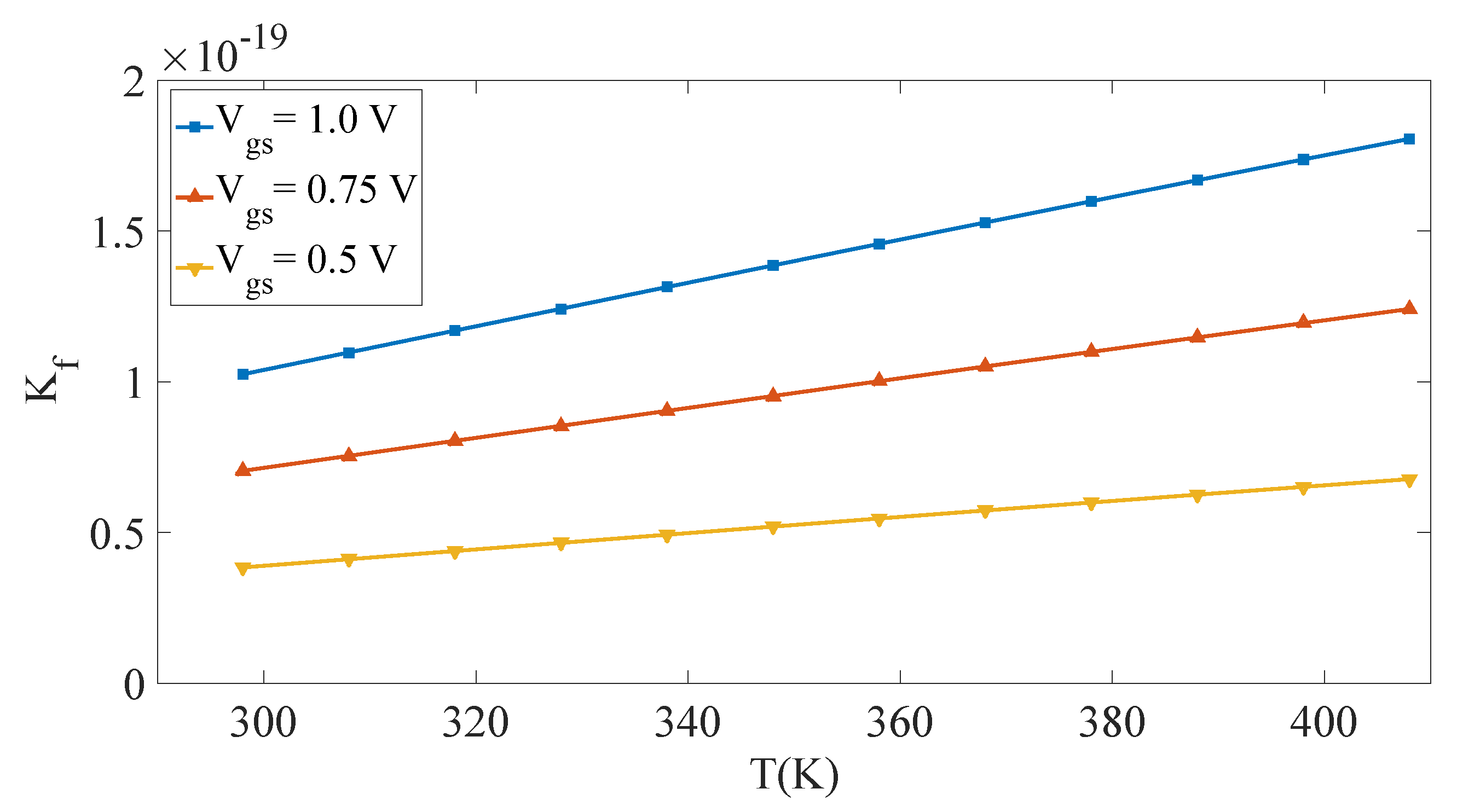
6. Modeling of Charge Generation Constant

In this section, a mathematical model of the electron/hole generation constant ( K f ) for I n G a A s –FinFET (HEMT) is derived. The following expression conventionally gives the K f constant:
K f = σ E e f f P e f f
where σ is the electron/hole capture cross-section, E e f f is the effective oxide field across the gate oxide, and P e f f is the effective potential. Such factors were all investigated in previous material level studies [25,26]. σ depends on the activation energy, temperature, doping concentration, and the layer thickness [25]. The electron capture cross-section area is an important parameter for K f . If the capture cross-section is more than K f , is also more. The electron capture cross-section areas are greater, by 3× of magnitude, than the hole capture cross-section. The electron capture cross-sectional area is very large and has a value that ranges from 10 15 to 10 14 . It depends on the recombination center [25,26]. The value of σ for I n G a A s -based HEMT can be given by:
σ = σ e x p ( E B K T )
where E B is the activation energy, σ is the pre-exponential factor, K is the Boltzmann constant, and T is the temperature in Kelvins. The values of the pre-exponential factor σ and the activation energy E B for an I n G a A s substrate and insulator A l 2 O 3 -based HEMT are derived in this work. The default value of σ used in the literature is in the range of 6 × 10 15 to 1 × 10 17 [25], and the values of σ for G a A s and I n G a A s are 6 × 10 15 and 1 × 10 20 , respectively [25]. Hence, these values have been employed in different simulation experiments to find the optimal value for the I n G a A s - - A l 2 O 3 interface. The change of the electron capture cross-section with respect to temperature variation is depicted in Figure 9 which shows that K f is directly proportional to the temperature and that K f increases as V g s increases. The effective oxide field ( E e f f ) and the effective potential P e f f depends on the gate voltage ( V g s ), the threshold voltage ( V t h ), and the oxide capacitance ( C o x ). Hence, k f can be modeled as:
k f = σ e x p ( E B K T ) e x p ( E o x E 0 ) C o x ( V g s V t h )
k r = σ e x p ( E B K T ) C o x ( V g s V t h )
The annealing constant K r also depends on the oxide electric field, the gate voltage, and the threshold voltage of the device. For K r , V g s is either zero or has a positive value for apposite stress. The values of E o x and E 0 are always zero. The parameter values extracted from the simulation results and are listed in Table 2.

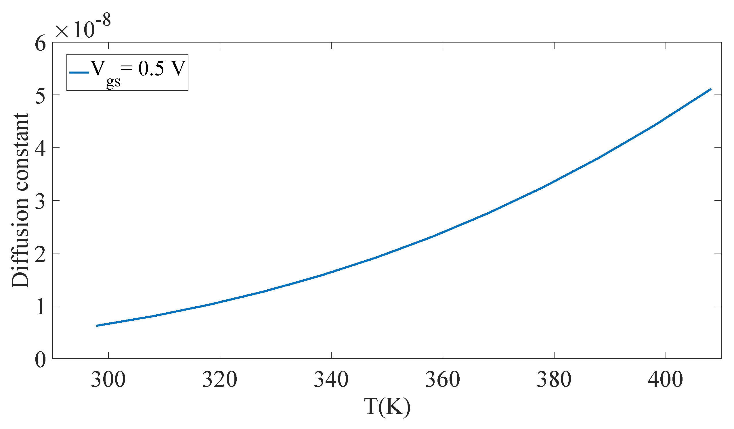
Modeling of Hydrogen Diffusion Constant

Another important factor for BTI-induced trapping is Hydrogen diffusion constant ( D H ). As per experimental data, the value of E B for the I n G a A s A l 2 O 3 interface is in the range of 0.05 to 0.066 eV [5,25]. Temperature is important parameter for the diffusion constant. These parameters were extracted for the BTI model using different experimental data in these papers [5,25]. The Hydrogen diffusion constant D 0 is given by:
D H = D 0 e x p ( E a K T )
where E a is the activation energy, K is the Boltzmann constant, and T is the temperature. The value of D 0 for H 2 diffusion in A l 2 O 3 ranges from 1.5 × 10 5 to 1 × 10 6 as per the state-of-the-art experimental results [5,25]. The diffusion constant values for varying temperatures are shown in Figure 10 which shows that the diffusion constant is highly dependent on the temperature. Therefore, the temperature is an important parameter required to estimate K f , K r , and D H . All the related parameters for the I n G a A s -based HEMT are shown in Table 2.

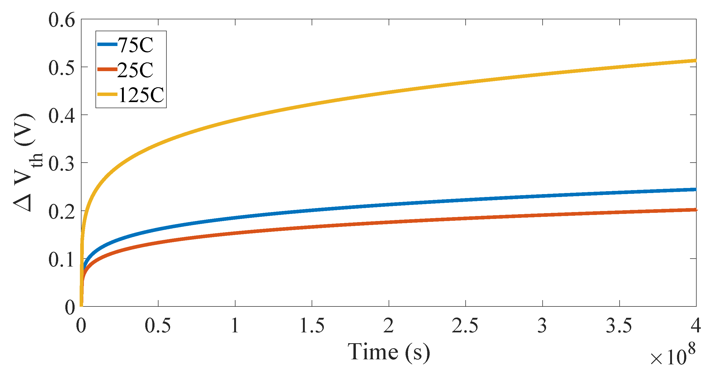
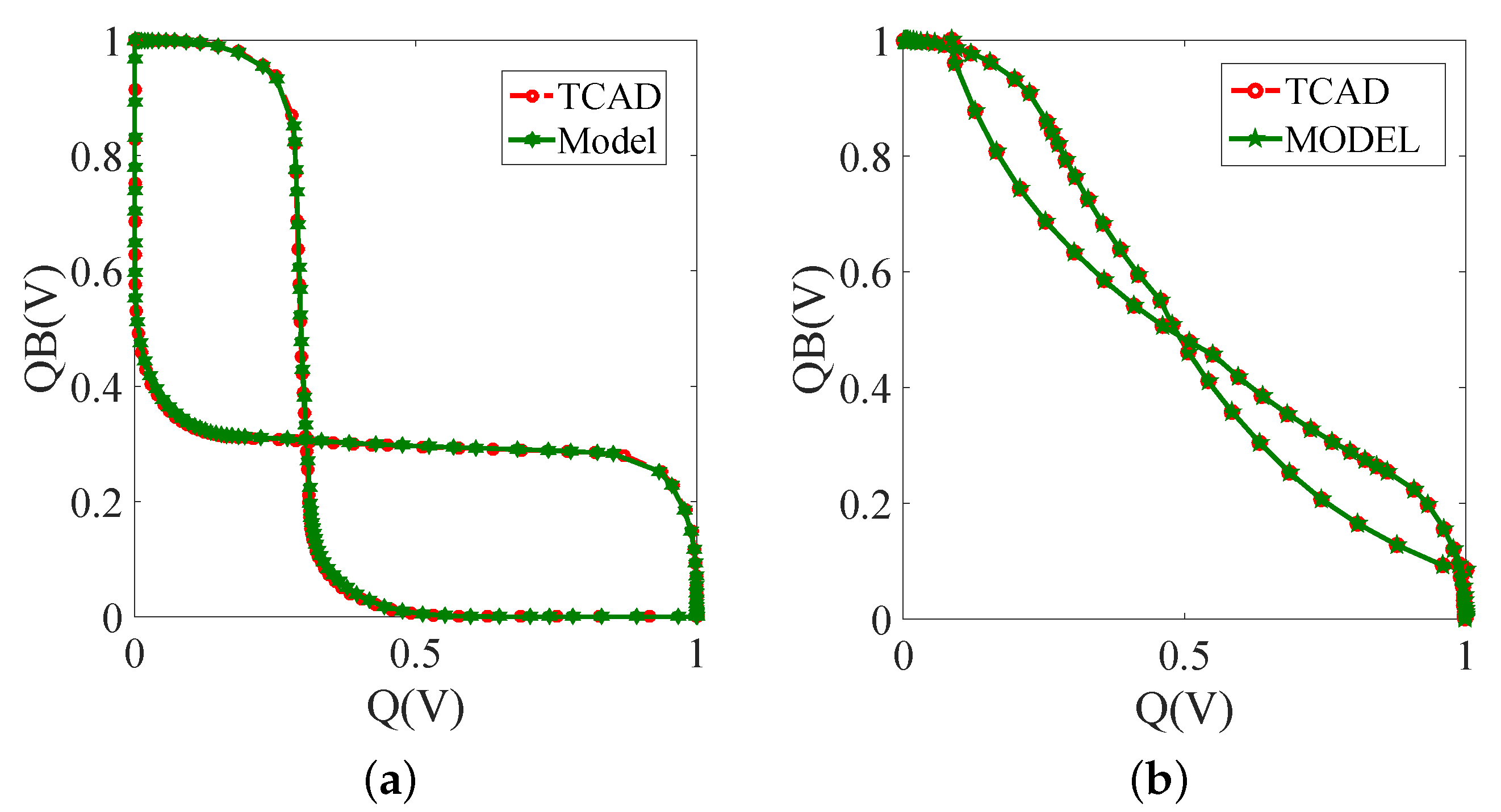
7. Model Verification and Circuit Simulation

To verify the proposed model, modeling results are compared with the experimental result. The first model is verified for silicon-based MOSFET (Figure 11) and further, it is verified for 3D InGaAs HEMT. It is also used to predict the lifetime prediction of the SRAM. The required parameters are calculated from the model file for the model. The flat band voltage and the vertical gate oxide ( E o x ) are calculated from the BSIM model then the change in the threshold voltage ( V t h ) due to PBTI is calculated. All calculated and optimized parameters are shown in Table 2. The comparative results for the model with the experimental results for the change in the threshold voltage are shown in Table 3 [27,28,29,30]. All results are calculated for different device dimensions, but one of the available studies is very similar to the proposed work, hence, we made a detailed comparison with the similar study. Hence, the proposed model has been further verified using the experimental results for 10-year stress and different temperatures values obtained from data given by Franco et al. [30]. The stress voltage from −1 V to maximum V g s has been applied for the P-FinFET. The initial trap density ( N 0 ) from −1 V to maximum V g s was extracted from [30]. The hole capture constant ( K f ) is calculated using the proposed model and calibrated as per the literature. The simulation results for 10-year stress are shown in Figure 12 [30] which clearly shows that PBTI is strongly affected by the vertical electric field has a linear relationship with V g s . A similar plot at a l o g scale is shown in Figure 13 [30].
Circuit simulation was conducted using the 6T SRAM cell for testing purposes. The total change in the trap charge density for three-year stress and the corresponding shift in the threshold voltage was calculated. The simulation flow and strategy are shown in Figure 14. The initial charge density and the other parameters are calculated from the device model file. In HSPICE, the parameters given by the . p a r a m command in the spice net-list are used to calculate the change in the threshold voltage due to BTI i.e., v t h = v t h 0 + Δ V t h . The . a l t e r command used to simulate the second stage gives the final simulation output. Figure 15 shows the comparative results of the proposed model and TCAD simulation for a 6T SRAM cell. The SNM and RNM results of the 6T SRAM cell are calibrated according to the TCAD simulation results.

8. Conclusions

Static Random-Access Memory (SRAM) is used as a data storing and processing element in Wireless Sensor Networks and the Internet of Things (IoT) applications. Hence, SRAM should be a high-performance, reliable element. In this work, We have analyzed the stability of the 6T using the two-stage NBTI and degradation models under the deference electric stress. It is revealed from the results that NBTI affects almost 20% of the stability compared to the conventional target design only in the three-year stress. Also, the RD-based BTI model was modified for the 3D I n G a A s -based HEMT and presented as a proposed BTI model for circuit simulation. This model has been used for lifetime prediction of the 6T SRAM cell. The BTI model parameters have been calculated, extracted, and optimized using material parameters and device geometrical dimensions. The modified model contains all the main characteristics of the reaction–diffusion model. The proposed model can be used to predict DC stress for electrical stresses. Consequently, this model can be utilized to predict BTI under real device and circuit working conditions.

Author Contributions

Conceptualization, N.Y.; Investigation, Writing-original draft, Writing-review and editing, M.A.; Editing, K.K.C.; Funding acquisition and supervisor. All authors have read and agreed to the published version of the manuscript.

Funding

This research was funded by the Industrial Core Technology Development Program of MOTIE/KEIT, KOREA grant number 10083639.

Acknowledgments

We thank our colleagues from KETI and KEIT who provided insight and expertise that greatly assisted the research and greatly improved the manuscript. This work is also supported by the Industrial Core Technology Development Program of MOTIE/KEIT, KOREA [# 10083639].

Conflicts of Interest

No conflict of interest.

References

  1. Kabashkin, I.; Kundler, J. Reliability of sensor nodes in wireless sensor networks of cyber physical systems. Procedia Comput. Sci. 2017, 104, 380–384. [Google Scholar] [CrossRef]
  2. Qian, Q.; Lei, J.; Wei, J.; Zhang, Z.; Tang, G.; Zhong, K.; Zheng, Z.; Chen, K.J. 2D materials as semiconducting gate for field-effect transistors with inherent over-voltage protection and boosted ON-current. NPJ 2D Mater. Appl. 2019, 3, 1–9. [Google Scholar] [CrossRef]
  3. Halfaya, Y.; Bishop, C.; Soltani, A.; Sundaram, S.; Aubry, V.; Voss, P.L.; Salvestrini, J.P.; Ougazzaden, A. Investigation of the performance of HEMT-based NO, NO2 and NH3 exhaust gas sensors for automotive antipollution systems. Sensors 2016, 16, 273. [Google Scholar] [CrossRef] [PubMed]
  4. Sharma, P.; Sharma, N.; Gupta, R.; Jogi, J. Simulating Optical Behavior of Nano Dimensional InAlAs/InGaAs HEMT for IoT Applications. In Proceedings of the 2018 UKSim-AMSS 20th International Conference on Computer Modelling and Simulation, Cambridge, UK, 27–29 March 2018; pp. 181–185. [Google Scholar]
  5. Joshi, K.; Mukhopadhyay, S.; Goel, N.; Mahapatra, S. A consistent physical framework for N and P BTI in HKMG MOSFETs. In Proceedings of the 2012 IEEE International Reliability Physics Symposium, Anaheim, CA, USA, 15–19 April 2012; p. 5A-3. [Google Scholar]
  6. Oktyabrsky, S.; Peide, D.Y. Fundamentals of III-V Semiconductor MOSFETs; Springer: New York, NY, USA, 2010. [Google Scholar]
  7. Alam, M.A. A critical examination of the mechanics of dynamic NBTI for PMOSFETs. In Proceedings of the IEDM’03 International Technical Digest Electron Devices Meeting, Washington, DC, USA, 8–10 December 2003; pp. 4–14. [Google Scholar]
  8. Abbasizadeh, H.; Kim, S.Y.; Samadpoor Rikan, B.; Hejazi, A.; Khan, D.; Pu, Y.G.; Hwang, K.C.; Yang, Y.; Kim, D.I.; Lee, K.Y. Design of a 900 MHz Dual-Mode SWIPT for Low-Power IoT Devices. Sensors 2019, 19, 4676. [Google Scholar] [CrossRef] [PubMed] [Green Version]
  9. Puttaswamy, K.; Loh, G.H. 3D-integrated SRAM components for high-performance microprocessors. IEEE Trans. Comput. 2009, 58, 1369–1381. [Google Scholar] [CrossRef]
  10. Kufluoglu, H.; Alam, M.A. Theory of interface-trap-induced NBTI degradation for reduced cross section MOSFETs. IEEE Trans. Electron Devices 2006, 53, 1120–1130. [Google Scholar] [CrossRef]
  11. Lee, H.; Lee, C.H.; Park, D.; Choi, Y.K. A comprehensive modeling of dynamic negative-bias temperature instability in PMOS body-tied FinFETs. IEEE Electron Device Lett. 2006, 27, 281–283. [Google Scholar]
  12. Islam, A.E.; Kufluoglu, H.; Varghese, D.; Mahapatra, S.; Alam, M.A. Recent issues in negative-bias temperature instability: Initial degradation, field dependence of interface trap generation, hole trapping effects, and relaxation. IEEE Trans. Electron Devices 2007, 54, 2143–2154. [Google Scholar] [CrossRef] [Green Version]
  13. Wang, W.; Reddy, V.; Krishnan, A.T.; Vattikonda, R.; Krishnan, S.; Cao, Y. Compact modeling and simulation of circuit reliability for 65-nm CMOS technology. IEEE Trans. Device Mater. Reliab. 2007, 7, 509–517. [Google Scholar] [CrossRef]
  14. Alam, M.A.; Kufluoglu, H.; Varghese, D.; Mahapatra, S. A comprehensive model for PMOS NBTI degradation: Recent progress. Microelectron. Reliab. 2007, 47, 853–862. [Google Scholar] [CrossRef]
  15. Ma, C.; Li, B.; He, F.; Zhang, X.; Lin, X. A novel Negative Bias Temperature Instability model for nanoscale Finfet. In Proceedings of the 16th IEEE International Symposium on the Physical and Failure Analysis of Integrated Circuits, Suzhou, China, 6–10 July 2009; pp. 117–121. [Google Scholar]
  16. Wang, Y.; Cotofana, S.D.; Fang, L. Statistical reliability analysis of NBTI impact on FinFET SRAMs and mitigation technique using independent-gate devices. In Proceedings of the 2012 IEEE/ACM International Symposium on Nanoscale Architectures, Amsterdam, The Netherlands, 4–6 July 2012; pp. 109–115. [Google Scholar]
  17. Mishra, S.; Wong, H.Y.; Tiwari, R.; Chaudhary, A.; Rao, R.; Moroz, V.; Mahapatra, S. TCAD-Based Predictive NBTI Framework for Sub-20-nm Node Device Design Considerations. IEEE Trans. Electron Devices 2016, 63, 4624–4631. [Google Scholar] [CrossRef]
  18. Yadav, N.; Shah, A.P.; Beohar, A.; Vishvakarma, S.K. Source drain Gaussian doping profile analysis for high ON current of InGaAs based HEMT. In Proceedings of the 2017 International Conference on Electron Devices and Solid-State Circuits, Hsinchu, Taiwan, 18–20 October 2017; pp. 1–2. [Google Scholar]
  19. Synopsys, T. SDEVICE Manual, Release H-2013.03; Synopsys: Zurich, Switzerland, 2013. [Google Scholar]
  20. Vardi, A.; del Alamo, J.A. Sub-10-nm Fin-Width Self-Aligned InGaAs FinFETs. IEEE Electron Device Lett. 2016, 37, 1104–1107. [Google Scholar] [CrossRef]
  21. Kim, E.J.; Chagarov, E.; Cagnon, J.; Yuan, Y.; Kummel, A.C.; Asbeck, P.M.; Stemmer, S.; Saraswat, K.C.; McIntyre, P.C. Atomically abrupt and unpinned Al2O3/In0.53Ga0.47As interfaces: Experiment and simulation. J. Appl. Phys. 2009, 106, 124508. [Google Scholar] [CrossRef]
  22. Weijtens, C. Reduction of oxide charge and interface-trap density in MOS capacitors with ITO gates. IEEE Trans. Electron Devices 1992, 39, 1889–1894. [Google Scholar] [CrossRef]
  23. Parihar, N.; Goel, N.; Mukhopadhyay, S.; Mahapatra, S. BTI analysis tool Modeling of NBTI DC, AC stress and recovery time kinetics, nitrogen impact, and EOL estimation. IEEE Trans. Electron Devices 2017, 65, 392–403. [Google Scholar] [CrossRef]
  24. Reis, R.; Cao, Y.; Wirth, G. Circuit Design for Reliability; Springer: New York, NY, USA, 2015. [Google Scholar]
  25. Mitonneau, A.; Mircea, A.; Martin, G.; Pons, D. Electron and hole capture cross-sections at deep centers in gallium arsenide. Rev. Phys. Appl. 1979, 14, 853–861. [Google Scholar] [CrossRef]
  26. Saks, N.S.; Ancona, M.G. Determination of interface trap capture cross sections using three-level charge pumping. IEEE Electron Device Lett. 1990, 11, 339–341. [Google Scholar] [CrossRef] [Green Version]
  27. Deora, S.; Bersuker, G.; Kim, T.; Kim, D.; Hobbs, C.; Kirsch, P.; Sahoo, K.; Oates, A. Positive bias instability in gate-first and gate-last InGaAs channel n-MOSFETs. In Proceedings of the 2014 IEEE International Reliability Physics Symposium, Waikoloa, HI, USA, 1–5 June 2014; p. 3C-5. [Google Scholar]
  28. Cartier, E.; Frank, M.M.; Ando, T.; Rozen, J.; Narayanan, V. PBTI in InGaAs MOS capacitors with Al2O3/HfO2/TiN gate stacks: Interface-state generation. In Proceedings of the 2018 IEEE International Reliability Physics Symposium, Burlingame, CA, USA, 11–15 March 2018; p. 5A-4. [Google Scholar]
  29. Li, Y.; Di, S.; Jiang, H.; Huang, P.; Wang, Y.; Lun, Z.; Shen, L.; Yin, L.; Zhang, X.; Du, G.; et al. Insight into PBTI in InGaAs nanowire FETs with Al2O3 and LaAlO3 gate dielectrics. In Proceedings of the 2016 IEEE International Electron Devices Meeting, San Francisco, CA, USA, 3–7 December 2016; p. 36-5. [Google Scholar]
  30. Franco, J.; Kaczer, B.; Waldron, N.; Roussel, P.J.; Alian, A.; Pourghaderi, M.A.; Ji, Z.; Grasser, T.; Kauerauf, T.; Sioncke, S.; et al. RTN and PBTI-induced time-dependent variability of replacement metal-gate high-k InGaAs FinFETs. In Proceedings of the 2014 IEEE International Electron Devices Meeting, San Francisco, CA, USA, 15–17 December 2014; pp. 20–22. [Google Scholar]
Figure 1. Proposed device (a) architecture and (b) aliment of the fin as per the experimental data [20].
Electronics 09 00469 g001
Figure 2. Calibration of the transfer characteristics of device with W f = 22 nm and L g = 30 nm with the experimental data (blue symbol graph) [20].
Electronics 09 00469 g002
Figure 3. The amorphous oxide interface ( I n G a A s - A l 2 O 3 ) shows the initial structure of oxide bulk placed on the clean semiconductor–oxide interface.
Electronics 09 00469 g003
Figure 4. Capacitance voltage (CV) curves of different materials at 1 KHz and 1 MHz frequencies (AC analysis).
Electronics 09 00469 g004
Figure 5. 6T SRAM cell design using proposed I n G a A s -based HEMT (FinFET).
Electronics 09 00469 g005
Figure 6. Change in trap charge carrier concentration due to NBTI and PBTI in 6T Static Random-Access Memory (SRAM) cell transistor in standby mode of operation: (a) using two stage NBTI model and (b) using degradation model (NBTI and PBTI).
Electronics 09 00469 g006
Figure 7. Change in 6T SRAM cell stability due to NBTI and PBTI: (a) Static Noise Margin (SNM) and (b) Read Noise Margin (RNM).
Electronics 09 00469 g007
Figure 8. Cross section of the interface at the fin, 1D from the side walls and corners contributes the 2D trap-induced Bias-Temperature-Instability (BTI) effect.
Electronics 09 00469 g008
Figure 9. Hold generation constant for the I n G a A s - - A l 2 O 3 interface for varying temperatures (T).
Electronics 09 00469 g009
Figure 10. Diffusion constant for I n G a A s - - A l 2 O 3 interface with varying temperatures.
Electronics 09 00469 g010
Figure 11. NBTI model results compared with measured data for S i O 2 and S i interface of a MOSFET.
Electronics 09 00469 g011
Figure 12. PBTI model results compared to the measured data for the I n G a A s to A l 2 O 3 interface.
Electronics 09 00469 g012
Figure 13. PBTI model results compared to the measured data for the I n G a A s to A l 2 O 3 interface in log scale.
Electronics 09 00469 g013
Figure 14. Proposed flow chart for the SRAM circuit simulation in a spice-based circuit simulation environment using the proposed model.
Electronics 09 00469 g014
Figure 15. Model calibration results for the 6T SRAM cell stability: (a) SNM; (b) RNM.
Electronics 09 00469 g015
Table 1. Device parameters for Indium-Gallium-Arsenide ( I n G a A s )-based High Electron Mobility Transistors (HEMT) as per the experimental results [20].
Operating voltage V D D [V]0.5
Operating overdrive =2/3 * V D D [V]0.33
EOT [nm]1.8
Operating E o x [mV/cm]2
H f i n [nm]35
W f i n [nm]10
L G a t e [nm]30
PBTI time exponent (n)0.1
Δ V t h ( t = 10 Y ) @ O p . E o x [mV]118
Δ N e f f ( t = 1 s ) @ O p . E o x [cm−2]2 × 10¹¹
Table 2. Extracted BTI model parameters for I n G a A s - - A l 2 O 3 interface.
σ 1 × 10 16
K 1.38 × 10 23
E O T 1.8 nm
K A l 2 O 3 9
ϵ 0 8.85 × 10 14
K r = K r 0 e E A K r k T K r 0 = 9.9 × 10 7
D H 0 9.56 × 10⁻¹¹ cm2/s
E a 0.2 eV
E o x 2 eV
E 0 0.5 eV
N 0 2 × 10 11
ξ 0.58
E B 0.054 eV
Table 3. Comparison of the modeling results with the experiment results.
S.No. Δ V th Stress Time(s) t ox Ref.
10.1510002.0[27]
20.12510004.2[28]
30.1510003.5[29]
40.1510001.8 nm[30]
40.1510001.8 nmCalculated in this work

