Abstract
Epitaxial in situ doped Si0.73Ge0.27 alloys were grown selectively on patterned bulk Ge and bulk Si wafers. Si0.73Ge0.27 layers with a surface roughness of less than 3 nm were demonstrated. Selectively grown p+Si0.73Ge0.27 layers exhibited a resistivity of 3.5 mΩcm at a dopant concentration of 2.5 × 10¹⁹ boron atoms/cm3. P+/n diodes were fabricated by selectively growing p+- Si0.73Ge0.27 on n-doped bulk Ge and n-doped Si wafers, respectively. The geometrical leakage current contribution shifts from the perimeter to the bulk as the diode sizes increase. Extracted near midgap activation energies are similar to p+/n Ge junctions formed by ion implantation. This indicates that the reverse leakage current in p+/n Ge diodes fabricated with various doping methods, could originate from the same trap-assisted mechanism. Working p+/n diodes on Ge bulk substrates displayed a reverse current density as low as 2.2·10−2 A/cm2 which was found to be comparable to other literature data. The layers developed in this work can be used as an alternative method to form p+/n junctions on Ge substrates, showing comparable junction leakage results to ion implantation approaches.
1. Introduction
Currently Ge based field effect transistor (FET) devices are researched due to their potential for low voltage operation stemming from the superior hole and electron mobility in Ge as compared to Si. A critical aspect in fabricating such devices is junction formation and control of junction leakage current. Junctions on bulk Ge have been traditionally formed with ion implantation and a subsequent anneal. The need for highly doped, shallow and abrupt junctions on Si has been met with the introduction of selective epitaxially grown in situ doped SiGe layers [1,2,3,4,5,6,7,8]. Junctions on bulk Ge have been traditionally formed with ion implantation and a subsequent anneal to activate the implanted dopants [9,10]. However, ion implantation damages the Ge crystal [11,12]. This creates the need for a high temperature treatment to anneal out the defects and recrystallize Ge [13,14,15,16]. A high heating rate can induce structural damage while a low annealing time might not fully crystallize the implanted region, resulting in defect formation that will affect the junction leakage current [17]. Reaching high doping concentrations (>1020 cm−3) can give rise to defect formations that affect dopant diffusion [18]. Recently a report has shown the potential of sequential 3D integration with Ge devices [19]. Such fabrication methods require a reduced thermal budget, usually determined by an upper limit in the area of 600 °C [20,21]. Selective epitaxy of in situ doped SiGe is an implantation-free and temperature-flexible process. It has therefore, the potential to address the challenges outlined above. In [22] epitaxial in situ n+ doped SiGe with concentrations from 20% to 100% Ge are grown on virtual Ge substrates to achieve low source/drain contact resistance (ρc). It is shown that 20% Ge content in the in situ doped SiGe alloy exhibits approximately two orders of magnitude lower ρc than the ion implanted SiGe with the same Ge content. In [23] a simulation study of As doped Si0.75Ge0.25 embedded stressors in a Ge FinFET fabricated on germanium-on-insulator (GOI) substrates is presented. The authors show a three-fold improvement in the device current at the ON state (ION), achieved with 25% Ge in the SiGe stressor.
This work investigates the feasibility of selectively grown, in situ doped p+-Si0.73Ge0.27 layers as a source/drain junction material. Planar p+/n diodes were fabricated on SiO2 patterned, bulk n-Ge substrates using selective epitaxy of p+- Si0.73Ge0.27. A benchmark towards other junctions on Ge bulk is performed. Insights on junction leakage that can be helpful for further device integration are provided by the electrical characterization of the p+/n diodes. The thermal budget for the process presented here was set by the epitaxial growth temperature of 650 °C. The layers can potentially be integrated in germanium-on-insulator (GOI) substrates and in sequential 3D integration where the process budget for dopant activation is limited.
2. Materials and Methods
Selective epitaxial growth of in situ doped Si0.73Ge0.27 was performed on n-Si wafers (525 μm, As doped, resistivity = 20–40 Ohm·cm, supplied by Westec) and on n-Ge wafers (460 μm, Sb doped, resistivity = 0.05–0.25 Ohm·cm, supplied by Umicore). A description of the process flow and the resulting diode structures on Si and Ge substrates is shown in Figure 1. The openings towards Ge or Si were patterned on a 200 nm SiO2 with i-line optical lithography. Dry etch was used to remove all but ~20 nm SiO2 layer on top of the surface openings. The remaining SiO2 layer was removed during pre-epitaxy surface cleaning. For Si surfaces, ex situ surface treatment was performed in a 3:1 mixture of H2SO4 (CAS 7664-93-9, 95–97%, BASF/Merck) / H2O2 (CAS 7722-84-1, >=35–<50%, Sigma-Aldrich Sweden AB) followed by 1% HF (CAS 7664-39-3, 5% wt, BASF/Sigma-Aldrich Sweden AB) diluted in H2O. Ge surfaces require a different ex situ cleaning approach that does not involve H2O2 which is a Ge etchant. In this work a 1% HF surface clean in an automated wet etch spray tool followed by a rinse and dry step was conducted prior to loading in the epitaxial reactor. All epitaxial growth was performed in an ASM Epsilon 2000 reduced pressure chemical vapor deposition (RPCVD) reactor at a constant pressure of 20 Torr in H2 ambient. In situ surface preparation was common for both Si and Ge substrates and was conducted at 800 ºC in H2 for 10 min inside the RPCVD chamber. This temperature was well below the melting point of Ge and potential Ge surface reflow issues were thus avoided. The selective epitaxial growth of SiGe was performed at 650 °C under 20 Torr with H2 (20 slm, 10% in N2, CAS 1333-74-0, <=100%, AGA Gas AB/Air Liquide) as the carrier gas. The gas precursors for Si and Ge species are H2SiCl2 (60 sccm, CAS 4109-96-0, <=100%, AGA Gas AB/Air Liquide) and GeH4 (10 sccm, CAS 7782-65-2, 10% in H2, AGA Gas AB), respectively. The in situ doping was achieved B2H6 (80 sccm, CAS 019287-45-7, 1% in H2, AGA Gas AB) for p+SiGe. A 10 s 1% HF dip was employed prior to the metal contact definition. A 100 nm TiW and 500 nm Al metal stack was deposited by physical vapor deposition (PVD) for contacting the fabricated diodes.
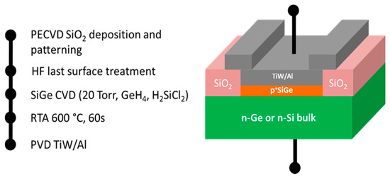
Figure 1.
The p+/n diode fabrication flow is shown in the left. The resulting device is depicted on the right. Each device is accessed from the top via a TiW/Al metal stack and the bottom of the bulk substrate via the measurement unit’s chuck.
3. Results and Discussion
3.1. Layer Characterization
Atomic force microscopy (AFM) was used for surface roughness and step height profile measurements. The AFM image is shown in Figure 2. The p+- Si0.73Ge0.27 layers show a root mean square (RMS) surface roughness of < 3 nm. Spectroscopic ellipsometry (SE) was used for layer thickness and Ge content measurements. The growth rate of the p+- Si0.73Ge0.27 on Ge was 45 nm/min. Secondary ion mass spectroscopy (SIMS) was performed to determine the dopant concentration and the Ge content in the Si0.73Ge0.27 alloy. The SIMS profiles are shown in Figure 3. Dopant concentration is 2.5 × 10¹⁹ B atoms per cm3. Ge content is 27% in agreement with the result from SE. A summary of the layer characterization results is presented in Table 1. X-ray diffraction (XRD) measurements were performed on SiGe layers grown on 1.7 μm of Ge strain relaxed buffer substrates (SRB). The Ge SRB substrates were grown in house as reported in [24].
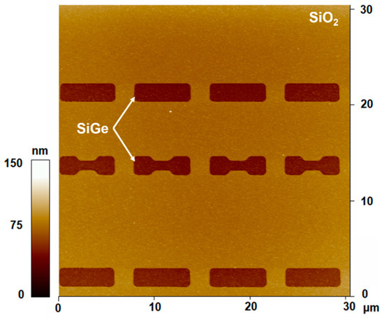
Figure 2.
Atomic force microscopy (AFM) image (35 μm × 35 μm) of the p+-Si0.73Ge0.27 film grown on the substrate openings of an SiO2 masked Ge strain relaxed buffer (SRB) wafer. The root mean square (RMS) surface roughness is 2.4 nm. The growth is selective to SiO2.
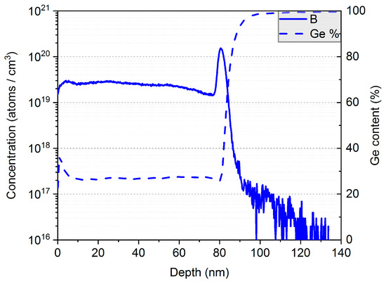
Figure 3.
Secondary ion mass spectroscopy (SIMS) analysis on 80 nm thick p+-Si0.73Ge0.27 layer grown on Ge SRB. Boron dopant concentration is 2.5 × 10¹⁹ atoms/cm3. The peak for the B concentration around 80 nm layer depth is due to dopant segregation at the SiGe/Ge interface. The Ge content of the SiGe layer is 27%.

Table 1.
p+-Si~0.7Ge~0.3 layer properties. For the growth rate, all three methods are in agreement at ~45 nm/min. Similarly, Ge content as deducted from the three methods is ~30%.
In Figure 4 the ω-2θ XRD profile of 120 nm thick p+-Si0.73Ge0.27 grown on Ge SRB is shown. The Si peak corresponds to the Si bulk on which the Ge SRB was grown. The XRD peak suggests Ge content of 27%.
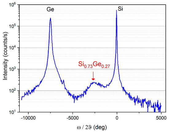
Figure 4.
X-ray diffraction results of the 120 nm thick p+-Si0.73Ge0.27 layer grown on Ge. The peak corresponding to Si0.73Ge0.27 does not show well defined fringes due to layer relaxation.
3.2. Electrical Characterization and Analysis
Square shaped diodes with varying sizes were measured. The junction quality between the epitaxially grown p+-Si0.73Ge0.27 layer and the substrate was evaluated by examining the reverse leakage current (IR). The thickness of the p+-Si0.73Ge0.27 films was 40 nm for both Ge and Si substrates. IR values were extracted at a reverse voltage of 1 V for all diode sizes. In Figure 5 the current (I) –voltage (V) characteristics of diodes on Ge bulk with areas from 4 μm2 to 104 μm2 are shown.
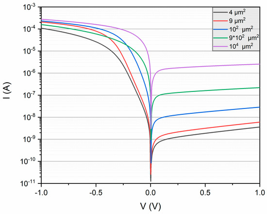
Figure 5.
Current (I) versus applied voltage (V), for p+-Si0.7Ge0.3 on n-type Ge diodes with area from 4 μm2 to 104 μm2.
The forward current is in the same order of magnitude for all the diodes and is limited by the series resistance of the back contact to the wafer as well as the bulk resistance of the wafer itself (Figure 1). The ideality factor is ~1.3 as extracted from the 4 μm2 and 9 μm2 diodes. Leakage current density of 2.2·10−2 A/cm2 is achieved for the 104 μm2 diode. Figure 6 shows IR as a function of the perimeter (P) length for Ge and Si diodes. The reverse leakage current is about two decades higher for Ge devices due to the higher intrinsic carrier concentration in Ge compared to Si. For squared shaped diodes IR can be expressed as the sum of the leakage current per unit area (IA) and the leakage current per unit perimeter (IP) as follows [25,26,27,28]:
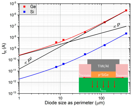
Figure 6.
Area and perimeter dependent diode leakage current for Ge and Si substrates. In the insert the two main leakage mechanisms are graphically depicted. The black lines show the reverse current as a function of only area (P2) or perimeter (P). Red and blue lines depict IR for Ge and Si using Equation (1) and fitting parameters IA and IP.
The solid black lines show the reverse current behavior as a function of only area (P2) or perimeter (P). The solid red and blue lines in Figure 6 display IR using Equation (1) with IA and IP as fitting parameters. Area and perimeter components of IR for Ge and Si substrates are found to be:
For small area diodes, with a perimeter of 8 µm or 12 µm, the perimeter component of the leakage current dominates IR. This occurs both on Si and Ge substrates although the effect is slightly more pronounced on Ge, possibly due to higher surface state density for SiO2/Ge interfaces compared to the SiO2/Si interfaces. The higher perimeter leakage on Ge substrates has been reported on p+/n-diode fabricated by ion implantation [29].
For diodes with a perimeter length of 40 µm and above, the area component dominates IR and for the largest diodes (104 µm2), the area component is >20x the perimeter component. Therefore, the largest diodes were further characterized by evaluating the temperature dependence of IR. Figure 7 shows an Arrhenius plot of IR for Ge and Si diodes in the temperature range of −50 °C to 100 °C. The extracted activation energy was 0.42 eV for Ge and 0.48 eV for Si, respectively.
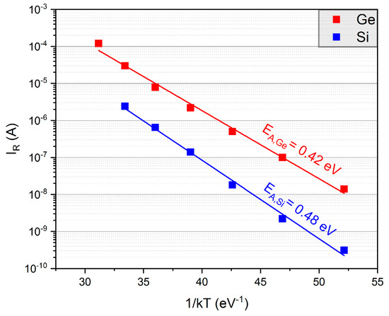
Figure 7.
Arrhenius plot of the leakage current ΙR versus 1/kT for 104 μm2 diodes where the bulk leakage dominates.
The activation energies are consistent with area dependent leakage currents caused by trap assisted generation/recombination mechanisms for both Ge and Si diodes [30,31]. For these activation energies, the trap centers can potentially originate at the interface between the p+-Si0.73Ge0.23 layer and the substrates without eliminating the possibility for defects in the bulk wafers.
Reverse current density values extracted at 1 V from similarly sized p+/n diodes (~104 μm2) on Ge reported in the literature are shown in Table 2 for comparison [32,33,34,35,36,37]. The literature data were chosen in order to cover as broad an area as possible in terms of doping techniques, annealing approaches and substrates. Diodes fabricated with ion implantation (I/I), spin-on-dopant (SOD) techniques as well as various anneals (laser annealing—LA, ELA and rapid thermal annealing—RTA) are included. The sole experimental data reported so far with a non-ion implantation approach can be found in [33] where a spin-on-dopant (SOD) technique is used. The leakage current of the Ge diodes in this work is on a par with p+/n SOD junctions reported in [33] that have also been laser annealed. In addition, leakage current densities reported here are within the range of ion implanted p+/n diodes reported in [32,33,34,35]. Our work shows similar levels of leakage current density as in the ion implantation junction studies. The near midgap activation energies for p+/n diodes (with B ion implantation for the p+ region) reported by Duffy et al. in [30], are close to the activation energies in this work. This indicates that the reverse leakage current in p+/n germanium diodes has the same origin for the various doping methods in Table 2.
Table 2.
Leakage current density comparison between a 104 μm2 diode fabricated with selective epitaxy (this work) and other published data of similarly sized diodes (where that information was available). The reverse current values were graphically extracted at 1V.
4. Conclusions
In situ doped Si0.73Ge0.27 layers have been successfully grown on n-Ge bulk wafers at 650 ºC. In-situ boron doped p+- Si0.73Ge0.27 layers exhibit a resistivity of 3.5 mΩcm and a dopant concentration of 2.5·1019 cm−3. For both Ge and Si diodes the dominant leakage current component shifts from perimeter to area as the diode sizes increase. The extracted near midgap activation energy is similar to p+/n Ge junctions formed by ion implantation methods. This indicates that the reverse leakage current in p+/n Ge diodes could originate from the same trap-assisted mechanism for various doping methods. A leakage current density of 2.2·10−2 A/cm2 for 104 μm2 diode area is achieved on Ge wafers with an RTA anneal of 600 ºC. This result is on a par with the literature data from ion implantation and spin-on-dopant approaches, showing that selective epitaxy of in situ doped SiGe layers is a promising candidate for low temperature junction formation on Ge substrates.
Author Contributions
Conceptualization, K.G., A.A. (Ahmad Abedin) and A.A. (Ali Asadollahi); methodology, K.G., A.A. (Ahmad Abedin), A.A. (Ali Asadollahi) and P.-E.H.; investigation, K.G.; data curation, K.G. and P.-E.H.; writing—original draft preparation, K.G.; writing—review and editing, K.G., Ahmad Abedin and P.-E.H.; visualization, K.G.; supervision, P.E.H. and M.Ö.; All authors have read and agreed to the published version of the manuscript.
Funding
This work was supported by the Swedish Foundation for Strategic Research (SSF).
Acknowledgments
EAG Laboratories are acknowledged for the PCOR-SIMSSM analysis.
Conflicts of Interest
The authors declare no conflicts of interest.
References
- Hartmann, J.M.; Benevent, V.; Barnes, J.P.; Veillerot, M.; Lafond, D.; Damlencourt, J.F.; Morvan, S.; Prévitali, B.; Andrieu, F.; Loubet, N.; et al. Mushroom-free selective epitaxial growth of Si, SiGe and SiGe: B raised sources and drains. Solid State Electron. 2013, 83, 10–17. [Google Scholar] [CrossRef]
- Hartmann, J.M.; Py, M.; Barnes, J.P.; Prévitali, B.; Batude, P.; Billon, T. Low temperature boron and phosphorous doped SiGe for recessed and raised sources and drains. J. Cryst. Growth 2011, 327, 68–77. [Google Scholar] [CrossRef]
- Wang, G.; Abedin, A.; Moeen, M.; Kolahdouz, M.; Luo, J.; Guo, Y.; Chen, T.; Yin, H.; Zhu, H.; Li, J.; et al. Integration of highly-strained SiGe materials in 14nm and beyond nodes FinFET technology. Solid-State Electron. 2015, 103, 222–228. [Google Scholar] [CrossRef]
- Wang, G.L.; Moeen, M.; Abedin, A.; Kolahdouz, M.; Luo, J.; Qin, C.L.; Zhu, H.L.; Yan, J.; Yin, H.Z.; Li, J.F.; et al. Optimization of SiGe selective epitaxy for source/drain engineering in 22 nm node complementary metal-oxide semiconductor (CMOS). J. Appl. Phys. 2013, 114, 123511. [Google Scholar] [CrossRef]
- Hartmann, J.M.; Benevent, V.; Damlencourt, J.F.; Billon, T. A benchmarking of silane, disilane and dichlorosilane for the low temperature growth of group IV layers. Thin Solid Films 2012, 520, 3185–3189. [Google Scholar] [CrossRef]
- Radamson, H.H.; Kolahdouz, M.; Ghandi, R.; Hållstedt, J. Selective epitaxial growth of B-doped SiGe and HCl etch of Si for the formation of SiGe: B recessed source and drain (pMOS transistors). Thin Solid Films 2008, 517, 84–86. [Google Scholar] [CrossRef]
- Qi, Y.; Peng, J.; Lo, H.-C.; Holt, J.R.; Willemann, M.; Gaire, C.; Evans, S.; Flanagan, P.; Yu, H.; Hu, O.; et al. In-Situ Boron Doped SiGe Epitaxy Optimization for FinFET Source/Drain. ECS Trans. 2016, 75, 265–272. [Google Scholar] [CrossRef]
- Chang, W.H.; Ota, H.; Maeda, T. Achieving low parasitic resistance in Ge p-channel metal–oxide–semiconductor field-effect transistors by ion implantation after germanidation. Appl. Phys. Express 2015, 8, 054201. [Google Scholar] [CrossRef]
- Hubbard, G.S.; Haller, E.E.; Hansen, W.L. Ion implanted n-type contact for high-purity germanium radiation detectors. IEEE Trans. Nucl. Sci. 1977, 24, 161–164. [Google Scholar] [CrossRef]
- Riepe, G.; Protić, D. High-purity germanium detectors with both contacts made by ion-implantation. Nucl. Instrum. Methods 1979, 165, 31–34. [Google Scholar] [CrossRef]
- Decoster, S.; Vantomme, A. Implantation-induced damage in Ge: Strain and disorder profiles during defect accumulation and recovery. J. Phys. Appl. Phys. 2009, 42, 165404. [Google Scholar] [CrossRef]
- Impellizzeri, G.; Mirabella, S.; Grimaldi, M.G. Ion implantation damage and crystalline-amorphous transition in Ge. Appl. Phys. A 2011, 103, 323–328. [Google Scholar] [CrossRef]
- Luo, X.; Wang, G.; Xu, J.; Duan, N.; Mao, S.; Liu, S.; Li, J.; Wang, W.; Chen, D.; Zhao, C.; et al. Impact of Ge pre-amorphization implantation on forming ultrathin TiGe x on both n- and p-Ge substrate. Jpn. J. Appl. Phys. 2018, 57, 07MA02. [Google Scholar] [CrossRef]
- Liu, J.; Mehta, S. Effect of Ge Pre-amorphization on Junction Characteristics for Low Energy B Implants. MRS Online Proc. Libr. Arch. 2000, 610, B4.6.1–B4.6.6. [Google Scholar] [CrossRef]
- Kelly, R.A.; Liedke, B.; Baldauf, S.; Gangnaik, A.; Biswas, S.; Georgiev, Y.; Holmes, J.D.; Posselt, M.; Petkov, N. Epitaxial Post-Implant Recrystallization in Germanium Nanowires. Cryst. Growth Des. 2015, 15, 4581–4590. [Google Scholar] [CrossRef]
- Tsai, M.H.; Wu, C.-T.; Lee, W.-H. Activation of boron and recrystallization in Ge preamorphization implant structure of ultra shallow junctions by microwave annealing. Jpn. J. Appl. Phys. 2014, 53, 041302. [Google Scholar] [CrossRef]
- Hsueh, F.-K.; Lee, Y.-J.; Lin, K.-L.; Current, M.I.; Wu, C.-Y.; Chao, T.-S. Amorphous-Layer Regrowth and Activation of P and As Implanted Si by Low-Temperature Microwave Annealing. IEEE Trans. Electron Devices 2011, 58, 2088–2093. [Google Scholar] [CrossRef]
- Sgourou, E.N.; Panayiotatos, Y.; Vovk, R.V.; Kuganathan, N.; Chroneos, A. Diffusion and Dopant Activation in Germanium: Insights from Recent Experimental and Theoretical Results. Appl. Sci. 2019, 9, 2454. [Google Scholar] [CrossRef]
- Rachmady, W.; Agrawal, A.; Sung, S.H.; Dewey, G.; Chouksey, S.; Chu-Kung, B.; Elbaz, G.; Fischer, P.; Huang, C.Y.; Jun, K.; et al. 300mm Heterogeneous 3D Integration of Record Performance Layer Transfer Germanium PMOS with Silicon NMOS for Low Power High Performance Logic Applications. In Proceedings of the 2019 IEEE International Electron Devices Meeting (IEDM), San Francisco, CA, USA, 7–11 December 2019; pp. 29.7.1–29.7.4. [Google Scholar]
- Andrieu, F.; Batude, P.; Brunet, L.; Fenouillet-Béranger, C.; Lattard, D.; Thuries, S.; Billoint, O.; Fournel, R.; Vinet, M. A review on opportunities brought by 3D-monolithic integration for CMOS device and digital circuit. In Proceedings of the 2018 International Conference on IC Design Technology (ICICDT), Otranto, Italy, 4–6 June 2018; pp. 141–144. [Google Scholar]
- Vandooren, A.; Witters, L.; Franco, J.; Mallik, A.; Parvais, B.; Wu, Z.; Walke, A.; Deshpande, V.; Rosseel, E.; Hikavyy, A.; et al. Sequential 3D: Key integration challenges and opportunities for advanced semiconductor scaling. In Proceedings of the 2018 International Conference on IC Design Technology (ICICDT), Otranto, Italy, 4–6 June 2018; pp. 145–148. [Google Scholar]
- Raghunathan, S.; Krishnamohan, T.; Saraswat, K.C. Novel SiGe Source/Drain for Reduced Parasitic Resistance in Ge NMOS. In Proceedings of the 2010 ECS Transactions, Las Vegas, NV, USA, 10–15 October 2010. [Google Scholar]
- Sinha, K.; Chattopadhyay, S.; Rahaman, H. Investigation of process induced stress in the channel of a SiGe embedded source/drain Ge-FinFET architecture. In Proceedings of the 2018 International Symposium on Devices, Circuits and Systems (ISDCS), Howrah, India, 29–31 March 2018; pp. 1–6. [Google Scholar]
- Abedin, A.; Asadollahi, A.; Garidis, K.; Hellstrom, P.-E.; Östling, M. Epitaxial Growth of Ge Strain Relaxed Buffer on Si with Low Threading Dislocation Density. ECS Trans. 2016, 75, 615–621. [Google Scholar] [CrossRef]
- Arora, N. Mosfet Modeling for VLSI Simulation: Theory and Practice; World Scientific: Singapore, 2007; ISBN 978-981-270-758-1. [Google Scholar]
- Roll, G. Leakage Current and Defect Characterization of Short Channel MOSFETs; Research at NaMLab; Logos-Verl: Berlin, Germany, 2012; ISBN 978-3-8325-3261-1. [Google Scholar]
- Carpenter, M.S.; Melloch, M.R.; Lundstrom, M.S.; Tobin, S.P. Effects of Na2S and (NH4)2S edge passivation treatments on the dark current-voltage characteristics of GaAs pn diodes. Appl. Phys. Lett. 1988, 52, 2157–2159. [Google Scholar] [CrossRef]
- Nipoti, R.; Puzzanghera, M.; Sozzi, G.; Menozzi, R. Perimeter and Area Components in the I – V Curves of 4H-SiC Vertical p+-i-n Diode With Al+ Ion-Implanted Emitters. IEEE Trans. Electron Devices 2018, 65, 629–635. [Google Scholar] [CrossRef]
- Liu, T.C.; Ikegaya, H.; Nishimura, T.; Toriumi, A. Ge n+/p Junctions with High ON-to-OFF Current Ratio by Surface Passivation. IEEE Electron Device Lett. 2016, 37, 847–850. [Google Scholar] [CrossRef]
- Duffy, R.; Heringa, A.; Venezia, V.C.; Loo, J.; Verheijen, M.A.; Hopstaken, M.J.P.; van der Tak, K.; de Potter, M.; Hooker, J.C.; Meunier-Beillard, P.; et al. Quantitative prediction of junction leakage in bulk-technology CMOS devices. Solid-State Electron. 2010, 54, 243–251. [Google Scholar] [CrossRef]
- Shayesteh, M.; Connell, D.O.; Gity, F.; Murphy-Armando, P.; Yu, R.; Huet, K.; Toque-Tresonne, I.; Cristiano, F.; Boninelli, S.; Henrichsen, H.H.; et al. Optimized Laser Thermal Annealing on Germanium for High Dopant Activation and Low Leakage Current. IEEE Trans. Electron Devices 2014, 61, 4047–4055. [Google Scholar] [CrossRef]
- Park, J.H.; Kuzum, D.; Tada, M.; Saraswat, K.C. High performance germanium N+/P and P+/N junction diodes formed at low Temperature (≤380 °C) using metal-induced dopant activation. Appl. Phys. Lett. 2008, 93, 193507. [Google Scholar] [CrossRef]
- Li, J.; Cheng, R.; Liu, C.; Zhang, P.; Lu, J.; Chen, K.; Zhang, R.; Zhao, Y. High performance Ge ultra-shallow junctions fabricated by a novel formation technique featuring spin-on dopant and laser annealing for sub-10nm technology applications. Microelectron. Eng. 2017, 168, 1–4. [Google Scholar] [CrossRef]
- Eneman, G.; Wiot, M.; Brugere, A.; Casain, O.S.I.; Sonde, S.; Brunco, D.P.; De Jaeger, B.; Satta, A.; Hellings, G.; De Meyer, K.; et al. Impact of Donor Concentration, Electric Field, and Temperature Effects on the Leakage Current in Germanium p+/n Junctions. IEEE Trans. Electron Devices 2008, 55, 2287–2296. [Google Scholar] [CrossRef]
- Bhatt, P.; Swarnkar, P.; Basheer, F.; Hatem, C.; Nainani, A.; Lodha, S. High Performance 400 °C p + /n Ge Junctions Using Cryogenic Boron Implantation. IEEE Electron Device Lett. 2014, 35, 717–719. [Google Scholar] [CrossRef]
- Simoen, E.; De Stefano, F.; Eneman, G.; De Jaeger, B.; Claeys, C.; Crupi, F. On the temperature and field dependence of trap-assisted tunneling current in Ge p+n junctions. IEEE Electron Device Lett. 2009, 30, 562–564. [Google Scholar] [CrossRef]
- Matsumura, R.; Katoh, T.; Takaguchi, R.; Takenaka, M.; Takagi, S. Ge-on-insulator tunneling FET with abrupt source junction formed by utilizing snowplow effect of NiGe. Jpn. J. Appl. Phys. 2018, 57, 04FD05. [Google Scholar] [CrossRef]


© 2020 by the authors. Licensee MDPI, Basel, Switzerland. This article is an open access article distributed under the terms and conditions of the Creative Commons Attribution (CC BY) license (http://creativecommons.org/licenses/by/4.0/).