Article

Design and Realization of an Aviation Computer Micro System Based on SiP

1
School of Computer Science, Northwestern Polytechnical University, Xi’an 710129, China
2
Xi’an Aeronautics Computing Technique Research Institute, AVIC, Xi’an 710065, China
*
Author to whom correspondence should be addressed.
Electronics 2020, 9(5), 766; https://doi.org/10.3390/electronics9050766
Submission received: 9 April 2020 / Revised: 30 April 2020 / Accepted: 4 May 2020 / Published: 7 May 2020
(This article belongs to the Special Issue Low-Voltage Integrated Circuits Design and Application)

Abstract

:
In recent years, microelectronics technology has entered the era of nanoelectronics/integrated microsystems. System in Package (SiP) and System on Chip (SoC) are two important technical approaches for microsystems. The development of micro-system technology has made it possible to miniaturize airborne and missile-borne electronic equipment. This paper introduces the design and implementation of an aerospace miniaturized computer system. The SiP chip uses Xilinx Zynq® SoC (2ARM® + FPGA), FLASH memory and DDR3 memory as the main components, and integrates with SiP high-density system packaging technology. The chip has the advantages of small size and ultra-low power consumption compared with the traditional PCB circuit design. A pure software-based DDR3 signal eye diagram test method is used to verify the improvement inf the signal integrity of the chip without the need for probe measurement. The method of increasing the thermal conductive silver glue was used to improve the thermal performance after the test and analysis. The SiP chip was tested and analyzed with other mainstream aviation computers using a heading measurement of extended Kalman filter (EKF) algorithm. The paper has certain reference value and research significance in the miniaturization of the aviation computer system, the heat dissipation technology of SiP chip and the test method of signal integrity.

1. Introduction

In recent years, micro-system technology has received more and more attention with the micromation and miniaturization of avionics and weapon systems. System in Package (SiP) and System on Chip (SoC) are two important technical approaches for micro-system implementation. With the development of micro-assembly technology, SiP can stack different types of devices and circuit chips together and build a more complex and complete system. The SiP integration method is more flexible compared with SoC. SiP has an advantage to make up for the lack of SoC in terms of development cycle and cost. The combination of SiP and SoC technology will better complement each other and is the main technical method of future micro-system technology.
In the future, microcomputers and miniaturized computers for aviation unmanned aerial vehicles and precision-guided weapons tend to adopt SiP integration technology to realize thr integrated design of electronic components such as sensor acquisition, data storage, signal processing, interface management and execution components of computer systems. This technology significantly increases system storage capacity, bus bandwidth and processing performance, while reducing system size and weight power consumption. It will revolutionize the miniaturization, intelligence and lightweight of the missile-borne weapon system.
The first part of this paper is an introduction, which introduces the demand background of avionics SiP chips. The second part introduces the current research situation and application of avionics SiP chips. The third part introduces the technology of this avionics SiP chip requirements, scheme selection, system composition, design and simulation. The fourth part is testing and analysis. The fourth part includes the functional test of the SiP chip, chip thermal test and improvement, test comparison with traditional PCB and a comparison test between mainstream aviation computers. The fifth part is a summary of the development of this SiP chip.

2. Related Work

2.1. SiP Technology Status

In the last ten years, developed countries have integrated new interconnection and packaging technologies based on MCM technology and pushed them to a higher level to achieve more powerful functions, namely SiP technology. At this stage, the United States, Europe (Germany, Belgium, etc.), Asia (Japan, South Korea, Singapore, Taiwan) and other countries or regions lead the research and development of system-level packaging technology [1].
The United States was the first country to begin system-level packaging research. As early as the 1990s, MCM was listed as one of the top ten military and civilian high-tech developments. Due to the complete structure of the US semiconductor industry, the advantages in integrated circuit design and terminal product integration have greatly promoted the development of system-level packaging in the application market.
European countries are also unwilling to lag behind in the development of SiP technology. The EU and national research institutes or enterprises have various plans in this technology field and conduct joint research. Asia, Japan and South Korea are relatively leading in system-level packaging. The main advantage is that they have the demand from world-class semiconductor companies for this technology. There are many semiconductor foundries and more investments in the development of SiP technology [2] in Taiwan of China.
The Packaging Research Center (Georgia Institute of Technology) is jointly funded by the US government, industry and other institutions. It is a world-renowned research center for packaging technology and is currently the most influential system-level packaging technology research center in the world. Professor Rao Tummala of the center is a pioneer and main advocate of system-level packaging. He proposed a typical SiP structure—Single Level Integrated Module (SLIM).
Sematech (Semiconductor Manufacturing Technology) is an R&D strategic technology alliance consisting of 14 leading companies in the US semiconductor manufacturing industry with financial support from the US government. In December 2010, Sematech launched a 3D IC chip stacking technology project in conjunction with the World Semiconductor Association (SIA) and the Semiconductor Research Association (SRC). The SRC was established to promote the standardization of 3D IC technology and the isomerization of 3D ICs, and integrate technology for research.
Foreign microelectronics companies fall into three categories—Integrated Device Manufacturers (IDMs), PKG Houses and Fabless Design Houses—all of which have been developed on system-in-packages. Apple’s A4 processor and DDR SDRAM use package stacking (PoP) technology. Xilinx encapsulates the FPGA with 2.5D stacking technology. Multiple FPGA chips are interconnected by an interposer, which is then interconnected to the substrate through C4 solder joints. AMD uses 2.5D stacking technology to integrate a GPU chip and two RAM chips through an adapter board in a GPU chip package structure of AMD, which greatly increases bandwidth and speed. Freescale uses technology RCP (Redistributive Chip Packaging) with a true new wafer-level packaging technology. The second-generation ZigBee compliant platform packages a low-power 2.4 GHz RF transceiver and an 8-bit microcontroller SiP, storage scalable to meet a variety of applications. Samsung has integrated ARM processor, NAND flash memory and SDRAM in a single package structure. ARM-based application processor chip, 256 megabyte NAND flash memory chip and 256 megabyte SDRAM memory chip vertically stacked together, and the dimensions are only 17 × 17 × 1.4 mm3.

2.2. SiP Applications in Aviation

The demand for miniaturization and miniaturization of computers is increasing in the aerospace industry especially precision guided weapons and small drones.
Air strikes have become an important means of winning the war in modern high-tech warfare. The missile-based computer is the core device of modern missile guidance and control systems. Its performance is directly related to the accuracy of precise guidance and the probability of killing targets. For ordinary missiles, missile-based computers include navigation computers and flight control computers. The main task of the navigation computer is to receive and calculate the movement information of the missile body, from guidance instructions according to the guidance law and a predetermined trajectory, and transmit the guidance instructions to the flight control computer. The main task of the flight control computer is to control the projectile to fly according to the predetermined trajectory according to the guidance instructions formed by the navigation computer and to accurately hit the target. These two computers have shown a trend of mutual integration at present.
The development of precision-guided weapons has increasingly higher requirements for missile-borne computers. On the one hand, there is a high demand for computational processing performance. On the other hand, the requirements for volume, weight, power consumption and reliability are high. Traditional PCB technology has been unable to meet demand. Research into and application of micro-system technologies such as MCM, SOC and SiP have begun in the field of small and miniature drones, whether military or civilian. The need for high performance and the miniaturization of navigation computers and flight control computers is increasingly urgent.
The US Air Force’s missile-borne computer on the AIM-120 (Raytheon) medium-range air-to-air missile controls the program action of the full bomb [3]. It uses a multi-chip module (MCM) form and uses an LTCC substrate. It includes a 96 KB read-only memory and 7 KB data memory. Its clock frequency is 30 MHz. American Star Wars military aviation parallel computer uses MCM digital processing components. Most of the mission computers and navigation computers developed by Boeing’s Aircraft Weapons Division use SiP technology. The sixth generation of TR components on the F22 fighter of Lockheed Martin in the United States uses SiP technology. SiP technology has become the mainstream manufacturing technology for phased array radar T/R components.

3. Methodology

3.1. Technical Requirements

According to the specific requirements of avionics applications, the aerospace micro-system chips that need to be designed and developed have the following indicators:
(1)
Minimal computer system: processor, programmable logic resources, memory (data, program), etc.;
(2)
Computing power: fixed-point number processing capability is not less than 2GIPS, floating-point number processing capability is not less than 1GFLOPS;
(3)
The typical power consumption is not greater than 2.5 W;
(4)
The chip area is not greater than 4 × 4 cm2.
As an aviation micro-system chip, the chip must be oriented to aviation applications (software, etc.) in addition to the above basic requirements. The chip must meet stringent aviation requirements such as temperature and reliability, and enrich its storage resources, calculations and logic as much as possible. It is necessary to optimize the power consumption and size of the chip.

3.2. Plan Selection

For the aviation micro system chip solution, it is necessary to consider three aspects—hardware, software and manufacturing process—on the basis of meeting the technical requirements of aviation applications.
The application of the computer in the aviation embedded field is a combination of software and hardware. At present, the more commonly used processor types include X86, PowerPC, DSP and ARM® [4]. The mainstream embedded operating systems include VxWorks, Linux and μC/OS.
VxWorks is an embedded real-time operating system launched by the American WRS company. It is characterized by reliability, real-time performance and tailorability. It has a strong position in the field of embedded real-time operating systems and is widely used in communications, defense, industrial control and aviation embedded real-time applications such as aerospace. Linux is an open source operating system, but its real-time performance is not enough to meet the requirements of strong real-time performance. It is not as widely used in the aviation field as VxWorks. μC/OS is also an open source embedded real-time operating system, but its earliest operating system kernel is incomplete. For example, it lacks file system support and is not as widely used in aviation as VxWorks.
X86, although the Atom series/intel SoC processors can meet the application requirements in terms of performance, but generally have high power consumption and limited support for floating point operations; PowerPC, this structural design focuses on floating point operations and multi-processing capabilities. PowerPC has very high integration and powerful performance, and can be adapted to VxWorks. However, NXP (Freescale was acquired) has stopped the development of new PowerPC series processors; DSP processors are better than other processors in signal processing and floating-point operations. DSP is more suitable for Aviation computer algorithms, matrix operations, etc. DSP processors are widely used in the industrial field, but they cannot adapt to VxWorks and lack comprehensive management; ARM® is a widely used processor architecture with rich control interfaces. Widely used in communication and other industrial fields, it can be adapted to VxWorks.
SiP chip package manufacturing mainly includes die preparation, substrate manufacturing and die packaging. The substrate is generally a BT resin copper-clad rigid substrate.
SiP packaging technology mainly includes flip chip (FC) and wire bonding (WB). FC is to invert the IC on the substrate bumps and align with the corresponding soldering area of the chip. FC can make full use of space and three-dimensional stacking, but has higher requirements on the flatness process of the substrate. If the FC process cannot guarantee the flatness of the substrate, the reliability of the chip will be reduced, which will lead to failures in soldering or a reduction in yield. WB is a traditional and more mature wire bonding process. The manufacturing process is relatively simple and the reliability of the finished product is higher. The main process of the process is as follows: chip bonding → wire bonding → plasma cleaning → liquid sealant potting → assembly Solder ball → reflow → surface marking → separation → final inspection → test → packaging [5].
Xilinx’s Zynq-7000 SoC chip is suitable for building this SIP minimal system. Zynq SoC combines a dual-core ARM Cortex-A9 processor and a field programmable gate array (FPGA) logic component. This architecture implements the industry-standard AXI interface enabling high-bandwidth, low-latency connections between the two parts of the chip. The processor and logic can each be used optimally without the interface overhead of the two discrete chips. The system is reduced to a single chip, including reductions in physical size and overall cost. The Zynq-7000 SoC is combined with program memory and data memory to build the aviation SiP chip. The organic combination of SiP technology and SoC technology is conducive to reduce chip size, increase chip integration, reduce packaging difficulty and improve yield. Processor performance reaches 3.3GIPS/2.7GFLOPS. ARM is used to control and run VxWorks. FPGA can perform hardware acceleration on arithmetic algorithms. At the same time, it has DSP Slice resources to make up for the lack of matrix operations. More importantly, it can effectively reduce the number and volume of packaged dies, reduce the difficulty of packaging process (easy to use WB process), increase the reliability and yield of micro-systems and facilitate the batch production and use of chips.

3.3. System Components

The avionics SiP microsystem chip is based on the Zynq SoC (Z-7010) including Processing System (PS) and Programmable Logic (PL). The PS side is Dual-core ARM® CortexTM-A9, which’s maximum frequency is 667 MHz. The PL side contains ArtixTM-7 FPGAs, which has 28 K Logic Cells and 17600LUTs. It can build a variety of peripheral interfaces through programmable logic in PL. The PS and PL terminals communicate through the industry standard AXI bus. Figure 1 shows the internal structure of the SiP chip.
With Zynq SoC as the core, 128 Mbytes of DDR3 Memory, 128Mbit SPI_FLASH and 1553B bus transceivers are arranged in the periphery. All these and correspondingly configured resistors and capacitors are packaged into the SiP chip to form the minimum computing system. The microsystem has a variety of control and communication bus interfaces including IO, UART, ARINC429, CAN, I2C, SPI and 1553B buses. Some of these control and communication interfaces are internally controlled by the PS side, and some are constructed by the PL side using programmable logic. These PS and PL resources can be flexibly configured by the user [6].

3.4. Chip Design and Simulation

After the principle design is completed, the Cadence tool is used for the layout and wiring of the SIP chip. The chip is packaged in the BGA480 package. The chip size is 31 × 31 mm2, and the chip thickness is 1.2 mm. Figure 2 is the SiP internal die microphotographs.
Signal integrity simulation and power pntegrity simulation were performed using the cadence sigrity 16.6 software tool [7].
Figure 3 show the simulation of the DDR3 1.5 V power supply for the SIP chip. The simulation results meet the requirements. When the DDR3 read and write rate is 1066 MHz and the current of the DDR3 1.5 V power supply reaches the upper limit of 240 mA, the 1.5 V voltage simulation result is 1.49999~1.49737 V. The simulation result meets the voltage range of 1.425~1.575 V required by the DDR3 chip.
Due to the high integration of the SiP chip, there are high requirements for heat dissipation and structural strength of the chip. Thermal analysis simulation and structural strength simulation must be performed.
Since aerospace applications have high requirements for the structural strength of the chip, intensity simulation must be performed. Suppose the chip to receive an acceleration of 200 g to simulate the intensity by applying a constraint on the pin. Through simulation, the maximum stress of the overall structure at an acceleration of 200 g is 16.7 MPa. The stress occurs at the upper cover and is much smaller than its yield limit (136 MPa). Figure 4 shows the distribution of pressure on various parts of the chip at an acceleration of 200 g.

4. Experimental Design and Analysis

4.1. Functional Testing

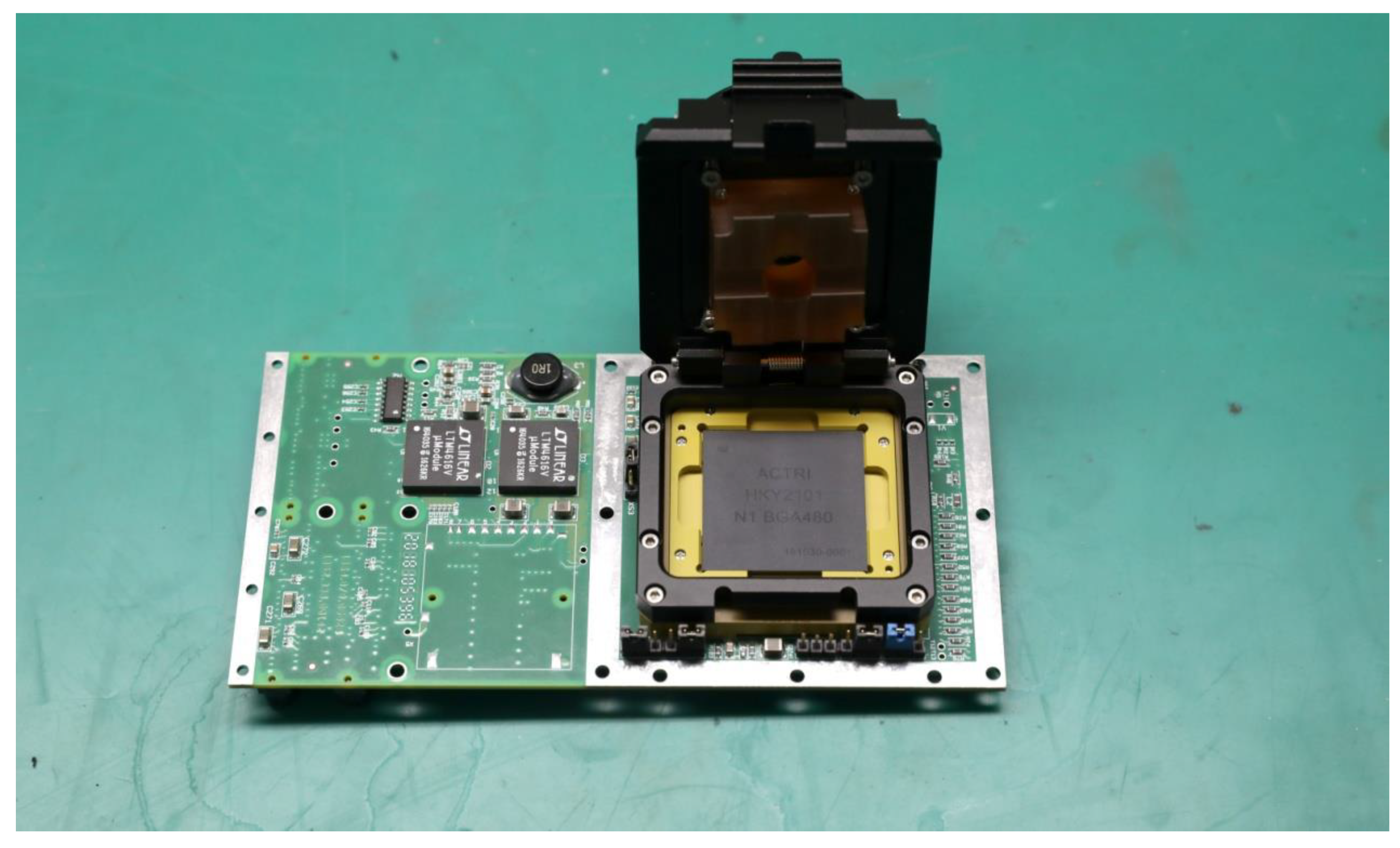
Test equipment and test circuit board for electrical function testing are developed. SIP chip and test board as shown in Figure 5. Using the test board to provide various power and clock, the SiP chip resets the signal and brings out its communication control interface for testing [8]. The specific functional test items include: CPU test, DDR3 test, UART test, RS422 communication test, CAN bus communication test, SPI interface test, I2C interface test, IO port test, ARINC429 communication test and 1553B bus communication test. Xilinx’s Vivado Design Suite environment is used for development testing. Programmable logic is used to build interface devices on the PL side [9]. The internal Zynq SoC builds are shown in Figure 6, including ARM_APU, UART_RS422 devices, GPIO devices, ARINC429 devices and 1553B device. Vivado’s SDK development tool is used to develop test software for testing. Target files are solidified into SiP SPI_FLASH. The function is normal after testing two SiP chips.

4.2. Analysis and Improvement of Chip Thermal Test

With the development of microelectronic technology, the heat flux density on the chip surface will be comparable to the heat flux density on the solar surface in the future. The heat dissipation technology of system in package (SiP) chips is becoming more and more important. The ambient temperature range of the chip was designed to be −40~85 °C initially. With the promotion of the application range, it was found that there is a high temperature application requirement of 100 °C. In order to expand the application scenario of the micro system chip and make it work reliably in a wider temperature range, it is necessary to test and analyze the heat dissipation characteristics of the micro system chip [10].
The test software used in the chip thermal test is the functional test software used in Section 4.1, including CPU test, DDR3 test, UART test, RS422 communication test, CAN and other functional interface tests. The resource utilization rate of the FPGA on the PL side is 55%. The SiP chip operates at 667 MHz ARM frequency and 1066 Mbps DDR3 speed.

4.2.1. Test Situation before Improvement

The temperature test box was used to perform detailed tests on the chip in a high-temperature environment [11]. It was found that when the ambient temperature reached 100 to 105 °C, the temperature of the Zynq die inside the SiP chip exceeded its maximum junction temperature of 125 °C. The temperature difference between ambient temperatures increases significantly in high-temperature environments. A range 100~105 °C is just the upper limit of high temperature for some industrial applications (such as mine monitoring). The heat dissipation of the SIP chip needs to be analyzed and improved in order to meet the high-temperature use requirements of 100 °C. The detailed test data are shown in Table 1. When the SiP chip works at ARM frequency 667 MHz and DDR3 rate 1066 Mbps, the measured value after 20 min of chip operation is recorded. The case temperature is used when the chip case and the external environment reach thermal equilibrium. The temperature measured by the instrument is the temperature of the heat-concentrated Zynq die inside the package. The temperature is measured using the internal AD temperature measurement circuit that comes with the Zynq chip.

4.2.2. Thermal Analysis

JEDEC’s general method for evaluating the thermal characteristics of IC silicon chips is to define the chip’s thermal resistance based on Equation (1).
TJTc = Rjc × P
TJ is the junction temperature of the chip. Tc is the case temperature of the outer surface of the package. P is the thermal power consumption of the device [12].
The SiP chip can fully release the heat to the environment through the substrate and the shell generally. However, natural cooling is not enough in some high-temperature environments. A thermally conductive material can be added inside the SiP chip to make the heat energy transfer to the outside of the chip faster and more effectively. This material can reduce the temperature difference between the internal die and the ambient temperature, and improve the maximum operating temperature allowable fot the SiP. The chip can reach thermal equilibrium as soon as possible.
The internal structure and thermal resistance model of SiP are shown in Figure 7. The housing package is a resin material. The internal chip is fixed on the substrate. The substrate is made of PCB. The internal chip and the housing are gas (nitrogen, etc.). The heat of the internal chip is first radiated into the gas, and then the gas is radiated out of the housing. This heat dissipation path is heat radiation. The lower part of the internal chip is thermally conductive. The heat is conducted to the outside through the substrate and the bottom solder ball.
The materials and thermal conductivity (W) are shown in Table 2. Try to choose materials with a high thermal conductivity for heat dissipation when selecting materials. The thermal expansion coefficients of different materials should not differ too much, because materials with different thermal expansion coefficients will generate stress during heating and cooling. It will also damage the wafer and cause reliability problems [13].
There is usually a temperature difference Δθ between the ambient temperature and the die temperature. If the temperature difference can be reduced, the die temperature will be relatively reduced at the same ambient temperature. In this way, the operating temperature level of the chip can be improved. Due to the low thermal conductivity of air and other gases, the thermal resistance of the system can be reduced to quickly transfer the heat of the die to the outside for reducing the temperature difference. The formula is
R = d/(Ka)
where: R is the thermal resistance; d is the thickness of the material; K is the thermal conductivity; a is the heat transfer area.

4.2.3. Thermal Improvement

High thermal conductive silver glue is a kind of chip adhesive developed especially for heat dissipation [15]. This glue which silver and resin particles are suspended in is a solvent carrier with a unique suspension. The thermal conductivity of this material is good. A thermally conductive silver glue is added above the Zynq die with the most concentrated heat dissipation in the SiP chip. The Zynq die is directly connected to the shell with the thermally conductive silver glue which reduces the thermal resistance and improves the chip’s heat dissipation capability. Two chips were repackaged. Under the same conditions, the high temperature test was performed again. The test results are shown in Table 3. The heat dissipation of the SiP chip at each temperature test point was obtained. With significant improvement, SiP chip has reached the high temperature requirement of 100~105 °C (junction temperature is less than 125 °C). The comparison of the heat dissipation before and after the improvement is shown in Figure 8.

4.3. Comparison with PCB Design

4.3.1. Comparison of Size and Power Consumption

In order to verify the circuit principle, a principle verification board (traditional PCB circuit board) was developed before the development of the SiP chip for comparative analysis. The relevant chips, such as Zynq SoC, were used instead of the dies for circuit testing and verification. In the SiP chip sample test, the SiP test board and the principle verification board were used for comparative test analysis. Compared with traditional PCB circuits, this aerospace SiP chip has a significant improvement in size/area and power consumption [16].
In terms of chip size, the thickness is ignored here since the thickness of each chip is 1mm to 2mm. Only the area occupied by the chip is considered. With traditional PCB circuit, Zynq SoC is 4.3 × 4.3 = 18.49 cm2, FLASH is 1.5 × 1 = 1.5 cm2, DDR3 is 2.5 × 1.5 = 3.75 cm2, 1553B transceiver is 1 × 1 = 1 cm2 and the total area is 24.74 cm2. With SiP chip, its area is 3.1 × 3.1 = 9.61 cm2. Regardless of the PCB wiring between separated chips, the volume/area is changed to 38.8% after being designed as a SiP chip. The volume reduction is more significant if wiring is considered.
In terms of power consumption, the principle verification board (same separation device) and the SiP test board run the same test software for test comparison in the case of the same peripheral circuit design. The main frequency is 667 MHz. The principle board verifies the whole board power consumption is 5 V × 0.649 A = 3.245 W. The entire board power consumption of the SiP test board is 5 V × 0.586 A = 2.93 W. The power consumption of the whole board is reduced by 90% after SiP design. The circuit connections between the dies are shortened. Signal integrity is improved. Line consumption and voltage drop are reduced. The signal termination resistors between Zynq SoC and DDR3 are removed to further reduce power consumption.

4.3.2. DDR3 Memory Test Comparison and Analysis

When the operating frequency of the system reaches 50 MHz and the board integration is higher, the interconnection and packaging of the circuit board components have an increasing influence on the whole electronic system. This will result in great distortion of the signal during transmission. For example, the clock signal or data signal on a high-speed circuit board generates overshoot, undershoot, delay, signal oscillation and distortion due to reflection, crosstalk, EMI or track collapse of the signal. This will affect the planned electronic system. The analysis of high-speed signal integrity has great practical significance [17].
Reflection means that when a signal propagates on a transmission line, a part of the signal is transmitted forward due to a discontinuous portion of the impedance, and another part of the signal returns along the original path [18]. Crosstalk refers to undesired voltage noise interference caused by electromagnetic coupling to adjacent transmission lines when signals are transmitted on the transmission line [19]. One of the most important issues with signal integrity is the reduction in signal crosstalk and reflection [20].
The interconnect between the Zynq SoC and DDR3 in this aerospace SiP chip is designed for high-speed signal integrity issues (DDR3 supports up to 1333 Mbps) [21]. The design is improved from the traditional PCB connection to the SiP package. The connection between the signals is shortened. The bonding wire process of Bonding Wire reduces the via holes, shortens the leads, enhances the impedance continuity of the signal transmission line and then reduces reflection. The chip is bonded to the leads with tightly coupled differential pair leads to reduce crosstalk [22]. The signal integrity of SiP is improved compared to traditional PCB, especially DDR3-related signals. After the SiP chip is used, the signal of the internal circuit interconnection cannot be detected. The oscilloscope signal test of the traditional circuit cannot be performed. Generally, the model simulation of the signal integrity of the circuit [23] has a certain gap with the actual measurement of the circuit. Read and write function tests do not intuitively reflect the quality of the signal [24], so a new signal integrity test method for integrated chips is needed. A DDR3 DQS signal-related read operation and write operation eye diagram pure software test method is used for comparative analysis.
An eye diagram is a method of expressing timing jitter and noise amplitude [25]. In the eye diagram, many data levels and edge transitions are superimposed in two-unit intervals (UI). The horizontal axis of the eye diagram represents time. The vertical axis represents the signal amplitude. An eye diagram is shown in Figure 9. The eye diagram contains a wealth of information. The impact of inter-symbol interference and noise can be observed from the eye diagram. The eye diagram reflects the overall characteristics of the digital signal and estimates the pros and cons of the system. The eye width introduced as a key metric from the eye diagram as a tool for evaluating the performance of signal interfaces. The larger the eye width, the better the signal quality [26].
The DQS signal is an important signal for DDR3. Differential data strobes (DQS and DQS#) are transmitted/received with data. Using the software method test, the Zynq SoC processor frequency is set to 667 MHz, the DDR3 frequency is set to 534 MHz, the SiP test board and the principle verification board use the same settings and the same DDR3 test software.
The read data eye width (per byte lane) is measured by shifting the read DQS position relative to the read data eye in both forward and backward directions, and finding the range in which a memory test is successful. The DQS offset is measured in 1/256 clock cycle units (256 units = one clock cycle). The default relative position of read DQS relative to the read data eye is a ¼ cycle shift (64 units). The test scans the DQS offset value from 64 upwards until a memory test fails on all lanes, and then from 60 downwards until a memory test fails on all lanes. Upon completion, the width and offset of the read data eye per byte lane is displayed. The state of all registers is then restored [27].
The write data eye width (per byte lane) is measured by shifting the write DQS position relative to the write data eye, and finding the range in which a memory test is successful. The DQS offset is measured in 1/256 clock cycle units (256 units = one clock cycle). The default relative position of write DQS relative to the write data eye is a ¼ cycle shift (64 units). The test scans the DQS offset value from a min to a max value (default 16–112) and marks the range in which a memory test is successful. Upon completion, the width and offset of the write data eye per byte lane is displayed.
Table 4 shows the DDR3 eye diagram test results of SiP and the principle verification board. Figure 10 shows the DQS original diagram test principle diagram of DDR3. With the SiP DD3 test and statistical analysis, read operation DQS average eye width is 89.84% and write operation DQS average eye width is 89.84%. With the principle verification board (traditional PCB design) DD3 test, read operation DQS average eye width is 88.28% and write operation DQS average eye width is 85.94%. The eye width of the SiP chip DDR3_DQS is significantly better than the principle verification board. The signal integrity of DDR3 is optimized and improved after changing the traditional PCB design to SiP packaged chips.

4.4. Aviation Computer Test and Comparison

4.4.1. Test Algorithm Selection

In the application of precision guided weapons and drones, multi-sensor data fusion is needed in guidance, navigation calculations and flight control calculations, such as infrared images, GPS/Beidou satellite positioning and inertial navigation. Here many integrated navigation algorithms and flight Control algorithm will involve the Kalman Filtering algorithm [28].
The purpose of the Kalman filter is to make the system state and the system truth value smaller and smaller by prediction in the course of time, and to make the most accurate filtering estimation of the state variables of the system [29]. Kalman filter recursion is divided into two processes: prediction and correction. The most commonly used information fusion method in navigation systems is to use Kalman filtering to perform data fusion on data from multiple sources. The standard Kalman filter can be directly used to obtain the optimal state estimation for a linear system with Gaussian-distributed noise.
Extended Kalman Filter (EKF) based on function linearization is an improved nonlinear filtering algorithm [30]. The principle of extended Kalman filter is that Taylor expansion of the point at the state estimation value retains only the first-order term, and then recursive using standard Kalman filter. The algorithm has strong practicability. The EKF algorithm mainly realizes the linearization of nonlinear systems by Taylor expansion of the nonlinear systems and ignoring higher-order terms.

4.4.2. Algorithm Design

Drone/UAV attitude control usually uses the quaternion method to update the attitude matrix in real time, and combines the sensors (gyroscope, accelerometer, magnetometer.) to calculate the output attitude [31]. The information fusion method based on Kalman filter algorithm improves the accuracy of system attitude measurement. Taking the heading measurement of the aircraft as an example, the EKF algorithm is used to calculate the heading angle of the aircraft for testing and comparing different computing platforms.
Let the geographic coordinate system be n and the carrier coordinate system be b. According to the rotation relationship of the coordinate system
n   =   T b n   ×   b
T b n is the rotation matrix of the carrier coordinate system b to the geographic coordinate system n. The use of the rotation matrix represents a large amount of calculation, which is difficult to calculate in real time. In engineering, quaternions are used to express posture information. The quaternion is a kind of higher-order complex number q ( q 0 + q 1 × i + q 2 × j + q 3 × k), which is commonly used in strapdown inertial navigation systems to represent a rotation transformation that rotates ( q 1 , q 2 , q 3 ) angles around an q 0 vector. Four elements can be converted to and from the rotation matrix representation.
T b n = [ q 0 2 + q 1 2 q 2 2 q 3 2 2 ( q 1 q 2 q 0 q 3 ) 2 ( q 1 q 3 + q 0 q 2 ) 2 ( q 1 q 2 + q 0 q 3 ) q 0 2 q 1 2 + q 2 2 q 3 2 2 ( q 3 q 2 q 0 q 1 ) 2 ( q 1 q 3 q 0 q 2 ) 2 ( q 2 q 3 q 0 q 1 ) q 0 2 q 1 2 q 2 2 + q 3 2 ]
Separate the continuous system and set the time interval for each algorithm update to T, the update law of the four-element method for discrete systems can be obtained
q n b ( t + T ) = ( I + 1 2 × S q n b n × T )   q n b ( t )
where q n b is the derivative of four elements and S q n b n is a rotation matrix related to angular velocity.
S q n b n = [ 0 ω x ω x 0 ω y ω z ω z ω y ω y ω z ω z ω y 0 ω x ω x 0 ]
The basic idea of the heading measurement system is to use the angular acceleration provided by the gyroscope and combine iterative integration calculations with the heading measurement system model. However, there will be a large drift due to the poor low frequency characteristics of the gyroscope. The accelerometer and the magnetometer correct the low frequency data to improve the static characteristics in the calculation of the heading measurement system. EKF is an algorithm widely used in the field of multi-sensor fusion. Its main algorithms are as follows.
Use the four element q = [ q 0 ,   q 1 ,   q 2 ,   q 3 ] T as the state quantity of the system. According to Equation (5), the average Gaussian noise is 0, and the prior prediction equation of the system is
q t ^ =   A t q t 1   =   ( I + 1 2 × S q n b n × T )   q t 1
Calculate the covariance of the current prior prediction based on the covariance of the previous moment
C t ^   =   A t C t 1 A t T + R t
where R t is the variance in the Gaussian noise introduced. The value of the accelerometer and magnetometer Z t = [ D a , D b ] T + R K is used as the observation of the system, where R K is the estimated error, then the measurement equation of the system is
D a = T b n [ 0 0 | g | ]
D b = T b n [ b x 0 b z ]
Among them, b x and b z are the values of the geomagnetic field in the world coordinate system. The specific values can be queried according to the local latitude and longitude. In order to obtain the Kalman gain, the Jacobian matrix of the measurement equation needs to be calculated
H K = z [ i ] q [ j ]
The Kalman gain K E and the four-element posterior estimate q t of the system can be obtained as
K E = C t ^ H K T ( H K C t ^ H K T + R K ) 1
q t   =   q t ^ + K E ( Z t H K q t ^ )
At this point, the optimal estimate of the pose at the current moment can be obtained. In order for the iterative algorithm to continue, the posterior estimate of the variance needs to be calculated
C t = ( I K E H K )   C t ^
When the error converges, a stable four-element value can be obtained and further converted. The angle is the heading angle of the system relative to the geographic coordinate system
y a w = t a n 1 ( 2 ( q 1 q 2 + q 0 q 3 ) q 0 2 + q 1 2 q 2 2 q 3 2 )

4.4.3. Aviation Computer Selection

In the test of aviation SiP microsystems, the EKF algorithm is used for comparison tests. The reference processor is STMicroelectronics’ main control chip STM32F407VGT6 used in a variety of commercial civilian drones of SZ DJI Technology Co., Ltd. Russia’s R-77 medium-range air-to-air missile uses a DSP processor [32]. A widely used DSP processor, TMS320F28335PGFA from Texas Instruments, will be selected as another comparative reference processor.

4.4.4. Comparison and Analysis of Test Results

The system uses a software–hardware cooperative method combining the advantages of the processor and programmable hardware. The PS (ARM) side implements the overall process control and the implementation of interactive control functions. Through the SPI bus and IMU sensors (gyro and accelerometer) and electronic compass Magnetometer needed to connect, the data acquisition and transmit to the PL terminal after data acquisition are completed. The EKF algorithm is run on the PL side. The parallel calculation is used to reduce the time required for the EKF algorithm. PS and PL use on-chip high-speed AXI bus to connect. The data throughput rate can reach 600 MB/s.
This is implemented using a high-level synthesis method (HLS). The algorithm flow which is completed in C language is converted into a hardware description language by Vivado HLS tools. The Vivado HLS tool provides an optimization strategy for loop unrolling, which can convert serial operations to parallel operations. Gauss–Jordan elimination method is used to solve the inverse matrix of the matrix. This algorithm has the highest time complexity and space complexity in the entire EKF algorithm. In order to speed up the calculation speed, the RAM_1P type storage space was opened for intermediate variables in advance. The algorithm for was accelerated in parallel.
The sensor board is fixed on a high-precision manual R-axis rotary table. The initial position of the sensor is adjusted to zero. The calculation period of the heading measurement system is 1 kHz. The initial conditions are q = [1, 0, 0, 0]T. The local gravity acceleration value is | g | = 9.79 m/s2. The local geomagnetic field strength is approximately B = [3.41 × 10⁻⁵ 0 3.57 × 10⁻⁵]T, and the covariance matrix R t of the system is
R t = [ 10 5 0 0 0 0 10 5 0 0 0 0 10 5 0 0 0 0 10 5 ]
The static performance of the system is tested first. The system stands for 120 s. In order to test the algorithm performance of this heading system, the turntable is rotated clockwise and counterclockwise. The output of the heading system is recorded. Repeating the experiment, the average and some measurements are taken. The list is shown in Table 5.
Test comparison results are shown in Table 6. It can be seen from the comparison that in the case of the smallest system design in which three types of aviation computers have external resources (RAM, FLASH), the micro-system chip has obvious advantages in computing performance with the integrated design of ARM + FPGA. It is also superior in volume/area design to the other two aviation computers. In terms of power consumption, the micro system chip is better than the TMS320F28335PGFA design, but it has a slightly higher power consumption than the STM32F407ZGT6, mainly due to the higher architecture of Cortex-A9 and the increase in resources such as FPGA and DDR3. With the development of battery technology and some specific application scenarios (for example, the flight time of missiles is short and limited), this increase in power consumption will not become a bottleneck for chip applications. The multiplication of its storage resources and computing resources is of the advantage which the other two aeronautical computers are incomparable with.
Table 7 shows the SiP test programmable logic resource usage. It can be seen from the FPGA resource usage in the table that the number of LUTs is insufficient to restrict the algorithm speed. This is because, when performing algorithm optimization, a large number of round robin operations will consume a large amount of LUT resources. However, the utilization rate of BRAM_18K in the system is not high. A large amount of reused data can be calculated and stored in advance in BRAM_18K to reduce the time of repeated calculations in order to further improve the solution speed.

5. Conclusions

This article introduces the design and implementation of an aerospace computer micro-system SiP chip. It explains and introduces its principle and simulation. It focuses on the SiP chip test including the comparison test between the SiP chip and the traditional PCB design and the thermal test. Analysis and comparison with other aviation computers are taken from testing. In terms of DDR3 signal integrity test comparison, a pure software eye diagram test method is used to verify the improvement in signal integrity. The focus is that the high-temperature range has been extended with the method of thermally conductive silver glue through thermal testing and analysis. The advantages of this SiP chip have been clarified by comparison with other aviation computer chips. Through analysis and comparison, it provides a reference for the future avionics SiP micro system design. Zynq SoC has software and hardware coordination and reconfigurable computing capabilities. It has many application advantages in graphic images, target tracking and flight control. The application development and promotion of this micro-system SiP chip will be a focus in the future. At the same time, the reliability improvement of this micro system SiP chip needs to be analyzed and studied.

Author Contributions

Methodology, Y.L. and W.H.; principle design, Y.C.; project administration, S.L.; test and writing, H.L.; algorithm and review, S.Z.; software, L.Z. All authors have read and agreed to the published version of the manuscript.

Funding

This research received no external funding.

Acknowledgments

The authors thank the support of Xi’an Aeronautics Computing Technique Research Institute, AVIC, China.

Conflicts of Interest

The authors declare no conflict of interest.

References

  1. Hu, Y.; Cai, J.; Cao, L.; Chen, L.; Liu, Z.; Shi, L.; Wang, Q. The research status and development trends of system in package (sip) technology. Equip. Electron. Prod. Manuf. 2012, 14, 1–6. [Google Scholar]
  2. Mounce, G.; Lyke, J.; Horan, S.; Doyle, R.; Some, R. Chiplet Based Approach for Heterogeneous Processing and Packaging Architectures. In Proceedings of the 2016 IEEE Aerospace Conference, Big Sky, MT, USA, 5–12 March 2016. [Google Scholar]
  3. Hao, W. Application of Sip Technology in Aerospace Products. Aerosp. Stand. 2013, 1, 30–33. [Google Scholar]
  4. Hang, C. Research of Missile-borne Computer Based on SiP. Dev. Innov. Mach. Electr. Prod. 2016, 29, 14–16. [Google Scholar]
  5. Ming, W.; Feng, W. SIP Packaging Technology. Electron. Packag. 2009, 2, 6. [Google Scholar]
  6. Pasca, V.; Anghel, L.; Nicolaidis, M.; Benabdenbi, M. Csl: Configurable fault tolerant serial links for inter-die communication in 3d systems. J. Electron. Test. 2016, 28, 137–150. [Google Scholar] [CrossRef]
  7. Tseng, H.L.; Huang, W.T.; Dai, J.C.; Chen, C.H.; Tan, S.Y. An evaluation eye diagram of a high-reliability fpga platform for high-resolution camera. Appl. Mech. Mater. 2015, 764, 1270–1274. [Google Scholar] [CrossRef]
  8. Lorena, A.; Mounir, B.; Alberto, B.; Marcello, T.; Ioana, V.E. Test and reliability in approximate computing. J. Electron. Test. 2018, 34, 375–387. [Google Scholar]
  9. Wang, H.; Bai, X.; Wu, Q. Multichannel High-Speed Data Caching System on FPGA for RAID Storage. In Proceedings of the International Conference in Communications, Signal Processing, and Systems, Dalian, China, 14–16 July 2018; Springer: Singapore, 2018. [Google Scholar]
  10. Meng, X. Temperature estimation of high temperature data acquisition multichip module for oil field apparatus. In Proceedings of the IEEE Intersociety Conference on Thermal and Thermomechanical Phenomena in Electronic Systems (ITherm), Las Vegas, NV, USA, 31 May–3 June 2016. [Google Scholar]
  11. Liu, L.; Jiang, P.; Zhao, X. The study of testing scenario for a SIP microcomputer. In Proceedings of the International Conference on Electronic Packaging Technology & High Density Packaging, Guilin, China, 13–16 August 2012; IEEE: Piscataway, NJ, USA, 2012. [Google Scholar]
  12. Canras, B.; Albarbar, A. A Technique for Mitigating Thermal Stress and Extending Life Cycle of Power Electronic Converters Used for Wind Turbines. Electronics 2015, 4, 947–968. [Google Scholar]
  13. Charles, H. Electronic Packaging and Interconnection Handbook; McGraw-Hill, Inc.: New York, NY, USA, 2004. [Google Scholar]
  14. Khan, A. Equilibrium Molecular Dynamics (MD) Simulation Study of Thermal Conductivity of Graphene Nanoribbon: A Comparative Study on MD Potentials. Electronics 2015, 4, 1109–1124. [Google Scholar] [CrossRef] [Green Version]
  15. Masahiro, I. Temperature Dependence of Electrical and Thermal Conductivities of an Epoxy-Based Isotropic Conductive Adhesive. J. Electron. Mater. 2008, 37, 462–468. [Google Scholar]
  16. Chen, M.S.; Chang, Y.C.; Chen, W.T.; Kuo, T.Y. Design and implementation of ultra-thin SiP modules. In Proceedings of the International Microsystems, Packaging, Assembly & Circuits Technology Conference, Taipei, Taiwan, 24–26 October 2012; IEEE: Piscataway, NJ, USA, 2012. [Google Scholar]
  17. Gao, L.; Wei, X.C.; Huang, Y.T.; Li, B.; Shu, Y.F. Analysis of near-field shielding effectiveness for the sip module. IEEE Trans. Electromagn. Compat. 2017, 60, 288–291. [Google Scholar] [CrossRef]
  18. Chastang, C.; Gautier, C.; Amedeo, A.; Costa, F. Crosstalk Analysis of Multigigabit Links on High Density Interconnects PCB using IBIS AMI Models. In Proceedings of the 2012 IEEE Electrical Design of Advanced Packaging and Systems Symposium (EDAPS), Taipei, Taiwan, 9–11 December 2012. [Google Scholar]
  19. Almalkawi, M.; Devabhaktuni, V. Far-End Crosstalk Reduction in PCB Interconnects Using Stepped Impedance Elements and Open-Circuited Stubs. Int. J. RF Microw. Comput.-Aided Eng. 2011, 21, 596–601. [Google Scholar] [CrossRef]
  20. Jin, S.; Han, L.; Xie, X. Signal integrity analysis of high-speed circuit board interconnecting DDR3 and FPGA. Mod. Electron. Tech. 2017, 40, 10–13. [Google Scholar]
  21. Jung, M.; Mathew, D.M.; Rheinlander, C.C.; Weis, C.; Wehn, N. A platform to analyze ddr3 dram’s power and retention time. IEEE Des. Test 2017, 34, 52–59. [Google Scholar] [CrossRef]
  22. Lee, J.-H. A Novel Meander Split Power/Ground Plane Reducing Crosstalk of Traces Crossing Over. Electronics 2019, 8, 1041. [Google Scholar] [CrossRef] [Green Version]
  23. Chuang, H.H.; Guo, W.D.; Lin, Y.H.; Chen, H.S.; Lu, Y.C.; Cheng, Y.S. Signal/power integrity modeling of high-speed memory modules using chip-package-board coanalysis. IEEE Trans. Electromagn. Compat. 2012, 52, 381–391. [Google Scholar] [CrossRef]
  24. Lai, Y.L.; Chiang, W.J. Characteristics of a system in a package with silver wires. Key Eng. Mater. 2015, 661, 121–127. [Google Scholar] [CrossRef]
  25. Odintsov, S.; Jutman, A.; Devadze, S.; Aleksejev, I. Embedded instrumentation toolbox for screening marginal defects and outliers for production. In Proceedings of the 2017 IEEE Autotestcon, Schaumburg, IL, USA, 9–15 September 2017; IEEE: Piscataway, NJ, USA, 2017. [Google Scholar]
  26. Yan, J. Realization of high speed link channel ber eye diagram based on der. Electron. Sci. Technol. 2016, 29, 30–33. [Google Scholar]
  27. Zynq Dram Diagnostics Test. Available online: www.xilinx.com (accessed on 15 January 2015).
  28. Chen, Y. Research on Attitude Measurement System Based on MEMS Inertial Devices. Master’s Thesis, North University of China, Taiyuan, China, 2019. [Google Scholar]
  29. Zakerzadeh, M.R.; Gerdefaramarzi, M.S.; Bozorg, M. Parameter estimation of an sma actuator model using an extended kalman filter. Mechatronics 2018, 50, 148–159. [Google Scholar]
  30. Barrios-dV, S.; Lopez-Franco, M.; Rios, J.D.; Arana-Daniel, N.; Lopez-Franco, C.; Alanis, A.Y. An Autonomous Path Controller in a System on Chip for Shrimp Robot. Electronics 2020, 9, 441. [Google Scholar] [CrossRef] [Green Version]
  31. Hao, Y. Indoor robots heading measurement system based on zynq platform. Microcontrollers Embed. Syst. 2017, 6, 22–27. [Google Scholar]
  32. Zhao, H. Analysis and Simulation of Integrated Guidance and Control System for R-77 Missile. Master’s Thesis, Southwest University of Science and Technology, Mianyang, China, 2012. [Google Scholar]
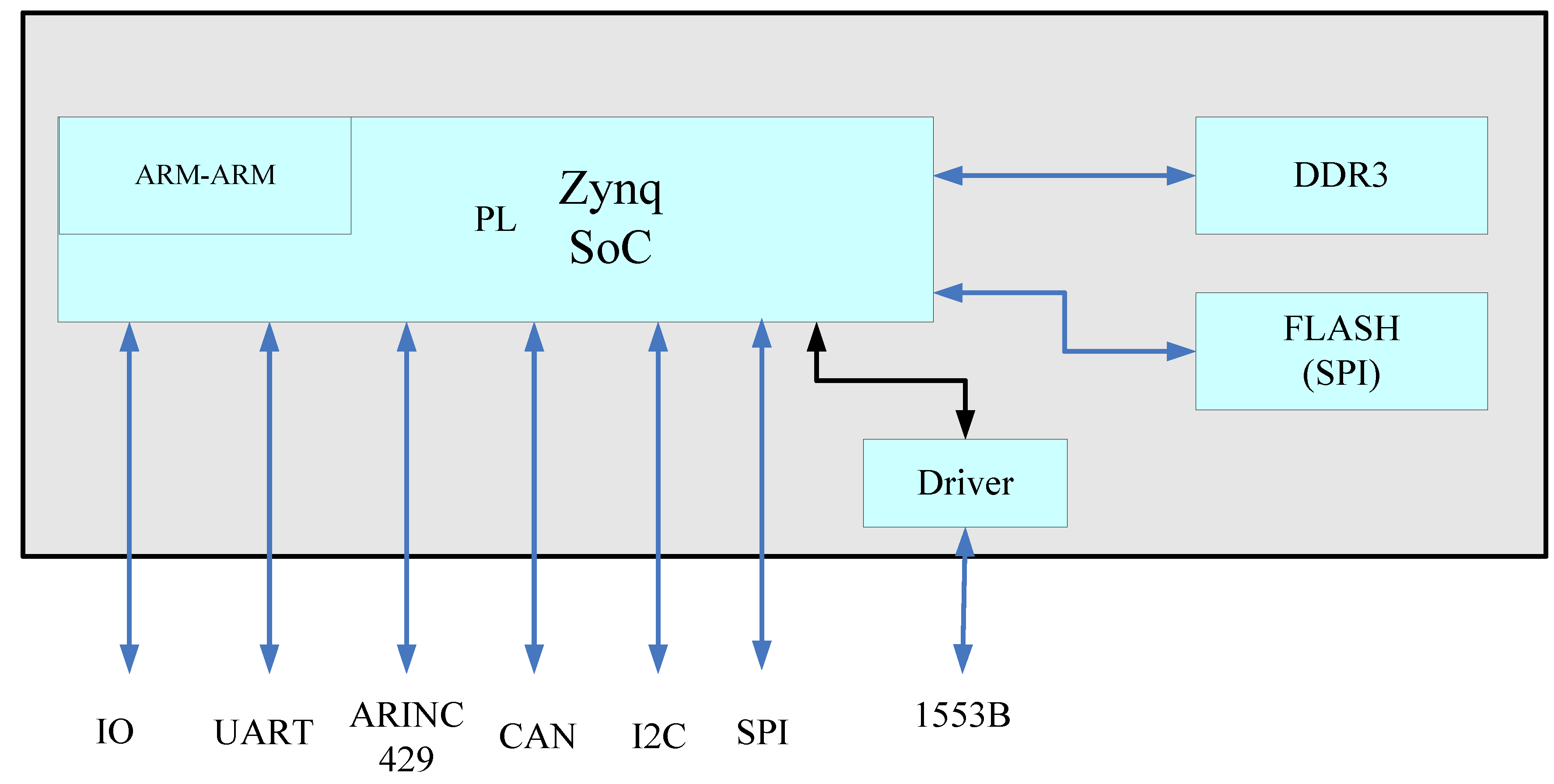
Figure 1. Internal structure of the system in package (SIP) chip.
Electronics 09 00766 g001
Figure 2. SiP internal die microphotographs. (a) SIP internal layout; (b) D9-Zynq die local photo; (c) D6-1553B driver die local photo; (d) D10-Flash die local photo; (e) D11-DDR3 die local photo.
Electronics 09 00766 g002
Figure 3. Voltage simulation result of the power supply DDR3 1.5 V is 1.49999~1.49737 V.
Electronics 09 00766 g003
Figure 4. Distribution of the chip under 200 g acceleration.
Electronics 09 00766 g004
Figure 5. Chip and test board picture.
Electronics 09 00766 g005
Figure 6. Zynq SoC internal construction diagram.
Electronics 09 00766 g006
Figure 7. SiP internal thermal resistance model.
Electronics 09 00766 g007
Figure 8. Comparison of heat dissipation before and after SiP chip’s improvement.
Electronics 09 00766 g008
Figure 9. Eye diagram principle.
Electronics 09 00766 g009
Figure 10. Eye diagram test schematic.
Electronics 09 00766 g010
Table 1. SiP chip (Zynq) high temperature test situation.
NO.Case TemperaturePower ConsumptionJunction Temperature
125 °C5 V, 0.235 A, 1.175 W35 °C
275 °C5 V, 0.265 A, 1.325 W90 °C
385 °C5 V, 0.268 A, 1.34 W101 °C
495 °C5 V, 0.278 A, 1.39 W113 °C
5100 °C5 V, 0.29 A, 1.45 W120 °C
6105 °C5 V, 0.294 A, 1.47 W128 °C
Table 2. SiP materials and corresponding thermal conductivity [14].
MaterialThermal Conductivity (W/mm · °C)
PCB0.013
Silicon0.146
Epoxy resin0.002
Thermal conductive silver adhesive0.0258
Gas (air)0.026 × 10⁻³
Table 3. High temperature test situation of SiP chip (Zynq) thermal improvement.
NO.Case TemperaturePower ConsumptionJunction Temperature
125 °C5 V, 0.234 A, 1.17 W31 °C
275 °C5 V, 0.260 A, 1.3 W84 °C
385 °C5 V, 0.264 A, 1.32 W96 °C
495 °C5 V, 0.277 A, 1.385 W106 °C
5100 °C5 V, 0.284 A, 1.42 W111 °C
6105 °C5 V, 0.292 A, 1.46 W117 °C
Table 4. DDR3_DQS read/write operation eye diagram test results.
Eye Result: (128 Unites = 1 Bit Time (Ideal Eye Width))
DescriptionLANE-0LANE-1LANE-2LANE-3
SIP_DDR3_ReadEYE[MIN-MAX][4, 120][4, 116][4, 120][4, 120]
EYE CENTER62/12860/12862/12862/128
EYE WIDTH90.62%87.5%90.62%90.62%
SIP_DDR3_WriteEYE[MIN-MAX][4, 120][8, 124][4, 120][8, 120]
EYE CENTER62/12866/12862/12864/128
EYE WIDTH90.62%90.62%90.62%87.50%
principle board_DDR3_ReadEYE[MIN-MAX][4, 120][8, 120][4, 116][8, 120]
EYE CENTER62/12864/12860/12864/128
EYE WIDTH90.62%87.50%87.50%87.50%
principle board_DDR3_WriteEYE[MIN-MAX][8, 116][8, 116][8, 120][8, 120]
EYE CENTER62/12862/12864/12864/128
EYE WIDTH84.38%84.38%87.50%87.50%
Table 5. Heading measurement record form.
Actual AngleSolution AngleErrorActual AngleSolution AngleError
−30°−30.685°0.68530°29.510°0.490
−90°−89.692°−0.30890°90.812°−0.812
−180°−178.24°−0.76180°181.571°−1.571
Table 6. Aviation computer comparison test form.
Test ChipArchitectureResources & ExtensionsFrequency/MHzTimePower/WArea/mm2
STM32F407ZGT6ARM Cortex-M4Flash 1MB+4MB
Sram 512KB+1MB
1683.413 ms0.50243 × 39
TMS320F28335PGFADSPFlash 512KB+4MB
Sram 68KB+1MB
1503.345 ms1.30749 × 42
SiP chipARM Cortex-A9
+FPGA
Flash 16MB
Ram 256KB
DDR3 128MB
667 (ARM)
50 (FPGA)
14.749 µs1.19531 × 31
Table 7. SIP test programmable logic resource usage.
ResourcesBRAM_18KDSP48EFlip-FlopsLUT
Total resources1208035,20017,600
Involved dosage426026,31513,552
Utilization/%357574.877