Abstract
Static Random-Access Memory (SRAM)-based Field Programmable Gate Arrays (FPGAs) are increasingly being used in many application domains due to their higher logic density and reconfiguration capabilities. However, with state-of-the-art FPGAs being manufactured in the latest technology nodes, reliability is becoming an important issue, particularly for safety-critical avionics, automotive, aerospace, industrial robotics, medical, and financial systems. Therefore, fault tolerant system design methodologies have become essential in the aforementioned application domains. The Isolation Design Flow (IDF) is one such design methodology that has promising prospects due to its ability to isolate logic design modules at the physical level for fault containment purposes. This paper proposes a methodology to evaluate the effectiveness of the IDF. To do so, reverse engineering is used to enable fault injection on the IDF designs with minimal changes in the bit-stream. This reduces the time needed to inject a fault significantly thus accelerating the evaluation process. Then this methodology is applied to a case study of a single-chip cryptography application on a ZynQ SoC. Specifically, an Advanced Encryption Standard (AES) Duplication With Comparison (DWC) design is physically isolated with IDF and subsequently subjected to frame-level Fault Injection (FI) in the configuration memory.
1. Introduction
Field Programmable Gate Arrays (FPGAs) revolutionized the field of embedded systems by providing the flexibility of reconfiguration in real time. FPGAs are considered to be a cost-effective replacement for ASICs in many applications as they provide benefits for users on two fronts: time and cost. First, they provide users with the flexibility to replace or amend their logic in the field, reducing the lengthy time involved in the process of ASIC manufacturing and development. Secondly, the cost incurred in the procurement of FPGAs is much less than developing an ASIC from scratch. However, the fact that state-of-the-art SRAM-based FPGAs are fabricated in the latest technology nodes, for example, Xilinx UltraScale+ in a 14 nm FinFET node, means that this class of semiconductor devices are vulnerable to radiation-induced failures, aging and electro-migration issues to name a few. Therefore, FPGAs also pose a challenge with respect to safety and security in mission-critical application areas and government/military sectors respectively; where the need for a reliable system is a must.
However, even these vulnerabilities have not hindered the widespread adoption of FPGAs in safety-critical fields such as avionics, aerospace, automotive, biomedical, financial and cryptographic systems where high reliability, high availability and high assurance are critical requirements. Systems, targeting these application domains are rigorously designed to achieve the required level of hardness-assurance according to industrial standards, for example, ISO26262 [1]. Vendors, also continuously spin-off design tools and methodologies to address the market needs for safety-critical domains. Information security standards for cryptographic modules or devices such as ISO27001 [2] and FIPS 140-2 [3] promote the idea of implementing well-defined, physically and logically separated data paths for information exchange on black (enciphered data) and red lines (plain data). The IDF itself is a part of the certified Xilinx IEC61508 toolchain [4]. IDF, in particular, achieves better system-level fault tolerance due to the module-level fault containment approach. For this purpose, it maps the logical interconnections of modules in a way that its physical level floor-planning on-chip avoids Single Point of Failures (SPOFs) which can make redundancy-based approaches such as Duplication With Comparison (DWC) and Triple Modular Redundancy (TMR) useless. Until now, designers for this market segment relied on multi-chip solutions for fault containment but the increased logic density and the industry-shift to processor-integrated FPGA fabrics, such as ZynQ SoCs demand on-chip isolation solutions.
To assess the effectiveness of the IDF, fault injection is needed to ensure that Single Point of Failures (SPOFs) are indeed avoided. Due to strict layout constraints imposed by IDF, use of Internal Configuration Access Port (ICAP) located in the Programmable Logic (PL) part of ZynQ, is not a good option as it can make isolation difficult to achieve. Therefore, fault injection has to be done over the Processor Configuration Access Port (PCAP) located in the Programmable System (PS) part of ZynQ. To the best of our knowledge, Xilinx does not provide any built-in EDA tools or library for frame-level fault injection over the PCAP interface as compared to AXI-ICAP. Therefore, existing fault injection methodologies for PCAP such as [5,6,7] require a large reconfiguration time and are thus slow. Furthermore, previous works that utilize PCAP rely on full bit-stream for fault injection purposes that have significant memory overhead. This paper introduces a testing and evaluation methodology for IDF designs that overcomes those limitations. This is achieved by reverse-engineering the partial bit-stream format for error injection so that full reconfiguration is not needed. To do so, a Partial Bit-stream Frame Template (PFT) is developed to enable run-time partial bit-stream generation and bit-flips inside DRAM memory. Then, the modified PFT is written back to the configuration memory using PCAP.
The proposed methodology was tested on a Xilinx ZynQ SoC housing an AES-based DWC Design Under Test (DUT) in the programmable logic portion. The DUT is carefully floor-planned with the strongest layout requirements of IDF with the overall goal of minimizing cross-domain errors or common mode failures. The results show that the proposed PFT-based methodology allows for much faster fault injections in comparison to existing schemes.
The paper is structured in the following manner: Section 1 provides the introduction and the motivation for the research, Section 2 covers the related work and background needed to follow the rest of the paper, Section 3 discusses the proposed methodology and Section 4 evaluates the methodology using a case study. Finally, Section 5 concludes the paper and provides some ideas for future work.
2. Background and Related Work
When creating an FPGA- or SoC-based design, the fundamental performance metrics for the designer have traditionally been area, time, and power. These constraints are what limit the implementation or impact of the cost in many systems. However, in order to create a robust and dependable design, there are other aspects that must be considered as well. In the following, other considerations that must be taken care of when developing reliable and dependable systems are summarized.
Security: Design security is a critical need in many industries, and classified and non-classified military applications. For this purpose, data encryption techniques are being used to mask actual data from the adversary. However, with the emergence of Side Channel Attacks (SCAs), researchers proposed and evaluated several designs, exposing their weaknesses. For example Lumbiarres et al. [8] created a method for achieving data security termed as “Faking countermeasure”. Their proposed solution is processing the unencrypted or plain-text data with the help of a false/fake key whose Electromagnetic (EM) wave emissions will mislead the attacker. The False key used for the purpose holds the KFALSE = KREAL ⨁ KMASK relationship with the original key. The additional operation needed at the end of each mix-column operation is exclusive-or of the false output with KREAL. This process adds a huge overhead for large chunks of data, with a primary focus on the AES design and thus cannot be extended to other cipher schemes. In the past, the National Security Agency (NSA) worked with Xilinx to secure Virtex-4 against attacks mentioned in [9]. The work performed was focused on evaluating isolation of basic building blocks on an FPGA; CLB’s and Global switch matrix (GSM) which is used to facilitate interconnect between CLB to CLB. The idea of a Fence; to provide a physical isolation was introduced in this paper. Xilinx further improved on this idea to create the IDF [10,11].
Reconfiguration: With the invention of dynamic partial reconfiguration (DPR), many applications can now share the same FPGA chip, carrying out their desired operations, side by side. DPR also opened doors to an entire new threat model, originally not present in traditional FPGAs. Zao et al. showed that side channel attacks on such environment are possible by using ring oscillators (RO), placing them in close proximity to secondary user’s space with the sole purpose of snooping data and information gathering/leaking [12]. Their RO based design acts as a power monitoring device which can relay information such as switching of bit(s) from 0 to 1 which can then be monitored to build a dictionary model upon which co-relation can be applied to extract the actual data. Moreover, such a design can be placed without using place and route constraints. Hence isolation (between users sharing the same FPGA space) to prevent Side Channel Attacks (SCA) is necessary.
Reconfiguration enabled FPGAs to gain a massive acceptance for big data analytics and parallel and distributed computational systems. Many companies employ solutions comprising an FPGA that can hold multi-tenants in cloud computing; as their general purpose computation machine. DPR is one of the key requirements to enable this form of cloud computing. DPR allows users to time multiplex FPGA resources enabling effective use of chip logic density. The reconfiguration time was thus reduced as the partial bit-stream size is fairly smaller than the whole bit-stream [13]. DPR allows a user design to be placed in static and dynamic parts. The dynamic or partial reconfigurable module can be arranged on chip in various configurations namely island style, slot style and grid style [14]. Each style has its own pros and cons. The island style is the simplest to implement but suffers from internal fragmentation resulting in a high percentage of resource wastage. Slot style configuration does not have fragmentation problems where a module can occupy resources as per its needs. Tiling of Reconfiguration Module (RM) region is a very complex task in which one has to keep in mind the placement of routes and their cross-over from static to dynamic regions. Thus, the DPR style to use depends on the user requirements and may vary from application to application. It may also consist of a model that is hybrid combining two or more styles.
Single Point of Failure (SPOF) Prevention: Embedded systems are designed and deployed every day to be used in every aspect of life ranging from submarines to handheld smart phones. If proper fault isolation and control mechanisms are not kept in mind during the design, the damages could be catastrophic as safety-critical systems are designed with the ultimate goal of being reliable. To avoid SPOF in systems, various solutions were provided. SPOF prevention can be put in place at (a) Internal components level (b) System level (Distributed Systems) (c) or a site wide level (Repetition). In the work provided in [15], SPOF prevention is introduced by building upon the existing Triple Module Redundancy (TMR) methods. In Reference [15], the authors propose the use of minority voters along with the majority voters to detect faults with better granularity. This technique can detect and help the user in correcting the fault by using the output of minority voters as a flag. Should the system fail to correct/detect the SPOF, it can minimize the damages if only the system is implemented upon isolated model; preferably at both physical and logical levels.
Heterogeneity: The first FPGAs developed were homogeneous devices. Presently, various functionalities are bundled down on a single chip. Isolated design helps achieve the best of FPGA heterogeneous nature, where a user can access and explore DSPs, BRAMs, and CLBs all in one place. In a heterogeneous system on chip (HRSoC) devices, user applications can be easily divided into various tasks. They can be either hardware accelerators-based which are built-into devices at pre-defined partition(s) or locations or can be implemented as a software task based on computing elements or CLBs. Gantel et al. in [16] made use of the heterogeneous nature of FPGA along with isolation to combine flexibility and reliability. Gantel used two isolated partitions (separately) that are identical to each other (resource wise) to ensure that the relocation process is achievable without physically damaging the chip (just as in IDF trusted routes are established to communicate various modules of a partition). A signal that is sink to two or more modules is split into different signals and passed through LUT resources to form trusted routes. Use of hard macros such as where ‘i, j’ are the valid XY coordinates of the chip, is done to constraint the synthesizer to a valid and desirable position. The isolation of designs ensured the error free relocation of modules in accessible dynamic partition space.
Fault Tolerance: The ability to control and withstand system failures is always a desired feature and is a requirement in government cryptographic systems, avionics, and functional safety electronics. This can be achieved by combining several systems that operate in parallel to ensure that the failure of some of them would not cause a global failure. This was proposed in [17], “A system composed of two or more redundant subsystems connected in parallel fashion, has a failure probability which is equals to the multiplicative product of the probabilities of each of the subsystems failing”. i.e., If the subsystems both had failure probability of , then the system made up of these subsystems has a reduced failure probability of = , which is many degrees lower in magnitude than individual subsystem failure rate [17]. However, this calculation assumes that probabilities of failure on each module are independent in nature i.e., the subsystems do not have a SPOF or common failure mode. This notion is the genesis of the isolation design flow. Fault-tolerance (FT) can be achieved by configuration scrubbing, floor-planning, module decomposition, reduced functionality modes, built-in self-tests (BIT) fault containment, failover and failback, redundant alarms, configuration memory error detection and error-recovery or correction mechanisms. Validation and verification of such FT methods can be realized using automated test procedures, diagnostic logging, design for test, and formal verification.
Xilinx Isolation Design Flow: Incorporating IDF in a user design has several advantages, such as; (1) IDF provides physical isolation between various modules, placed on a single-chip. (2) IDF helps in restricting error propagation between modules in an event of failure. (3) IDF allows ease of debugging and identification of the module causing a fault in an event of failure. (4) IDF allows enhanced failure protection by the use of trusting routing and well-defined logical boundary and separation of the modules. Although the advantages that IDF provides are important, it also has the following drawbacks: (1), IDF rules can be difficult to comprehend for novice users as sometime, they require FPGA placement and routing information that normal users may not possess. (2) IDF essentially limits users to design in a constrained environment (area wise) so larger designs might be difficult to fit onto chip along with IDF and lastly, incorporating IDF in a design, restricts the usage of dynamic partial reconfiguration once enabled. If a user wishes to implement IDF and DPR, side by side he has to do it with the help of third-party tools and API such as Go-Ahead [18] and BITMAN [19].
From this literature review, it is clear that modular isolation has many beneficial use cases. Many applications demand that the system works flawlessly, with an extreme degree of reliability. However, to verify that IDF is effective in avoiding or reducing SPOFs fault injection is needed. Current methodologies such as in [5,6,7,13,20] use PCAP to to emulate errors by placing ready-made partial bit-streams in an SD card to inject the errors. This results in a large injection time.
Other FI methods such as [21,22] make use of JTAG and ICAP interface respectively, to inject faults in DUT using external hardware whereas our proposed technique does not require any additional hardware to inject faults. Moreover, [21,22] also requires modification in DUT, such as insertion of Data Generator, Fault Generator, Error-detection, JTAG BSCAN modules and usage of external PCB hardware in order to emulate successful SEUs. Tobias et al. in [23] proposed usage of Soft-core processor in combination with ICAP, to inject and mitigate faults within 0.82 ms of its generation at the overhead of 32 KiB MicroBlaze memory. However, using a soft-core processor not only incurs a toll on PL resources (routing and logic) but may lead to other side-effects suggested by Villalta et al. in [5,24]. Author’s stresses that using ICAP for FI might be precarious and could easily lead to injection side-effects if a configuration bit that belongs to logic controlling ICAP is flipped and thus discourages the use of ICAP interface for FI.
In the following, a methodology that significantly accelerates fault injection is presented and evaluated on a single chip cryptographic application i.e., AES core mapped onto a ZynQ SoC.Proposed methodology uses PCAP for non-intrusive FI, saving precious PL resources and additional PCB hardware or OCD tool [25] in comparison to existing methodologies in [21,22,23].
3. Proposed Methodology
This section describes the methodology developed to accelerate error injection over the PCAP interface. The first part describes the Partial Frame Template (PFT) that is used to support injection at the frame level, the second part focuses on the challenges associated with using the PCAP interface and the third part presents the algorithm used for fault injection.
3.1. Partial Frame Template (PFT)
To introduce bit flips, we require to Read-Modify-Write the PL frames in a similar fashion as ICAP does. As previously stated, Xilinx neither allows module-level partial reconfiguration once IDF is enabled nor provides any library support for run-time partial bit-stream generation. To work around this problem, we studied the bit-stream structure of 7- Series FPGAs [26] and successfully reverse engineered the partial bit-stream structure. Using [26,27] and many generated bit-stream’s (full and partial) we devised a template, namely Partial Frame Template (PFT). The PFT contains all the necessary header and footer sequences (Refer Figure 1) that are required to target any 7-Series FPGA frame. PFT allowed us to generate our own partial FPGA configuration files without going through the extensive process of Vivado’s bit-stream generation, all in run-time. All the commands and frame data in the PFT were kept in SMAP x32 mode as we used PCAP to deliver configuration file to PL. Also, it is a requirement for PCAP that binary swapping of binary files must be disabled when targeting PCAP or MCAP [27]. It is to be noted here that PFT could only be loaded to the design, once the CRC check was disabled in original design file, as the partial bit-streams contain the CRC verification functionality, as a countermeasure to prevent faulty designs from loading onto PL which can cause permanent damage. Bit-stream CRC generation information is Xilinx proprietary and serves as a fail-safe. However, for our test and purposes it introduced an additional overhead thus, we bypassed it, saving time. After bypassing the CRC check, our PFT was able to load and configure any targeted PL frame, successfully. The contents of our proposed PFT are shown in Figure 1 for the reader’s understanding while Figure 2 shows the process to use our PFT to help readers, better follow the flow of our proposed methodology.
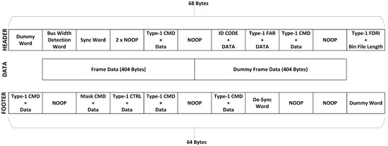
Figure 1.
Partial Frame Template (PFT) Structure.
Figure 2.
Partial Frame Template (PFT) Flow.
3.2. Challenges in PCAP
There are some limitations when performing read-back transfers that must be understood when performing PCAP-based PL read-back. When a PL read-back is requested, the returning data comes at a constant rate from the PL, whether or not the PCAP receiver FIFO is ready to receive incoming data. To prevent overflow of the receiver FIFO, the PCAP must transfer this data from the receiver FIFO to the destination memory via DMA over the PS AXI interconnect faster than the configuration module can fill up the receiver FIFO. The data rate can be calculated using the combination of PCAP clock rate and the PS AXI interconnect [28]. When performing continuous PCAP read backs, the DMA controller could hang and freeze the AXI bus, if too many frames are being read or if the frames are being read back too fast. This can be handled using two methods.
- Read fewer PL frames, preferably with long delays between each read back; in the order of milliseconds or more.
- Slow the PCAP clock frequency (default frequency = 100 MHz).
We slowed down the PCAP read-back clock to 50 MHz by writing to System Level Control Register-1 (SLCR). Another limitation of PCAP based PL read-back is that a single read-back request cannot be split over multiple DMA accesses. i.e., sending a command requesting 303 words of read-back data cannot be followed by a read of 101 words, then another read of 202 words. It must read all 303 words in one transfer. Thus, extreme care must be taken when specifying source and destination lengths of the data transfer.
Finally, due to hardware restrictions, all DMA transactions must be organized such that they do not cross a 4 KB boundary. Since PL read-backs request the number of desired frames plus one dummy frame for the frame buffer per transaction, the most data that the PS can request from the PL in a single transfer are 9 configuration frames + 1 dummy frame = 10 frames. It will be less than 10 frames if the transfer is reading data that crosses a row boundary. As 10 frames equate to 1010 words or 4040 bytes, which is just under the 4096 bytes (4 KB) boundary. Attempting to read more than 10 frames in a single transfer will result in a DMA transfer error. Each read-back performed on Zynq SoC requires two PCAP transfers processes, consisting of:
- Request the PL read-back data.
- Receive and store the incoming PCAP data.
While the PCAP has sufficient bandwidth capabilities to write bit-streams to the configuration without problems, the read back hardware is smaller i.e., the receiver FIFO is smaller than the transmit FIFO, 1 KB [20] and thus more limited. Our test setup, used to perform the PCAP-based PL read-backs and introduce the SEU’s to PL is shown in Figure 3 for the reader’s understanding.
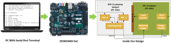
Figure 3.
Test Setup.
3.3. Fault Injection Process
Our proposed FI algorithm for replicating the effects of SEU’s in a controlled environment is presented in Algorithm 1. Step Write PFT shown in Algorithm 1 entails the following:
- During the initialization stage of our design we upload the complete PFT at a specific location in DRAM i.e., 0 × 200,000 with FAR address and data initially set to zero.
- A read back using PCAP is performed for the desired PL frame, which is saved as a golden frame (until all 3232 bits of a frame are checked).
- We update the FAR address location in PFT, present in DRAM at 0 × 20002C. It is to be noted here that only the FAR address location is being modified in the header section of PFT.
- We now pick the golden frame read in 2, modify one bit and write the modified (erroneous) frame, in data section of our PFT present in DRAM from 0 × 200044–0 × 2000A9 (101 Words).
- Hence, the run time partial bit-stream is generated.
- We load this newly generated, run time partial bit-stream to PL via PCAP.
- At this point, our algorithm checks, whether or not we have reached the last partial bit-stream (LPB), if so, it terminates, otherwise we go back to step 2 and continue, where LPB is calculated as follow:
LPB = (Total FI Target frames) × (Number of Words in a frame) × (Number of bits in a word)
Hence, for 15 FI Targeted frames that will be used in the next section the total run-time generated partial bit-streams were:
LPB = 15 × 101 × 32 = 48,480
| Algorithm 1: Fault Injection Algorithm |
 |
4. Evaluation
This section evaluates the proposed methodology using a single-chip cryptography application as a case study. Specifically, an Advanced Encryption Standard (AES) Duplication With Comparison (DWC) design is used.
Xilinx provided IDF comes in two flavors: (1) IDF for Plan-ahead and (2) IDF for Vivado. The rules and key concepts of IDF defined for both do not vary, but the approach for its use and isolation verification method varies significantly i.e., IVT for (1) and VIV for (2) respectively. We chose to work with Vivado’s IDF because the other tool has become obsolete. For this purpose, a design has been implemented on Zynq SoC, “Zed-Board” that conforms to the rules specified by the IDF. The verification of all IDF Design Rule Checks (DRCs) were performed using the Vivado’s Isolation Verifier (VIV) to qualify the implemented design for IDF. Xilinx has also provided an application note for user’s ease of understanding of IDF rules and regulations [11]. The first part of the design was implemented using Processing System (PS) part of the Zynq SoC whereas the second part of the design was realized on the Progammable Logic (PL) part of the Zynq SoC. We built our own custom AES-256 [29] cryptographic Verilog core based on a similar hierarchy presented in [11] using Vivado 2018.2 (the latest stable version available at the time of this study). The block diagram of our implementation is presented in Figure 4. The design was realized using IP Integrator (IPI) feature of Vivado 2018.2. Each module, shown in Figure 4, lies in its own separate hierarchy with each module partitioned and mapped to a well-defined location.
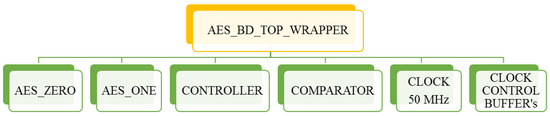
Figure 4.
AES-256-based IDF Design Hierarchy.
These constraints were placed using Vivado’s XDC file to keep track of all routing and logic track placements. (FI Target) and (Golden Copy) are DWC design under test. Each AES module has 4 input signals; clock (50 MHz), active low reset signal, a clock enable (realized using clock buffer) and a start signal to initiate the encryption process. Clock and reset signals were provided by Zynq processing system (PL-Fabric Clock and Clock Resets), whereas the clock enable, start signal for these modules were controlled and provided externally via PS MIO (controlled programmatically from PS). There exists another output signal Match, routed to PS via MIO which is used to monitor and record the output of the modules on each iteration. Logic use of our design (programmable logic) is summarized in Table 1 for reader’s reference.

Table 1.
Logic Use Summary for IDF and Non-IDF Designs.
The Hardware–Software co-design technique was used to test the effectiveness of the IDF in the presence of faults and SEUs. The Fault Injection (FI) logic was implemented completely on ZynQ PS section for the purpose of making it non-intrusive. Faults were introduced to the HW evaluation part using the PCAP interface present on ZynQ SoC. The ZynQ SoC contains a new configuration interface known as the Processor Configuration Access Port (PCAP). The PCAP is the gateway for the PS to access the PL configuration memory. PCAP includes a Direct Memory Access (DMA) controller, an AXI bus interface to communicate on the PS AXI interconnect, and a pair of FIFOs (transmit and receive) [28]. This interface essentially grants the PS an easy access to perform configuration operations (such as programming a bit-stream) to the PL. The PCAP is somewhat unique, among configuration interfaces as it does not require a specialized cable or dedicated I/O pins (unlike JTAG or Select-MAP). Instead, the PCAP is accessible to the user, purely through software by using dedicated memory-mapped registers. We used PCAP to read PL frames, perform FI on the frame and load the erroneous frame back to PL to emulate the SEUs caused by radiation.
The evaluation process of IDF begins by uploading a Partial Frame Template (PFT) in PS DRAM containing all the necessary, Synchronization header, Frame Data, Dummy Frame Data and De-Synchronization footer sequence for 7-series FPGA [26]. After PFT is loaded, a frame is read back using PCAP and written to the same Frame Address register (FAR) location with a difference being that 1-bit is now flipped from its original state to emulate the effects of an SEU in a controlled environment. Prior to this process, the clock of the HW evaluation part is stopped to better observe the results of FI introduced in the system.
Once the erroneous PFT insertion is complete, the clock is restored to the HW evaluation part and the DWC AES-256 cores are given the start signal to begin the encryption process. Outputs of both AES cores (Golden and FI target) are fed to a comparator for matching which generates a Match signal if the results of both AES cores differ. The Match signal is read back to PS via external MIO and its occurrences are logged for each iteration. After logging the Match signal, the FI originally performed is removed and then FI is performed on the next bit of a current FAR. The 7-Series FPGAs frame consists of 101 words. Each word is 32-bits wide. Hence, the test input space for a frame wide SEU is calculated as 101 × 32 = 3232. For replicating the SEU in one frame of 7-Series FPGAs, the aforementioned process was run repeatedly for 3232 iterations over various frames (FAR’s) to better assess the effectiveness of IDF in the presence of FI.
The layout of our IDF-based designs, as shown in Figure 5, depicts the placement of isolated modules, FI target for our evaluation methodology and IDF-based fences around the various resource such as FIFO, BRAM and IOB Buffers.To investigate and comprehend the effectiveness of IDF, two designs were compared; one with all the IDF and placement constraints and another without IDF constraints (with the same placement constraints as the first design). The FI algorithm mentioned in the previous section was run repeatedly, in several iterations for both designs, injecting non-intrusive SEUs and the effects of these SEUs were recorded. The results were obtained by performing FI in several PL locations which are marked in Figure 5 for the reader’s visualization, along with the areas where the HW evaluation candidate AES_ Zero and AES_ One were located on ZynQ SoC Chip. Some of the results collected during this analysis are also tabulated in Table 2 where the areas that correspond to the interconnections of the two AES modules are highlighted in boldface. It can be seen that those areas such as 43B and 25F showed a higher concentration of errors in the Non-IDF design because this is where the logic boundaries (AES _ Zero and Comparator module horizontally and AES _One vertically) were present. Critical routing bits of these modules were located without any isolation between them and our introduced SEUs resulted in a disconnection between logic. However, once the IDF was enabled and fences were placed around this area, the number of errors reduced significantly in those areas, as IDF ensured the placement of critical routing information with-in the specified isolated, p-block regions. Areas 1A-22L were mostly vacant slices, with minimum or no logic present, hence FI on these locations did not produce many noticeable errors.
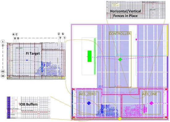
Figure 5.
IDF Design, Implementation view with Controller marked in Green, AES_Zero marked in Blue, AES_One in Purple and Comparator marked in Yellow.
Table 2.
Error Rate Comparison for IDF and Non-IDF-Based Design (Annotated Markers in Figure 5).
From Table 2, it is evident that once the IDF was incorporated in our design (and trusted routing was enabled by Vivado), the error rate reduced drastically for the areas that correspond to the interconnections of the two modules. However, the elimination of these errors that could lead to SPOFs is not cost-free. The trusted routing and design fence that were incorporated in the design reserved resources with-in the ZynQ SoC chip and these resources were thus essentially unavailable to our design.
Table 3 summarizes the total Zynq SoC resources available to our design in IDF and Non-IDF design environment along with the total percentage use of resources reserved by IDF by employing fences, trusted routing and modular isolations. By carefully analyzing the resources use obtained in Table 3, we observed the following: (1) When IDF is enabled for a design, Vivado’s synthesizer reserves some resources from the chip and prohibits its usage in user design thus, creating a physical boundary; a separation between each isolated module which restricts the propagation of error in an event of system failure. (2) The size of resources that are effectively marked unusable, as a result of enabling IDF in a design varies and depends on (a) Number of isolated modules (b) Height of fence applied (c) Width of fence applied (d) Complexity of logic being implemented in terms of slice and primitive use (e) Number of global clocking components (f) Route/signals exempt from isolation. The resource overhead that IDF incurs thus, may vary from design to design. However, the resource overhead in comparison to its effectiveness against fault containment over-weighs itself.
Table 3.
IDF Resource Utilization Overview.
Using Vivado design power estimator we collected the power consumption data for our IDF and Non-IDF design which is presented in Table 4. It can be seen that the power consumption is almost the same in both cases and the use of IDF seems to have little impact.
Table 4.
Power Consumption of IDF and Non-IDF Designs.
The timing summary of our implemented modules is presented in Table 5. In this case, there is an increase of the maximum frequency of operation when using the IDF but the difference is not large.
Table 5.
Timing Constraints Summary in nanoseconds (ns).
Finally, let us discuss the benefits in terms of fault injection acceleration provided by the proposed methodology. As discussed before this acceleration is the main objective of the proposed methodology. There are two main components in the time needed for fault injection that depends on the methodology. The first one is the generation of the bit-streams used for the fault injection and the second is the time needed to download those bit-streams to the FPGA to test the error.
For the first component, our novel, one frame PFT is generated in real time in comparison to the partial bit-streams generated by Xilinx tools. It is to be noted here that the average time to generate a partial bit-stream taken by Xilinx Vivado Design Suite 2018.2 on our average PC with Intel(R) Core (TM) i5-4500M Quad core CPU @ 2.50 GHz and 8.0 GB RAM was roughly 10 minutes whereas our PFT was generated in 0.2 s thus achieving a 3000× reduction in the time needed. It must be noted that the proposed methodology also eliminates the need to store the partial bit-streams used for fault injection. Table 6 gives the sizes and generation times of the different options for the for the XC7020 bit-stream.
Table 6.
Generation Time Comparison for XC7020 Bit-stream.
For the second component, the time needed to download the bit-stream to the device, the size of the Zynq XC7Z020 All Programmable SoC full bit-stream is 4,045,564 bytes and its configuration time using PCAP in a standalone, bare-metal environment is measured to be 32 ms in [30]. As the size of the partial bit-stream is smaller than the full bit-stream, it requires less configuration time, approximately 1 ms. However, Xilinx tools cannot generate a partial bit-stream which targets and configures only one frame [5]. This is where the proposed PFT provides a significant advantage by enabling the single frame modification that can be done in less than 0.015 ms. The times are summarized in Table 7 and corresponds to an average time, measured between the beginning and end of DevC DMA transfer function call with PCAP clocked at 100 MHz whereas, for our proposed PFT, PCAP was clocked at 50 MHz. It can be seen that the proposed methodology reduces the time needed to download the bit-stream that injects the failure by a factor of approximately 67× compared to the previous scheme that performs fault injection by downloading larger partial bit-streams over the PCAP interface [5,6,7,13].
Table 7.
Configuration Time Comparison for XC7020 Bit-stream.
As a summary, the results discussed show that the proposed methodology is able to provide very significant reductions in both the time needed to generate the partial bit-streams needed for fault injection and also in downloading those to the configuration memory of the FPGA.
5. Conclusions
This paper proposed an evaluation methodology for validating and verifying the effectiveness for Xilinx Isolation Design Flow (IDF). The proposed methodology addresses the problem of non-intrusiveness of fault injection infrastructure and develops a reverse-engineering-based approach to enable Processor Configuration Access Port (PCAP)-based frame-level bit-flip manipulation. The fault injection infrastructure is not only non-intrusive but does not requires any resource in the programmable logic portion and is entirely contained in the programmable system of ZynQ SoC. The proposed scheme enables a very significant acceleration of the fault injection reducing the time needed to generate a run-time partial bit-stream and downloading it to the FPGA by a factor of more than 67×. As future work, we would like to explore how the IDF rules can be utilized to reduce cross-domain errors in FPGA-based TMR designs.
Author Contributions
A.A.M. and A.U. contributed to the design and implementation of the proposed evaluation methodology. A.A.M., A.U., A.Z., A.Q., S.K.K., and P.R. participated in the writing and revision of the paper. All authors contributed to the analysis of the results and comparisons with previous schemes. All authors have read and agreed to the published version of the manuscript.
Funding
This research received no external funding.
Conflicts of Interest
The authors declare no conflict of interest.
References
- Schätz, B.; Voss, S.; Zverlov, S. Automating design-space exploration: Optimal deployment of automotive SW-components in an ISO26262 context. In Proceedings of the 52nd Annual Design Automation Conference, San Francisco, CA, USA, 8–12 June 2015; pp. 1–6. [Google Scholar]
- Disterer, G. ISO/IEC 27000, 27001 and 27002 for information security management. J. Inf. Secur. 2013, 4, 92–100. [Google Scholar] [CrossRef]
- Caddy, T. FIPS 140-2. 2005. Available online: https://csrc.nist.gov/publications/detail/fips/140/2/final (accessed on 14 May 2020).
- Bell, R. Introduction to IEC 61508. ACM International Conference Proceeding Series. 2006, Volume 162, pp. 3–12. Available online: https://www.semanticscholar.org/paper/Introduction-to-IEC-61508-Bootle/1fa95e2147da7d27cc9a25166d43c9ad6e17ac2e (accessed on 14 May 2020).
- Villalta, I.; Bidarte, U.; Santos, G.; Matallana, A.; Jiménez, J. Fault injection system for SEU emulation in Zynq SoCs. In Proceedings of the Design of Circuits and Integrated Systems, Madrid, Spain, 26–28 November 2014; pp. 1–6. [Google Scholar]
- Stoddard, A.; Gruwell, A.; Zabriskie, P.; Wirthlin, M. High-speed PCAP configuration scrubbing on Zynq-7000 all programmable socs. In Proceedings of the 26th International Conference on Field Programmable Logic and Applications (FPL), Lausanne, Switzerland, 29 August–2 September 2016; pp. 1–8. [Google Scholar]
- Villalta, I.; Bidarte, U.; Gómez-Cornejo, J.; Jiménez, J.; Lázaro, J. SEU emulation in industrial SoCs combining microprocessor and FPGA. Reliab. Eng. Syst. Saf. 2018, 170, 53–63. [Google Scholar] [CrossRef]
- Lumbiarres-López, R.; López-García, M.; Cantó-Navarro, E. Hardware architecture implemented on FPGA for protecting cryptographic keys against side-channel attacks. IEEE Trans. Depend. Secur. Comput. 2016, 15, 898–905. [Google Scholar] [CrossRef]
- McLean, M.; Moore, J. FPGA-based single chip cryptographic solution. In Military Embedded Systems; 2007; pp. 34–37. Available online: http://mil-embedded.com/pdfs/NSA.Mar07.pdf (accessed on 14 May 2020).
- Xilinx. Xilinx 7 Series Isolation Design Flow Lab Using ISE Design Suite 14.4; Xilinx Inc.: San Hose, CA, USA, 2013; Volume 11, pp. 1–102. [Google Scholar]
- Hallett, E. Isolation Design Flow for Xilinx 7 Series FPGAs or Zynq-7000 AP SoCs (Vivado Tools), v1; Xilinx Inc.: San Hose, CA, USA, 2016; Volume 9. [Google Scholar]
- Zhao, M.; Suh, G.E. FPGA-based remote power side-channel attacks. In Proceedings of the IEEE Symposium on Security and Privacy (SP), San Francisco, CA, USA, 20–24 May 2018; pp. 229–244. [Google Scholar]
- Vipin, K.; Fahmy, S.A. FPGA dynamic and partial reconfiguration: A survey of architectures, methods, and applications. In ACM Computing Surveys (CSUR); ACM: New York, NY, USA, 2018; Volume 51, pp. 1–39. [Google Scholar]
- Voros, N.; Huebner, M.; Keramidas, G.; Goehringer, D.; Antonopoulos, C.; Diniz, P.C. Applied Reconfigurable Computing. Architectures, Tools, and Applications. In Proceedings of the 14th International Symposium, ARC 2018, Santorini, Greece, 2–4 May 2018; Springer: Cham, Switzerland, 2018; Volume 10824. [Google Scholar]
- Sterpone, L.; Ullah, A. On the optimal reconfiguration times for TMR circuits on SRAM based FPGAs. In Proceedings of the NASA/ESA Conference on Adaptive Hardware and Systems (AHS-2013), Torino, Italy, 24–27 June 2013; pp. 9–14. [Google Scholar]
- Gantel, L.; Benkhelifa, M.E.A.; Lemonnier, F.; Verdier, F. Module relocation in heterogeneous reconfigurable systems-on-chip using the xilinx isolation design flow. In Proceedings of the International Conference on Reconfigurable Computing and FPGAs, Cancun, Mexico, 5–7 December 2012; pp. 1–6. [Google Scholar]
- Von Neumann, J. Probabilistic logics and the synthesis of reliable organisms from unreliable components. Autom. Stud. 1956, 34, 43–98. [Google Scholar]
- Beckhoff, C.; Koch, D.; Torresen, J. Go ahead: A partial reconfiguration framework. In Proceedings of the IEEE 20th International Symposium on Field-Programmable Custom Computing Machines, Toronto, ON, Canada, 29 April–1 May 2012; pp. 37–44. [Google Scholar]
- Pham, K.D.; Horta, E.; Koch, D. BITMAN: A tool and API for FPGA bitstream manipulations. In Proceedings of the Design, Automation & Test in Europe Conference & Exhibition (DATE), Lausanne, Switzerland, 27–31 March 2017; pp. 894–897. [Google Scholar]
- Stoddard, A.G. Configuration Scrubbing Architectures for High-Reliability FPGA Systems. Master’s Thesis, Brigham Young University, Provo, UT, USA, 2015. [Google Scholar]
- Thurlow, C.; Rowberry, H.; Wirthlin, M. TURTLE: A Low-Cost Fault Injection Platform for SRAM-based FPGAs. In Proceedings of the International Conference on ReConFigurable Computing and FPGAs (ReConFig), Cancun, Mexico, 9–11 December 2019; pp. 1–8. [Google Scholar]
- Di Carlo, S.; Prinetto, P.; Rolfo, D.; Trotta, P. A fault injection methodology and infrastructure for fast single event upsets emulation on Xilinx SRAM-based FPGAs. In Proceedings of the IEEE International Symposium on Defect and Fault Tolerance in VLSI and Nanotechnology Systems (DFT), Amsterdam, The Netherlands, 1–3 October 2014; pp. 159–164. [Google Scholar]
- Dörr, T.; Sandmann, T.; Schade, F.; Bapp, F.K.; Becker, J. Leveraging the Partial Reconfiguration Capability of FPGAs for Processor-Based Fail-Operational Systems. In Proceedings of the International Symposium on Applied Reconfigurable Computing, Darmstadt, Germany, 9–11 April 2019; Springer: Cham, Switzerland, 2019; pp. 96–111. [Google Scholar]
- Villalta, I.; Bidarte, U.; Gomez-Cornejo, J.; Lázaro, J.; Astarloa, A. Estimating the SEU failure rate of designs implemented in FPGAs in presence of MCUs. Microelectron. Reliab. 2017, 78, 85–92. [Google Scholar] [CrossRef]
- Portela-Garcia, M.; Lopez-Ongil, C.; Valderas, M.G.; Entrena, L. Fault injection in modern microprocessors using on-chip debugging infrastructures. IEEE Transa. Depend. Secur. Comput. 2010, 8, 308–314. [Google Scholar] [CrossRef]
- Series FPGAs Configuration. UG470, v1 7. pp. 1–176. Available online: https://www.xilinx.com/support/documentation/user_guides/ug470_7Series_Config.pdf (accessed on 14 May 2020).
- Technical Report UG909. In Reconfigurable Computing. Architectures, Tools, and Applications; Xilinx: San Hose, CA, USA, 2018; Available online: https://www.xilinx.com/support/documentation/sw_manuals/xilinx2017_1/ug909-vivado-partial-reconfiguration.pdf (accessed on 14 May 2020).
- Xilinx Inc. Zynq-7000 All Programmable SoC; Xilinx: San Hose, CA, USA, 2012. [Google Scholar]
- 197, Advanced Encryption Standard (AES), National Institute of Standards and Technology, US Department of Commerce. November 2001. Available online: https://csrc.nist.gov/publications/detail/fips/197/final (accessed on 14 May 2020).
- Kohn, C. Partial reconfiguration of a hardware accelerator on zynq-7000 all programmable soc devices. In Xilinx, XAPP1159 (v1. 0); Xilinx: San Hose, CA, USA, 2013. [Google Scholar]


© 2020 by the authors. Licensee MDPI, Basel, Switzerland. This article is an open access article distributed under the terms and conditions of the Creative Commons Attribution (CC BY) license (http://creativecommons.org/licenses/by/4.0/).