Letter

Compact Medium Voltage DC/DC Converter Using Series-Connected Power Devices

1
State Key Laboratory of Marine Geology, Tongji University, Shanghai 200092, China
2
School of Ocean and Earth Science, Tongji University, Shanghai 200092, China
3
Center for Marine Science and Technology, Tongji University, Shanghai 200092, China
*
Author to whom correspondence should be addressed.
Electronics 2020, 9(6), 1024; https://doi.org/10.3390/electronics9061024
Submission received: 4 June 2020 / Revised: 15 June 2020 / Accepted: 18 June 2020 / Published: 21 June 2020
(This article belongs to the Section Power Electronics)

Abstract

:
Medium voltage (MV) DC/DC converters are key equipment for interconnection between DC power lines with different voltage levels in MVDC grids. The Input-series-output-parallel (ISOP) modular MV DC/DC converter is feasible to realize MV to low voltage (LV) conversion. However, a large number of LV modules in the converter may reduce the reliability and increase the complexity. This letter proposes a phase-shifted full-bridge MV DC/DC converter using series-connected power devices as switching modules. The converter is of low cost, simple structure, compact volume, and high reliability because these switching modules require only one external isolated driver circuit and very few components to achieve voltage sharing among series-connected power devices. The operation principle of the switching modules is analyzed, and the simulation and experimental results validate the feasibility of the converter design.

1. Introduction

Recently, with the development of distributed renewable energy power systems, medium voltage (MV) DC grids have gained growing interest. The MV DC/DC converters that step down thousands of volts to hundreds of volts are key equipment in MVDC grids [1]. The undersea power systems of cabled seafloor observatories or distant subsea oil and gas fields are MVDC grids to power underwater equipment using medium voltages of the order of thousands of volts [2,3]. MV DC/DC converters for subsea MVDC grids require compact volume, high reliability, and high power density.
The bottleneck of MV DC/DC converters is that mature semiconductor power devices cannot meet the voltage and power needs. There are two approaches to solve the problem. One is modular converters with input-series output-parallel (ISOP) connected low voltage (LV) input power electronics building blocks (PEBBs) [4,5,6,7,8,9,10,11,12,13]. The other is to develop new semiconductor power devices with high blocking voltages or connect power devices in series to reach high blocking voltages, based on conventional converter topologies [14].
Although the ISOP modular converters have some advantages, e.g., LV component availability and possibly higher efficiency [8], a large number of PEBBs will lead to a complex control system for input voltage sharing and output current sharing. Poor input voltage sharing and output current sharing can greatly reduce the stability of modular converters [6,9,10,11,12]. Moreover, there are a large number of semiconductor power devices in modular converters, so a large number of isolated driver circuits are required, which is unbeneficial for a compact design.
The converters based on the second approach can use traditional topologies and control schemes [14]. New semiconductor power devices with high blocking voltages are not yet mature [15,16] and always have high switching loss so that the switching frequency is usually limited to below 20 kHz. Connecting LV rated power devices in series is another way to achieve a higher blocking voltage. However, a slight deviation of power device gate signals or parameters can result in a serious voltage imbalance among these series-connected devices [17]. Several circuits have been proposed for connecting power devices in series [17,18,19,20,21,22]. Since each power device requires an independent isolated driver in these circuits, they are not suitable for compact designs. Single-gate driving circuits for series-connected power devices [23,24] can reduce the complexity suitable for compact designs, but these circuits have some defects in high-frequency applications. Moreover, the research of series-connected power devices mainly focuses on the design of power switching modules [21], yet little on converters.
This letter proposes a compact MV DC/DC converter using series-connected power devices as switching modules. A novel high-frequency switching module that requires only one external isolated driver circuit and very few components for series-connected power devices is the key. The converter adopts the phase-shifted full-bridge (PSFB) topology and the feasibility is validated by simulations and experiments.

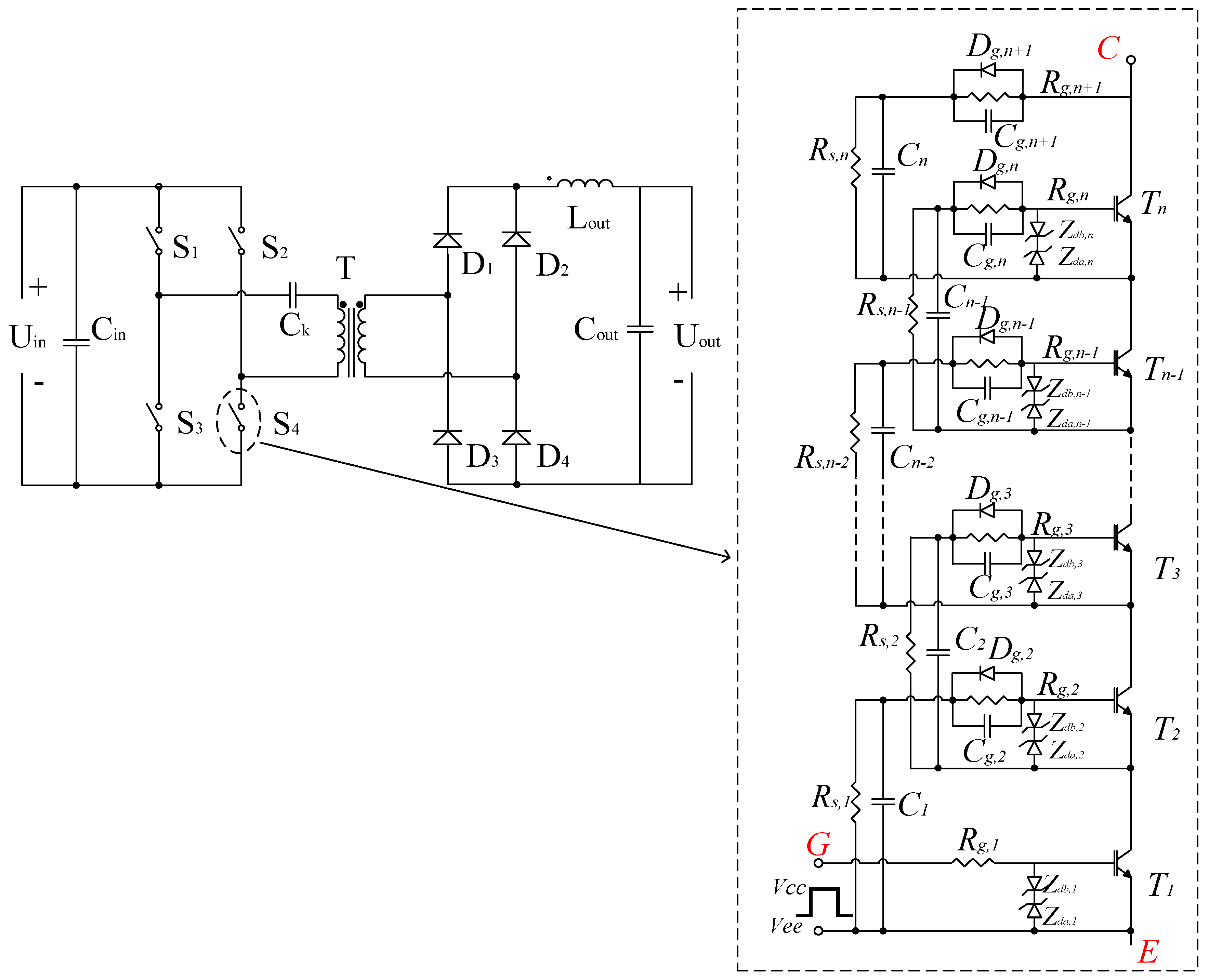
2. Schematic of the Proposed DC/DC Converter

The schematic of the proposed DC/DC converter is shown in Figure 1. The converter can adopt a mature converter topology, as the switching modules with power devices in series can withstand the input voltage level. The PSFB topology is adopted in the design, as it has smaller voltage stress and higher power output than other topologies. The primary side of the PSFB converter consists of four power switching modules, each of which only requires one independent isolated driver.
Table 1 shows the comparison among different MV DC/DC converter schemes. The proposed converter has advantages in volume, efficiency, reliability, and cost. Assuming that the input voltage of the converter is N times of the blocking voltage of the power devices, the MV converter requires at least N LV converter modules in the ISOP scheme. If the LV converter modules adopt a full-bridge topology [8], the ISOP converter requires 4N isolated driver circuits. Moreover, there are complex feedback control systems and isolated signal acquisitive circuits for input voltage and output current sharing. The MV full-bridge converter based on series-connected power devices in the traditional methods also requires 4N isolated driver circuits [17]. Comparatively, the proposed MV converter only requires four isolated driver circuits, making it compact in size, simple in structure, and low in cost. ISOP converters have high conversion efficiency due to the adoption of LV power devices, but the complex control system may reduce its reliability [6,9,10,11,12]. The proposed converter adopts mature control methods, which makes it highly reliable and has good dynamic performances.

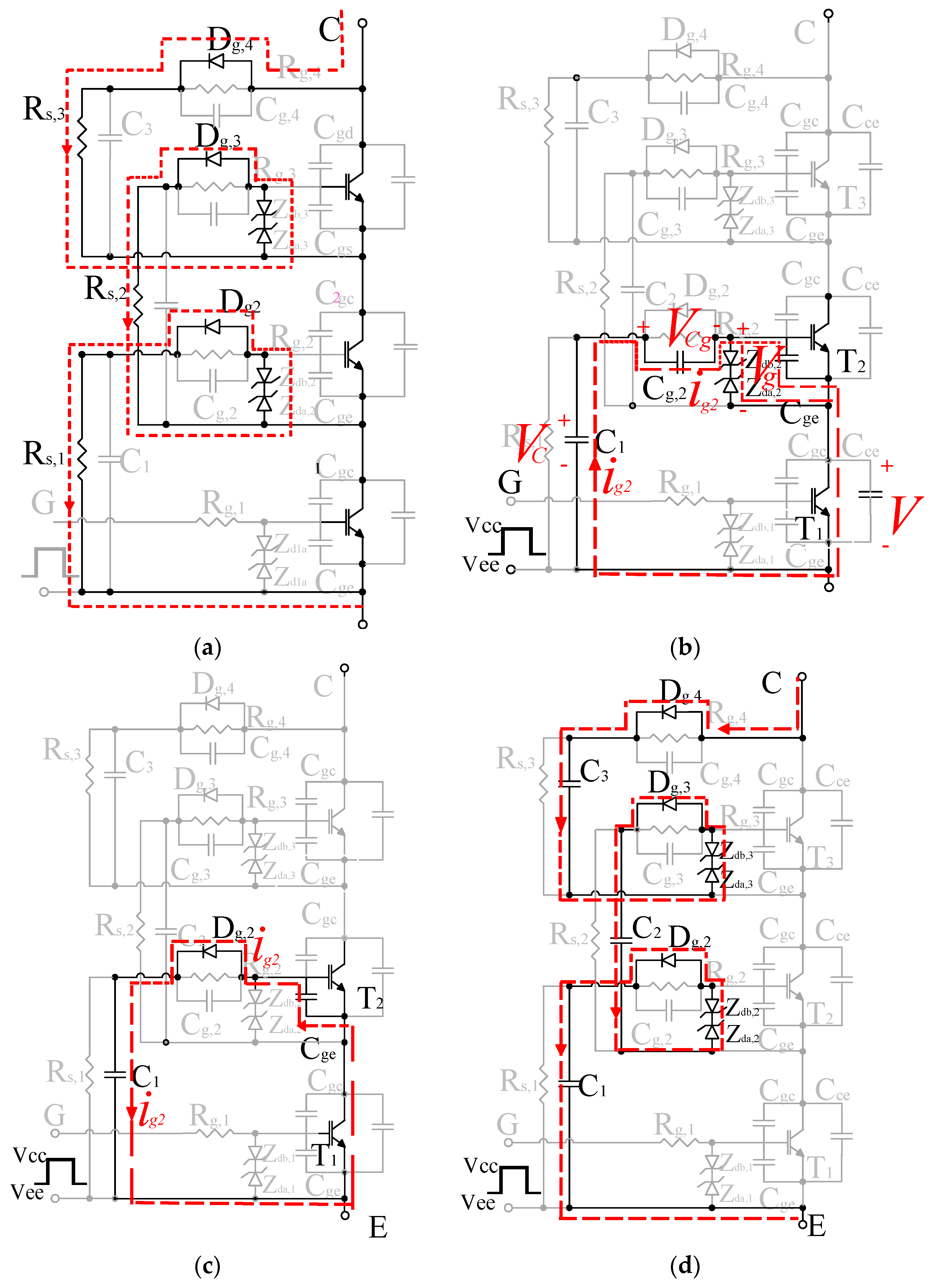
3. Series-Connected Power Switching Module

The proposed series-connected power switching module requiring only one isolated driver circuit is also shown in Figure 1. The circuit is effective for IGBTs, which are adopted in this study, and MOSFETs [23,24]. The proposed circuit is similar to, but ultimately different from, those circuits in [23,24], especially in high-frequency characteristics and scalability. Specifically, the dynamic voltage-balancing capacitors Cn, which control the upper IGBTs on-off and dynamic voltage sharing, provide the circuit with good scalability under the condition that the capacitor values are consistent, so the circuit design is more simple and controllable. Furthermore, the special arrangement of the static balancing resistors Rs,n and the gate protection zener diodes Zda,n and Zdb,n in [24] is extended for more power devices in series, not only having the function of static voltage sharing, but also providing negative gate voltages for the upper IGBTs during off state. The design of the gate diodes Dg,n, the gate resistors Rg,n, and the accelerating capacitors Cg,n in parallel makes the circuit suitable for high-frequency applications. Taking the circuit with three IGBTs in series as an example, the main current paths in different states are shown in Figure 2, and the detailed operation principle is described as follows.
Off state: When the gate voltage of the bottom IGBT remains negative, the current paths, as shown in Figure 2a, can lead to negative gate voltages for upper IGBTs. Thus, all series-connected IGBTs can keep off state. Moreover, the circuit can be simplified as a circuit in which each static balancing resistor Rg,n is connected with the corresponding IGBT in parallel. If Rg,n is far smaller than the equivalent resistance of the IGBTs, the static voltage sharing among these IGBTs can be guaranteed.
Turn-on: Once the driving signal of the driver circuit turns to a reliable positive voltage, the bottom IGBT T1 will turn on. The collector-emitter voltage Vce of T1 will decrease rapidly, so the electric potential at the collector electrode will fall quickly, which means that there is a voltage difference between the gate electrode and the source electrode of T2. Accordingly, C1 will charge the gate-emitter capacitor Cge of T2 through the current ig2 in Figure 2b, leading to an increase in the gate voltage Vg of T2. According to Kirchhoff’s Voltage Law, a circuit voltage relationship can be obtained as:
V c e + V g = V C V C g
The current ig2 can be defined as:
V c e + V g = 0 t i g 2 C n 0 t i g 2 C g , n i g 2 = V c e + V g 0 t ( 1 C n 1 C g , n )
Similarly, all upper IGBTs will turn on in sequence according to this mechanism. As described above, all charges in Cn are injected into the gate capacitor of the corresponding power device, which is different from the circuits in [23,24], and thus the proposed circuit supports more power devices in series.
The parallel connection of Rg,n and Cg,n is specially designed for high-frequency converters. According to Equation (2), if Cn is directly connected to the gate of the IGBT, i.e., 1/Cg,n is 0, the pulse currents through Zda,n and Zdb,n will be very large during each turn-on transition, leading to large energy losses on them, bringing a challenge to select small components. If only one resistor is used instead of the RC network, the turn-on speed will slow down due to the current limiting effect of the resistor. According to Equation (2), Cg,n should be larger than Cn and the pulse current increases with the increasing of Cg,n. It is necessary to balance the turn-on speed and pulse currents in the selection of Cg,n. Generally, Cg,n is double Cn according to simulation results.
On state: The driving signal of the driver circuit keeps a reliable positive voltage to ensure that T1 is in a stable on state. The Cge of upper IGBTs are charged in the turn-on transition as described above, so all IGBTs are in a stable on state. It is worth mentioning that the Cge of upper IGBTs will discharge during on state, which means Vg of upper IGBTs will decrease slowly. However, it does not matter in high-frequent converter applications as the on-time is short.
Turn-off: Once the driving signal of the driver circuit reaches a reliable negative voltage, T1 will turn off. The electric potential at the collector electrode of T1 will rise rapidly, so there will be a negative pulse voltage between the gate and emitter electrode of T2, forcing T2 to turn off. All IGBTs will turn off in sequence by this mechanism. The main current paths in this period are shown in Figure 2c. When all IGBTs are in off state, there is still a charging current for Cn as shown in Figure 2d. With the charging of Cn, when the voltage across the switching module rises to the bus voltage Vbus, the turn-off transition ends. Since each level has the same structure, all IGBTs turn off from the bottom to the top in sequence with the same voltage slope. Therefore, the voltage distribution among all IGBTs is controllable. As the lower IGBTs turn off earlier, the Vce of them will be larger. The voltage differences between adjacent IGBTs are equal and related to Cn.
The switching loss is a key factor to be considered in high-frequency applications. During the turn off transition, the charging process of Cn brings extra energy loss Eoff, which can be defined as follows:
E off = 1 2 N C n V ds 2 = C n V b u s 2 2 N

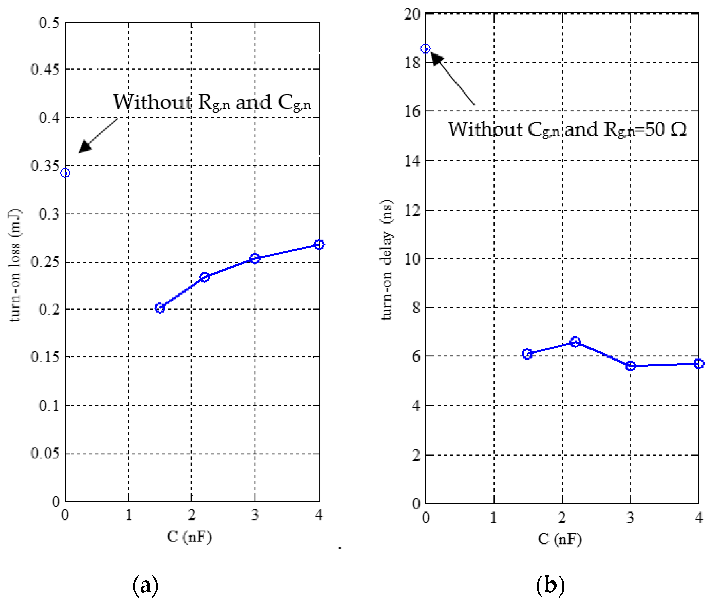
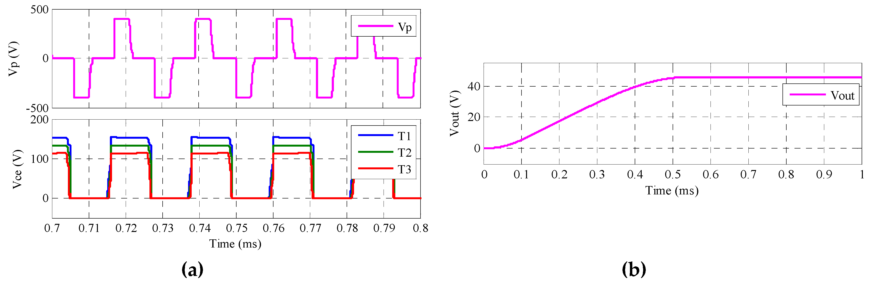
4. Simulation Verification

To verify the feasibility of the proposed series-connected power switching module and the effect of the accelerating capacitors on the circuit, double pulse tests are simulated in LTspice. The waveforms, as shown in Figure 3, validate the proposed circuit drivers the series-connected power devices efficiently. Moreover, the voltage sharing among the three power devices is realized during both static and dynamic transitions. As shown in Figure 4a, the turn-on loss on gate protection zener diodes Zda,2 and Zdb,2 is maximum when both Rg,n and Cg,n are 0, and increases with the increasing of the accelerating capacitors Cg,n, which agrees with Equation (2). Moreover, it can be seen from Figure 4b that the increasing of the accelerating capacitors can significantly reduce the turn-on delay, but the value of the accelerating capacitors has little effect on it.
To verify that the proposed switching module can be applied to the PSFB topology, a simulation of a converter using three series-connected IGBTs in each switching module is performed in LTspice. The critical parameters of the simulation are shown in Table 2.
The waveform of the transformer primary voltage in Figure 5a verifies that the primary side of the proposed converter can convert DC into alternating current (AC) power. The voltage distribution in the switching module agrees with the theoretical analysis. The maximum voltage difference among the IGBTs is 41.8 V. The output voltage in Figure 5b stabilized to about 48 V after a short ascent, proving the feasibility of the converter design.

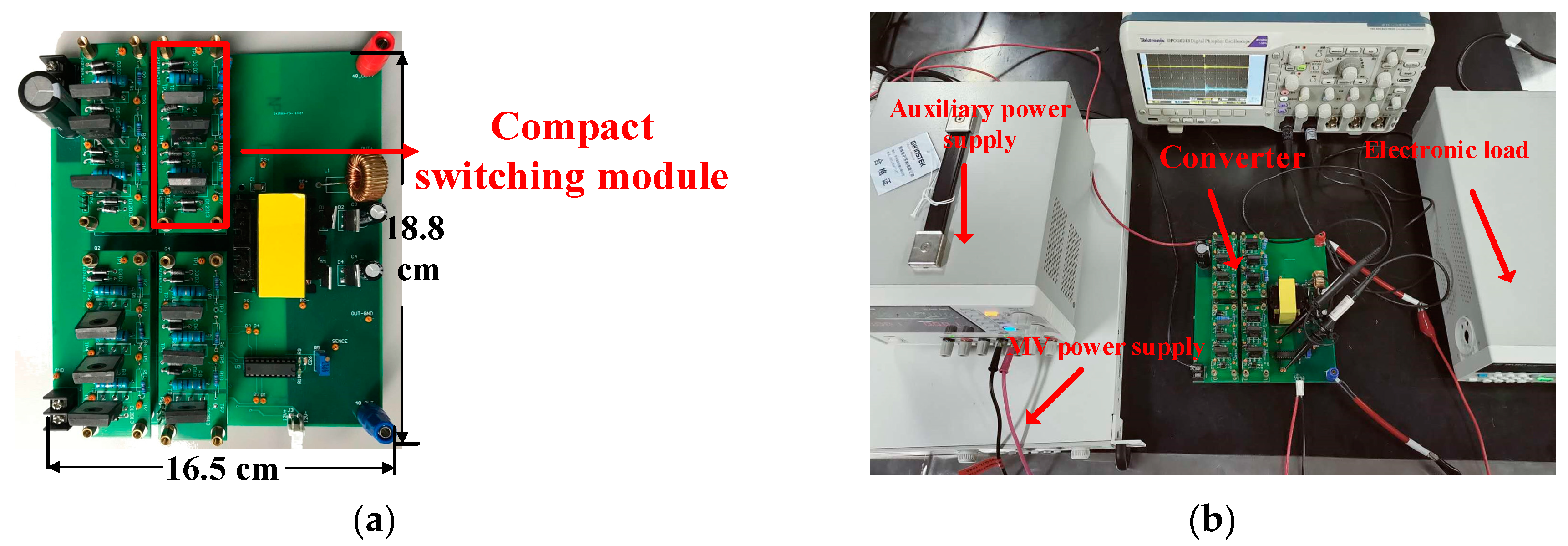
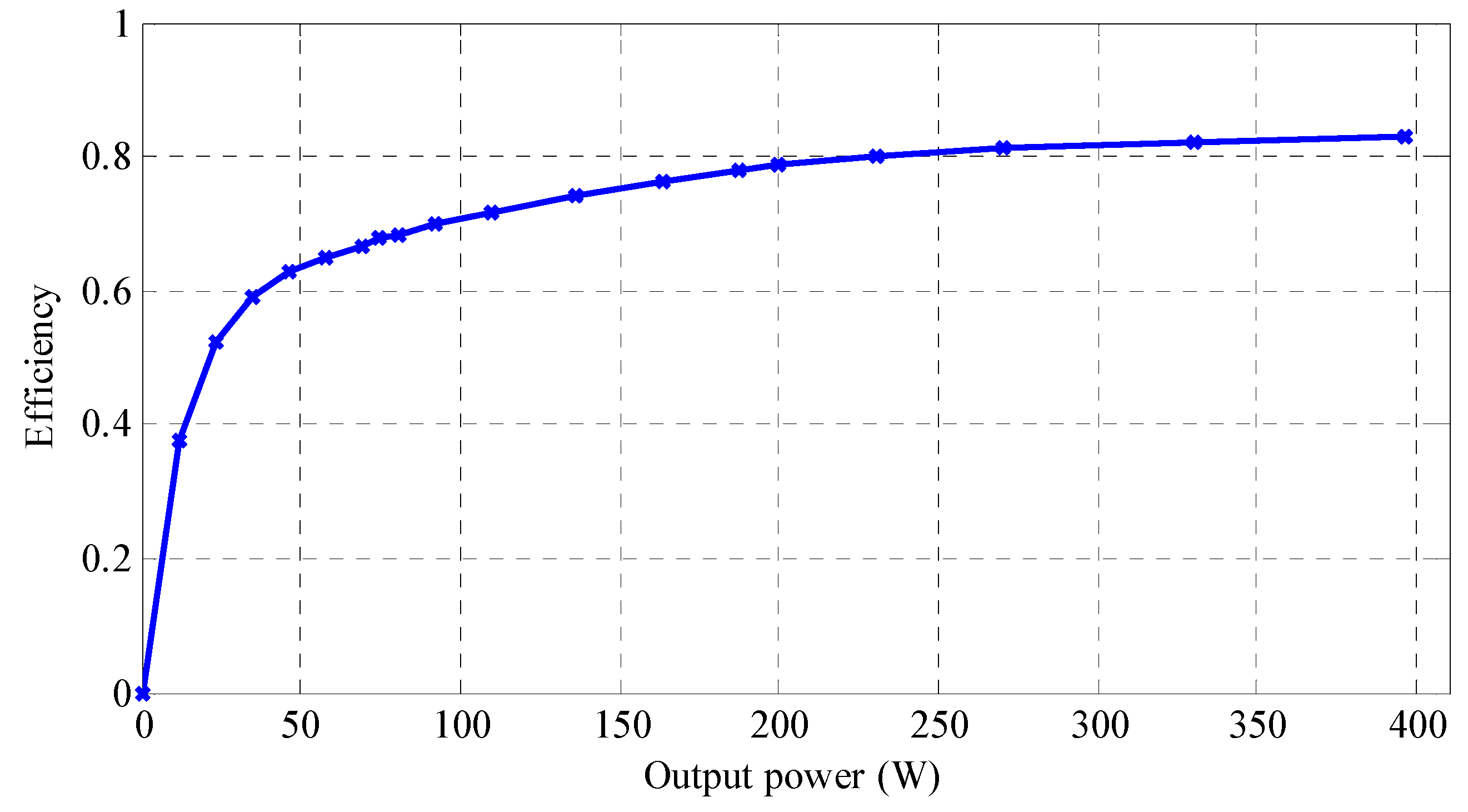
5. Experiment Verification

A prototype with three series-connected IGBTs in each switching module, shown in Figure 6a, was developed to verify the converter design. The critical parameters of the prototype are also given in Table 2. The control circuit is based on phase shift resonant controller integrated circuits. The photograph of the test setup is shown in Figure 6b.
As shown in Figure 7a,b, the proposed switching module can turn on and off continuously. Figure 7c,d verify that the full-bridge topology consisting of 4 switching modules converts DC into AC power. The phase difference between the leading and lagging legs changes as shown in Figure 7, so that the output voltage is stable under different loads. The maximum voltage difference of the power devices within the switching module is about 40 V, which is consistent with the simulation result. It is almost unchanged under different loads, as shown in Figure 8.
The efficiency curve of this converter is shown in Figure 9. It can be seen that the efficiency increases with the load, consistent with general DC/DC converters. There is no maximum conversion efficiency point in Figure 9, so further increase of the load may continuously improve the conversion efficiency. The efficiency at 400 W load is about 83.1%, greater than the efficiency (63.8%) of the converter based on traditional methods for series-connected power devices in [14], but less than the efficiency (95%) of ISOP converters in [10]. The measured switching loss of each module is about 0.15 mJ, larger than the theoretical value according to Equation (3). The reason for this is that the switching loss of the IGBTs with high blocking voltages is large, so choosing a more suitable power device can improve the efficiency. As the proposed converter can adopt a mature control scheme and topology, realizing soft switching is also an effective way to further improve the conversion efficiency.

6. Conclusions

This letter proposes a compact MV DC/DC converter using series-connected power devices. The converter applies the mature PSFB topology and control method, so it has high stability and dynamic performances compared with ISOP converters. The power switching module, composed of several passive components and power devices in series, and with only one external isolated driver circuit, is the key of this converter. Based on the modules, the proposed converter requires only four isolated driver circuits, making it compact, simple in structure, and cost-effective. The operation principle of the switching module is analyzed and the feasibility of the design is verified by simulations and experiments. The switching module can also be used in other high-frequency and high-voltage applications. The characteristics of this converter in soft switching mode are worthy to be studied to achieve higher efficiencies.

Author Contributions

Conceptualization, F.L.; methodology, F.L.; validation, F.L.; formal analysis, S.Z.; investigation, S.Z. and F.L.; resources, F.L.; data curation, S.Z.; writing—original draft preparation, S.Z.; writing—review and editing, F.L.; visualization, S.Z.; supervision, F.L.; project administration, F.L.; funding acquisition, F.L. All authors have read and agreed to the published version of the manuscript.

Funding

This work was supported in part by the National Natural Science Foundation of China under Grant 61936014, the Shanghai Science and Technology Innovation Initiative under Grant 16DZ1205000, and the State Key Lab of Marine Geology under Grant MG20204.

Conflicts of Interest

The authors declare no conflict of interest.

References

  1. Inoue, S.; Akagi, H. A Bidirectional Isolated DC–DC Converter as a Core Circuit of the Next-Generation Medium-Voltage Power Conversion System. IEEE Trans. Power Electron. 2007, 22, 535–542. [Google Scholar] [CrossRef]
  2. Howe, B.M.; Kirkham, H.; Vorperian, V. Power system considerations for undersea observatories. IEEE J. Ocean. Eng. 2002, 27, 267–274. [Google Scholar] [CrossRef]
  3. Al-Haiki, Z.E.; Shaikh-Nasser, A.N. Power Transmission to Distant Offshore Facilities. IEEE Trans. Ind. Appl. 2011, 47, 1180–1183. [Google Scholar] [CrossRef]
  4. Siri, K.; Willhoff, M.; Conner, K. Uniform Voltage Distribution Control for Series Connected DC–DC Converters. IEEE Trans. Power Electron. 2007, 22, 1269–1279. [Google Scholar] [CrossRef]
  5. Vorperian, V. Synthesis of Medium Voltage dc-to-dc Converters From Low-Voltage, High-Frequency PWM Switching Converters. IEEE Trans. Power Electron. 2007, 22, 1619–1635. [Google Scholar] [CrossRef]
  6. Giri, R.; Choudhary, V.; Ayyanar, R.; Mohan, N. Common-duty-ratio control of input-series connected modular DC-DC converters with active input voltage and load-current sharing. IEEE Trans. Ind. Appl. 2006, 42, 1101–1111. [Google Scholar] [CrossRef]
  7. Cha, H.; Ding, R.; Tang, Q.; Peng, F.Z. Design and Development of High-Power DC-DC Converter for Metro Vehicle System. IEEE Trans. Ind. Appl. 2008, 44, 1795–1804. [Google Scholar] [CrossRef]
  8. Fan, H.; Li, H. High-Frequency Transformer Isolated Bidirectional DC–DC Converter Modules With High Efficiency Over Wide Load Range for 20 kVA Solid-State Transformer. IEEE Trans. Power Electron. 2011, 26, 3599–3608. [Google Scholar] [CrossRef]
  9. Ayyanar, R.; Giri, R.; Mohan, N. Active input-voltage and load-current sharing in input-series and output-parallel connected modular DC-DC converters using dynamic input-voltage reference scheme. IEEE Trans. Power Electron. 2004, 19, 1462–1473. [Google Scholar] [CrossRef]
  10. Jung-Won, K.; Jung-Sik, Y.; Cho, B.H. Modeling, control, and design of input-series-output-parallel-connected converter for high-speed-train power system. IEEE Trans. Ind. Electron. 2001, 48, 536–544. [Google Scholar] [CrossRef] [Green Version]
  11. Kimball, J.W.; Mossoba, J.T.; Krein, P.T. A Stabilizing, High-Performance Controller for Input Series-Output Parallel Converters. IEEE Trans. Power Electron. 2008, 23, 1416–1427. [Google Scholar] [CrossRef]
  12. Ruan, X.; Chen, W.; Cheng, L.; Tse, C.K.; Yan, H.; Zhang, T. Control Strategy for Input-Series-output-Parallel Converters. IEEE Trans. Ind. Electron. 2009, 56, 1174–1185. [Google Scholar] [CrossRef]
  13. Mohammadpour, A.; Parsa, L.; Todorovic, M.H.; Lai, R.; Datta, R.; Garces, L. Series-Input Parallel-Output Modular-Phase DC–DC Converter with Soft-Switching and High-Frequency Isolation. IEEE Trans. Power Electron. 2016, 31, 111–119. [Google Scholar] [CrossRef]
  14. Yaqiang, H.; Wenjie, C.; Xiliang, C.; Xin, M.; Yilin, S.; Xu, Y.; Xiang, L. A 4000V input auxiliary power supply with series connected SiC MOSFETs for MMC-based HVDC system. In Proceedings of the 2016 IEEE 8th International Power Electronics and Motion Control Conference (IPEMC-ECCE Asia), Hefei, China, 22–26 May 2016; pp. 279–284. [Google Scholar]
  15. Ji, S.; Zheng, S.; Wang, F.; Tolbert, L.M. Temperature-Dependent Characterization, Modeling, and Switching Speed-Limitation Analysis of Third-Generation 10-kV SiC MOSFET. IEEE Trans. Power Electron. 2018, 33, 4317–4327. [Google Scholar] [CrossRef]
  16. Lemmon, A.N.; Graves, R.C.; Kini, R.L.; Hontz, M.R.; Khanna, R. Characterization and Modeling of 10-kV Silicon Carbide Modules for Naval Applications. IEEE J. Emerg. Sel. Top. Power Electron. 2017, 5, 309–322. [Google Scholar] [CrossRef]
  17. Abbate, C.; Busatto, G.; Iannuzzo, F. High-Voltage, High-Performance Switch Using Series-Connected IGBTs. IEEE Trans. Power Electron. 2010, 25, 2450–2459. [Google Scholar] [CrossRef]
  18. Baraia, I.; Barrena, J.A.; Abad, G.; Segade, J.M.C.; Iraola, U. An Experimentally Verified Active Gate Control Method for the Series Connection of IGBT/Diodes. IEEE Trans. Power Electron. 2012, 27, 1025–1038. [Google Scholar] [CrossRef]
  19. Ju Won, B.; Dong-Wook, Y.; Heung-Geun, K. High-voltage switch using series-connected IGBTs with simple auxiliary circuit. IEEE Trans. Ind. Appl. 2001, 37, 1832–1839. [Google Scholar] [CrossRef]
  20. Finney, S.J.; Williams, B.W.; Green, T.C. RCD snubber revisited. IEEE Trans. Ind. Appl. 1996, 32, 155–160. [Google Scholar] [CrossRef] [Green Version]
  21. Zhang, L.; Sen, S.; Huang, A.Q. 7.2-kV/60-A Austin SuperMOS: An Intelligent Medium-Voltage SiC Power Switch. IEEE J. Emerg. Sel. Top. Power Electron. 2020, 8, 6–15. [Google Scholar] [CrossRef]
  22. Lim, T.C.; Williams, B.W.; Finney, S.J.; Palmer, P.R. Series-Connected IGBTs Using Active Voltage Control Technique. IEEE Trans. Power Electron. 2013, 28, 4083–4103. [Google Scholar] [CrossRef]
  23. Teerakawanich, N.; Johnson, C.M. Design Optimization of Quasi-Active Gate Control for Series-Connected Power Devices. IEEE Trans. Power Electron. 2014, 29, 2705–2714. [Google Scholar] [CrossRef]
  24. Ren, Y.; Yang, X.; Zhang, F.; Wang, K.; Chen, W.; Wang, L.; Pei, Y. A Compact Gate Control and Voltage-Balancing Circuit for Series-Connected SiC MOSFETs and Its Application in a DC Breaker. IEEE Trans. Ind. Electron. 2017, 64, 8299–8309. [Google Scholar] [CrossRef]
Figure 1. Schematic of the proposed DC/DC converter.
Electronics 09 01024 g001
Figure 2. Main current paths in the proposed circuit in different states: (a) Off state; (b) turn-on transition; (c) turn-off transition; (d) turn-off transition.
Electronics 09 01024 g002
Figure 3. Simulation waveforms when the DC bus voltage is 3000 V, Cn = 1 nC and Cn,g = 2.2 nC: (a) Waveforms of a double-pulse test; (b) close-up view of waveforms during turn-on transition; (c) close-up view of waveforms during turn-off transition.
Electronics 09 01024 g003
Figure 4. Simulation results with different accelerating capacitors when the DC bus voltage is 3000 V and Cn=1 nC: (a) The turn-on loss on gate protection zener diodes Zda,2 and Zdb,2; (b) the turn-on delays.
Electronics 09 01024 g004
Figure 5. Simulation waveforms under 200 W load: (a) Primary voltage of the transformer and voltage distribution in S1; (b) output voltage.
Electronics 09 01024 g005
Figure 6. (a) Photograph of the DC/DC converter prototype; (b) the photograph of the experimental setup.
Electronics 09 01024 g006
Figure 7. Experiment waveforms: (a) The voltages across S1 and S2 (no-load); (b) the voltages across S1 and S2 (200 W load); (c) the primary voltage of the transformer (no-load); (d) the primary voltage of the transformer (200 W load).
Electronics 09 01024 g007
Figure 8. The voltage distribution in S1 under different loads: (a) Under no-load; (b) under 200 W load.
Electronics 09 01024 g008
Figure 9. Efficiencies under different loads.
Electronics 09 01024 g009
Table 1. Comparison among different MV DC/DC converter schemes.
MV DC/DC convertersVolumeEfficiencyReliabilityCost
ISOP convertersMediumHighMediumHigh
Traditional converters with series-connected power devicesLargeLowLowHigh
The proposed converterSmallMediumHighLow
Table 2. Critical parameters in the simulation.
ComponentValueDescription
Vin400 VInput voltage
Vout48 VOutput voltage
f50 kHzSwitching frequency
TnIXBH42N1701700 V IGBT
Rg,n50 ΩGate resistors
Rs,n510 KΩStatic voltage-balancing resistors
Zda,n and Zdb,n1N5352B15 V zener diode
Dg,nSF16001600 V fast recovery diode
Cn2.2 nFDynamic voltage-balancing capacitors
Cg,n4.7 nFGate accelerating capacitors

