1. Introduction
The infrared (IR) detector is a radiant energy transducer, which is mainly used to convert the IR radiation energy into electrical energy, thermal energy, and other forms of energy that are convenient for measurement or observation. Generally, there are two kinds of IR detectors: Thermal detectors and photonic detectors. Thermal detectors rely on temperature-induced changes in the physical properties of the material when exposed to IR radiation, which can perform at room temperature and cryogenic cooling is not needed [
1,
2]. However, thermal detectors have lower resolution and slower response time compared with photonic detectors [
3,
4]. In recent years, uncooled IR detectors have received tremendous attention with the development of micro-electromechanical systems (MEMS), due to their advantages of low cost, miniaturization, and ultra-low power. Many applications have been developed, such as thermography, human detection, night vision, etc. There are several types of thermal detectors, including bolometers, thermopiles, pyroelectric detectors, and resonant detectors [
5,
6,
7,
8,
9].
Advanced thermal detectors based on aluminum nitride (AlN) Lamb-wave resonators (LWRs) are drawing significant attention due to their small size, complementary metal-oxide-semiconductor (CMOS) compatible process, high performance, low cost, and low power [
9,
10,
11]. The MEMS resonant detectors could achieve high detection sensitivity, and ultra-low noise performance. The resonant detectors are passive IR detectors, which can sense IR radiation without the need for additional optical equipment. When IR radiation is absorbed by the resonant detectors, their temperature will rise, which may cause a measurable frequency shift of the Lame-wave resonant mode. Frequency shift is a physical quantity that can be monitored with the highest precision by simply measuring the zero crossings digitally. In addition, AlN LWRs can obtain high frequency as well as high quality factor (
Q-factor), which can further enhance their thermal sensitivities. The detectors based on AlN LWRs show great potential applications. However, how to achieve high IR radiation absorption is the key for their implementation.
Metasurfaces, engineered by plasmonic resonances, have attracted considerable interest due to their outstanding optical properties, which have been used in extensive applications, such as transmission, absorbers, etc. [
12,
13,
14]. The plasmon metasurface can be maintained by a subwavelength-size nanoarray to achieve super absorption [
15]. Plasmon metasurface absorbers are mainly classified into three types of structures: Plasmon crystal [
16], metal-insulator-metal (MIM) [
17], and mushroom structures [
18]. In these three types, MIM absorbers have the simplest structures as well as fabrication processes, and also can be easily adjusted by their sizes or structures to achieve ultrahigh as well as selective absorption. Generally, the plasmon absorber with a metal-insulator-metal (MIM) structure has a subwavelength-size array and a bottom metal layer on the upper and lower surfaces of the insulation film, respectively [
15,
17,
19,
20]. In the last few years, an uncooled MEMS resonant IR detector, composed of a plasmon metasurface absorber with a square structure, has been demonstrated to achieve ultra-high IR absorption and controllable absorption spectra [
10]. Compared with other types of thermal detectors, the detector not only shows enhanced sensitivity due to the high accuracy in high-frequency readout, but do not need direct-current (DC) driving. However, the subwavelength-size array integrated on the top of the detector, not metal plane, has a direct influence on its electric-field excitation, which could deteriorate its electrical performances, including
Q-factor, electromechanical coupling coefficient (
), and signal-to-background ratio (SBR). In addition, it is not easy to adjust the subwavelength-size array to achieve dual-band absorption which is particularly important with regard to analytical sensing applications, such as gas and material sensing [
21].
Moreover, it is important to consider thermal behaviors of the resonant detector, which have strong influences on the detector’s sensitivity and response time. Thermal behaviors of the detector include temperature coefficient of frequency (TCF), thermal time τ, and thermal resistance Rth. TCF is defined as the sensitivity of the resonance frequency to temperature. For example, as two detectors rise to the same degree of temperature, a detector with the larger TCF can yield a larger frequency shift. The thermal time directly affects the response time of the device. For the similar amount of IR radiation, the higher thermal resistance of the device will induce a higher temperature rise, which contributes to a higher sensitivity.
This work presents an AlN LWR integrated with a subwavelength aperture array for IR detection. The integrated absorber can not only achieve dual-band IR detection, but also its plane-like structure can maintain the electrical performance of the detector. The resonant performance, IR absorption, thermal behaviors were systematically studied by theoretical analysis, as well as using the finite element method (FEM) and finite difference time domain (FDTD) simulations.
2. Structure Design and Discussion
An AlN piezoelectric resonant IR detector was designed as shown in
Figure 1. The detector is based on an LWR with the suspended free-edge reflectors. It is composed of a 500 nm-thick AlN film sandwiched between two metal layers. The top Au layer with the thickness of 50 nm is patterned to form an array of cross-shaped apertures. The appropriate dimension of the apertures can contribute to achieving ultrahigh dual-band absorption in the IR range. The bottom Mo layer with the thickness of 200 nm is patterned to form interdigital transducers (IDTs) to actuate and to sense Lamb-wave modes in the AlN film. The Lame-wave resonant frequency mainly depends on the period
P of IDTs [
22]. The suspended free edges are not only formed as solid-air interfaces to reflect Lamb waves, but they can also increase the thermal resistance
Rth. The main dimensional parameters of the resonator are marked in
Figure 1b. The wavelength (
λ) of Lamb wave is twice of the period
P of IDTs. The thickness, length, and width of the AlN film are labeled as
tAlN,
L, and
W, respectively. In addition,
W0 represents the width of the IDT finger electrodes.
As the IR radiation is absorbed by the presented detector, it will induce a temperature rise of the detector, which in turn causes a frequency shift due to the detector’s TCF. The top Au layer is patterned to form a plasmon metasurface, with a goal to improve the IR absorption, which can significantly promote the overall detector responsivity. With the increasing of the responsivity, the important performance indicators, including the noise equivalent power and detectivity, are simultaneously enhanced, which contributes to an enhanced capability of detecting weak signals and thereby a higher detection accuracy.
2.1. Resonant Characteristics
The resonant performances of the AlN resonant IR detector, including resonant frequency
fs,
Q-factor,
, and SBR, have a direct impact on IR detection performances, which may be significantly deteriorated by the top plasmon array. Due to the plasmon array on the surface of the AlN film, only a single-IDT electrode structure can be used to excite the detector operating at a Lame-wave mode.
Figure 2 shows the sectional illustrations of the AlN LWRs with open and floating electrode configurations. The electrode configurations can affect the static capacitances
C0 and the electric-field excitation between radio-frequency (RF) signal and ground ports [
23]. The
C0 of the open-electrode configuration can be simplified to be equal to the lateral capacitance
Cl. For the floating electrode, the
C0 is dependent on the lateral capacitance
Cl and the vertical capacitance
Cv, which can be assumed to be the sum of
Cl and
Cv/2. The
Cl and
Cv control the lateral-field excitation and thickness-field excitation, respectively. Therefore, the floating-electrode configuration could be a contributing factor in achieving a better resonant performance.
In order to optimize the detector’s electrical performance, a subwavelength aperture array was designed on the surface of the AlN film. The structures with the floating electrode, particle array, and open electrode are presented in
Figure 3. The resonant performances of the four structures were numerically analyzed by using the Comsol Multiphysics software. The material properties of Au, AlN, and Mo used in the simulation studies were referred to in [
24,
25]. The device length, IDT pitch, number of IDT fingers, and IDT width were set to be 60, 6, 7, and 3.6 μm, respectively. As shown in
Figure 3, the simulated resonant mode of the device with the plasmon apertures has a small difference with the floating-electrode device, which is due to its large metal-coating ratio. However, the simulated results show that the devices with the particle array and open electrode have similar resonant modes, which distort from the Lame-wave mode due to a weak electric-field excitation. Furthermore, admittance amplitude spectra of four device structures were calculated, as shown in
Figure 4. The SBRs of the devices with the particle array and open electrode are approximately 0.7 and 0.8 dB due to low
, respectively, which result in difficult detection of resonant signals. The SBR is an important indicator of resonance intensity, which can be defined as the difference between the maximum admittance amplitude and the background noise around the resonance peak. The electrical performance of the device with the aperture array is slightly worse than that of the floating-electrode device, but obviously superior to that of the other two structures. In summary, the designed AlN resonant IR detector with the plasmon aperture array can maintain electrical performances well.
2.2. IR Absorption Properties
In this work, an Au subwavelength aperture array was designed on the top of the AlN film in order to achieve ultrahigh and dual-band IR absorption, as shown in
Figure 5. The lattice period
a of this rectangular hole array was 3 μm, and the length
la and width
lb of the rectangle were 2.4 and 0.1 μm, respectively. The thickness of the dielectric layer
tAlN was set as 500 nm. The absorption properties of the structures could be calculated by using the Lumerical FDTD Solutions software. The polarization orientation of the incident radiation was parallel to the Y-axis and defined as polarization angle 0°. The incident angle was perpendicular to the absorber to study the basic detection performance. The real and imaginary refractive index of Au, AlN, and Mo were derived from [
26,
27,
28]. The absorbance was calculated using the equation
A = 1 −
R −
T, where
A,
R, and
T are the absorption, reflectance, and transmittance of the structure, respectively. As shown in
Figure 5c, the simulated results show that the absorption spectrum of this structure has two absorption peaks, which are located at 5.5 and 7.8 μm. The maximum absorptions of the two peaks are 97.0% and 99.5%, and full widths at half maximums (FWHMs) are 0.14 and 0.4 μm, respectively. The absorptions of non-resonant bands are near zero. The results demonstrate that the proposed plasmon array is a favourable double-band absorption structure.
In order to further analyze the mechanism of the dual-band absorption, the electric and magnetic fields of the two resonance peaks were explored. In
Figure 6, it obviously shows that the rectangular aperture array structure has two resonance modes. As the wavelength is 5.5 μm, the magnetic resonance is mainly concentrated in the dielectric layer below the rectangular hole, which belongs to a fundamental-mode resonance or a inductor-capacitor (LC) resonance. When the wavelength is 7.8 μm, the magnetic resonance is mainly localized at the dielectric layer between the lattices. This resonance mode is mainly due to the interaction between the lattices, which is a high-order resonance. For the LC resonance mode of a rectangular hole, the resonance frequency
ω can be expressed as [
29]:
where
L1,
L2, and
C represent the inductance and capacitance, respectively. For the rectangular aperture array,
L1 is the same as
L2. The value of
C is proportional to
lb, and the value of
L1 is proportional to
la. Based on the fundamental-mode resonance and high-order resonance of the lattice structure, the dual-band absorption is obtained.
Furthermore, with the fixed lattice period
a = 3 μm and width
lb = 0.1 μm, the effect of the length
la of the rectangular aperture array on the absorption spectrum was studied, as shown in
Figure 7a. As
la increases from 1.6 to 2.4 μm, the LC resonance absorption peak redshifts from 6.6 to 7.8 μm. According to the LC resonance frequency formula (1), the LC resonance frequency
ω decreases with the increase of
la, which is consistent well with the simulated results. Due to the fixed lattice period
a, the gap between the lattices decreases with the increase of
la, and then the capacitance between the lattices increases, leading to the high-order resonance wavelength redshifting. The calculated results agree with the corresponding theoretical analysis, and the dual-band absorption peak can be adjusted by changing
la. Moreover, the effect of the polarization angle on the absorption spectrum of the rectangular-aperture absorber was simulated, as shown in
Figure 7b. As the polarization angle increases from 0 to 90°, the absorption is severely attenuated. In particular, when the polarization angle is 90°, the absorber could not induce a plasmon resonance. The results show that the absorber is sensitive to the polarization, due to the fact that the rectangular-aperture array is not a four-fold rotational symmetry.
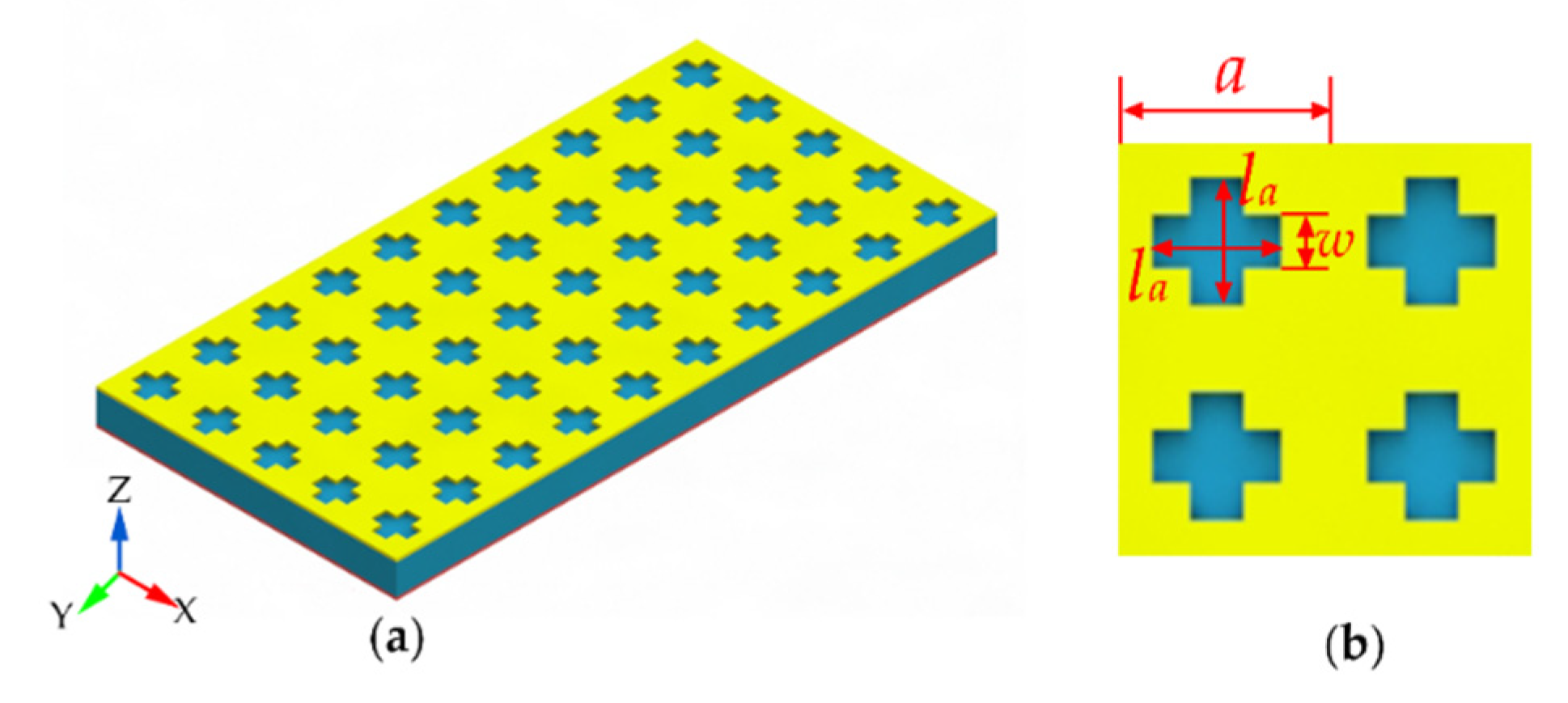
In order to achieve polarization-independent absorption, a cross-shaped aperture absorber was designed in
Figure 8, showing a four-fold rotational symmetry structure [
30]. The geometric parameters of this absorber were set as
a = 3 μm,
la = 2.4 μm,
lb = 2.4 μm,
w = 50 nm.
Figure 9a illustrates the absorption spectra of the cross-shape aperture absorber for different polarization angles. It is clear that the absorption spectra are unchanged with the polarization angles. There also exists two resonance absorption peaks at 5.4 and 7.8 μm, and the maximum absorptions of the two peaks are 85.6% and 97.1%, respectively. Similar to the above rectangle aperture absorber, the LC resonance frequency can be adjusted by changing
la. As shown in
Figure 9b, the absorption peak redshifts from 7.2 to 8.1 μm with
la increasing from 2 to 2.5 μm.
The influence of the incident angle on the absorption spectrum of the cross-shaped aperture absorber was simulated, as shown in
Figure 10. With the incident angle ranging from 0 to 75°, the locations and maximum absorptions have minor changes for the fundamental and high-order resonances. However, the absorptions of non-resonant bands are increased due to a Fabry-Perot resonance between the cross-shaped aperture and its air gap. As IR radiation is incident at an angle, a part of IR radiation is confined in the Fabry-Perot cavity. Fortunately, the resonance intensity of the Fabry-Perot resonance is much weaker than that of the fundamental and high-order resonances.
2.3. Thermal Properties
Temperature coefficient of frequency (
TCF) is one of the thermal properties of the resonant IR detector, which indicates the relative shift in resonance frequency over temperature. The
TCF mainly depends on the temperature coefficient of elasticity (
TCE) as well as the thermal expansion coefficient of AlN, which can be expressed as follows:
where
fs(
T0) is the resonant frequency at temperature
T0;
fs(
T1) is the resonant frequency at temperature
T1;
α is the frequency shift caused by the thermal expansion coefficient in the Lamb-wave propagation direction (X-axis), which is approximately 4.15 ppm/K [
31]. The frequency shift, caused by the
TCE of AlN, was calculated by using the COMSOL Multiphysics software, as shown in
Figure 11. The
TCF ≈ (−15.79–4.15) ppm/K = −19.94 ppm/K shows a linear frequency-temperature characteristic, which could contribute to an accurate IR detection.
The thermal time constant
τ is an important parameter, which defines the response speed of the detector. The
τ is the required time of the detector rising to 63.2% of the thermal equilibrium temperature after receiving IR radiation. When a thermal equilibrium is reached, the dissipated and absorbed heat power of the detector is balanced. The schematic diagram of heat transfer of the detector is shown in
Figure 12a.
Pin is the input IR power, and
T1,
T0 are the temperature of the device and Si substrate, respectively. There exists three different heat transfers from the detector to the Si substrate, including conduction, convection, and radiation. The convection is the heat transfer between objects with different temperatures by the air movement, which can be regarded as a natural convection between all device surfaces and the surrounding air in the simulation model. The radiation is an electromagnetic radiation emitted from the device to the Si substrate and surrounding air, which has little influence on the detector’s thermal properties due to the detector operating at room temperature. In the COMSOL Multiphysics software, the natural convection and radiation can be set in the module of solid heat transfer. Since the detector has a much smaller size compared with the substrate and the surrounding air, it is assumed in this work that the absorbed IR power would not affect the temperature of the substrate and the air, and the ambient temperature
T0 was fixed at 293.15 K.
In this work, the dimensions of two anchors were focused to improve the thermal performance of the detector, and its schematic illustration is shown in
Figure 12b. In COMSOL Multiphysics software, the input power (
Pin), and the anchor dimension were set as 1 μW and 5 μm × 12 μm, respectively. The increased detector temperature Δ
T is defined as
T1–
T0, and the higher Δ
T means the larger frequency shift. At the status of thermal equilibrium, the temperature distribution of the detector is relatively uniform, and the heat conduction mainly occurs between the anchors and the Si substrate, as shown in
Figure 13a. In
Figure 13b, the blue and red lines represent the temperature profiles on the anchors and the resonator, respectively, and the temperature variation among the whole device is found to be only 5.14 mK. Additionally, the thermal performances of the detector with different anchor dimensions, including
τ, Δ
T, and thermal resistance (
Rth), were calculated as shown in
Table 1. The results demonstrate that the anchors play an important role in the thermal performances. The detector with narrower and longer anchors could contribute to achieving higher Δ
T and
Rth, but its response speed is lower. Therefore, it should be mentioned that the responsivity and response speed should be considered in order to optimize the anchor dimension.
In general, the resonant IR detector requires vacuum encapsulation to maintain long-term stability as well as a high
Q-factor. The influence of vacuum encapsulation on the detector’s thermal response was calculated as shown in
Figure 14. The
τ and Δ
T of the vacuum encapsulated detector are 118 μs and 22.8 mK, and these of the non-vacuum encapsulated detector are 111 μs and 21.7 mK, respectively. Compared to the non-vacuum encapsulated detector, the vacuum encapsulated detector has slightly higher Δ
T and longer
τ due to the inexistence of the natural convection between the detector and vacuum environment. The heat conduction plays a major role in the heat transfer through Mo/AlN anchors, especially Mo has a higher thermal conductivity. Therefore, the vacuum encapsulation of the detector has little effect on its thermal response.
3. Conclusions
In this work, an AlN piezoelectric resonant IR detector with a subwavelength aperture array was designed. The subwavelength aperture array can maintain the resonant performance of the detector due to its large metal-coating ratio. It can also achieve ultrahigh dual-band IR absorption due to the fundamental-mode resonance and high-order resonance of the lattice structure. The IR absorption properties of the detector were systematically studied by using the Lumerical FDTD Solutions software. The geometric parameters of the aperture array were optimized to achieve the dual-band absorptions of up to 97%, with polarization-independent absorption, which have excellent IR absorbance properties.
In addition, thermal properties of the detector, including temperature coefficient of frequency TCF, thermal time constant τ, and increased temperature ΔT, were explored by using the COMSOL Multiphysics software. The calculated results show that the TCF is approximately −19.94 ppm/K. The τ and ΔT mainly depend on the conduction between the detector and Si substrate, which can be optimized by adjusting the anchor dimension. Moreover, the vacuum encapsulation of the detector has little effect on its thermal response.
It can be concluded that the calculated results show excellent properties of the designed detector, including resonant performance, dual-band IR absorption, and thermal behavior, which has potential applications in IR detection.


