Article

A Non-Contact AI-Based Approach to Multi-Failure Detection in Avionic Systems

1
Department of Mechanical and Aerospace Engineering, Politecnico di Torino, 10129 Turin, Italy
2
School of Automation Science and Electrical Engineering, Beihang University, Beijing 100191, China
*
Author to whom correspondence should be addressed.
Aerospace 2024, 11(11), 864; https://doi.org/10.3390/aerospace11110864
Submission received: 13 September 2024 / Revised: 12 October 2024 / Accepted: 18 October 2024 / Published: 22 October 2024
(This article belongs to the Collection Avionic Systems)

Abstract

:
The increasing electrification and integration of advanced controls in modern aircraft designs have significantly raised the number and complexity of installed printed circuit boards (PCBs), posing new challenges for efficient maintenance and rapid failure detection. Despite self-diagnostic features in current avionics systems, circuit damage and multiple simultaneous failures may arise, compromising safety and diagnostic accuracy. To address these challenges, this paper aims to develop a fast, accurate, and non-destructive, multi-failure diagnosis algorithm for PCBs. The proposed method combines a self-attention mechanism with an adaptive graph convolutional neural network to enhance diagnostic precision. A convolutional neural network with residual connections extracts features from scalar magnetic field data, ensuring robust input diversity. The model was tested on a typical dual-phase amplitude boosting circuit with up to four different simultaneous failures, achieving the experimental results of 99.08%, 98.50%, 98.78%, 98.01%, 98.93%, 98.25%, 97.03%, and 99.77% across metrics including overall precision, per-class precision, overall recall, per-class recall, overall F1 measure, and per-class F1 measure. The results demonstrated its effectiveness and feasibility in diagnosing complex PCBs with multiple failures, indicating the algorithm’s potential to improve failure diagnosis performance and offer a promising PCB diagnosis solution in aerospace applications.

1. Introduction

With the rapid development of aerospace and electronic information technology, there are increasingly more applications for integrating the two technologies in practical engineering [1,2,3]. As shown in Figure 1, modern avionic systems contain complex and diverse electronic functional modules responsible for electrical functions such as engine control and optimization, information transmission in communication systems, and coordination and control of servo control systems. In the design theory of the More Electric Aircraft (MEA), replacing traditional hydraulic and pneumatic systems with electrical systems can reduce energy conversion losses and engine complexity, effectively improve the overall efficiency of the engine system, simplify the structure of the engine, and enhance the reliability of the power system [4,5,6,7]. At the same time, the Aerospace Communication System (ACS) and Servo Controller System (SCS), as critical electronic systems in the aerospace field, undertake the communication and control work of numerous facilities such as aircraft, satellites, space probes, and space stations. These functions directly affect the safety, reliability, and mission execution capability of aircraft [8,9,10,11]. Thus, it can be seen that electronic systems are a critical component of all aerospace domains, and PCBs are their core.
PCBs are the basic units for electronic systems to achieve electrical functions, widely distributed in various essential aircraft parts to finish complex and diverse functions, such as power supply, amplification, servomechanism, and radio frequency (RF) communication [12,13,14,15,16,17,18,19]. It is crucial to study how to identify the health status of PCBs, which directly decides the healthy operation of aerospace systems. In particular, RF PCBs are the most difficult to diagnose among various functional PCBs and has significant interference due to its susceptibility to distributed parameters and complex electromagnetic radiation characteristics [20]. PCB diagnosis methods can be divided into contact and non-contact detection, among which the contact method developed earlier and is more mature. Xie D. et al. proposed a simple failure-tolerant solution to the problem of single-phase cascaded H-bridge multi-level (CHBMC) with more failure power cells [21]. Jlassi I. et al. proposed a low-computational cost permanent magnet synchronous motor (PMSM) failure detection algorithm, which uses an adaptive threshold to judge the health state of the object and is effectively applied to diagnose multiple IGBTs and sensor failures [22]. Gou B. et al. used the fast Fourier transform (FFT) algorithm to extract the failure spectrum characteristics of the three-phase current and combined it with the Random Vector Functional Link network to realize failure detection of the PWM drive circuit [23]. From the above research, it can be seen that contact diagnostic methods perform excellently. However, they inevitably risk damaging the object when collecting data, and contact measurement will introduce parasitic parameters, which will cause it to change the matching state of the circuit when dealing with RF PCB diagnostic problems. This situation makes the method rely heavily on the object properties and the inspector’s experience during RF PCB diagnosis.
Advanced non-contact PCB failure diagnosis methods have received widespread attention to reduce human factors and damage caused by contact measurement when detecting and maintaining complex PCBs containing low and high frequencies [24]. There has been much research on traditional non-contact PCB failure diagnosis methods based on visual and temperature data [25,26]. Huang W.B. realized that the classification of PCB containing six defects was based on combining the comparison method and the convolutional neural network [27]. Lei L. et al. used a convolutional neural network (CNN) to detect bare board PCB defects. They utilized multi-scale convolution to analyze the intra-class variability of PCB visual data, achieving the process of integrating large-scale model features at a small scale to guide the establishment of PCB failure models [28]. Although PCB diagnostic models based on visual data have achieved significant results, visual blind spots still lead to many unreliable judgments in such methods. In addition, Stoynova A. et al. accurately evaluated the reliability of PCB components using thermal imaging [29]. He W. et al. also accurately identified PCB failures using a temperature field combined with the wavelet and the generative adversarial networks (GAN) [30]. It is not difficult to find that the physical characteristics of temperature data can effectively solve the problem of “blind spots” in vision. However, the PCB needs sufficient heating power to ensure cumulative thermal radiation reaches a measurable threshold. In the signal processing circuit of aerospace systems, there are high requirements for the space utilization and operational efficiency of PCB layout, which also leads to many limitations in diagnostic methods based on visual and temperature data [31,32].
Compared with traditional methods, non-contact methods based on electromagnetic data have a broader applicability. Because the electromagnetic field is a distributed representation of voltage and current, it continuously radiates along with the operation of the PCB. It has rich physical field characteristics and an adequate measurement scale, making it very suitable as an analytical tool to reveal the electrical operation status of the PCB [33,34]. Wright R.G. accurately located the failure areas of the PCB using near-field electromagnetic fields without removing the component coating [35]. In addition, he pointed out in the research conclusion that electromagnetic fields can effectively detect edge performance components that fail prematurely or immediately in PCBs, indicating the advantages of electromagnetic fields in solving visual “blind spots” and electromagnetic characteristic problems. As an important manifestation of electromagnetic fields, the space spectrum is also essential to the distribution and changes in two-dimensional electromagnetic waves [36]. Spence H.F. provides a 2-dimensional Fourier transform (FFT) to achieve spatial-spectral conversion of 2-dimensional near-field electromagnetic field data and combines this feature with artificial neural networks to rapidly analyze PCB working status [37]. Yao Z. et al. used multi-level wavelet decomposition to extract features from the plane spectrum of electromagnetic fields and employed an adaptive rate neural network for failure diagnosis of PCBs [38]. Compared to other datasets, electromagnetic fields have rich spatial characteristics and are frequency-sensitive data, which often reflects the working characteristics of PCBs at different frequency points in the frequency band [39]. Jia H.C. et al. proposed a PCB electromagnetic near-field scanning probe for electromagnetic compatibility (EMC) testing and used this probe to detect the frequency variation of PCB radiation S parameters, which expresses rich feature information, which study also verifies that the rich frequency information of PCB can characterize many vital characteristics of PCB [40]. Alaoui N.E.B. et al. proposed a method for diagnosing PCB failure components using non-contact electromagnetic signatures [41]. This study only fully utilized the electromagnetic field characteristics at different frequencies to form electromagnetic signatures and accurately achieved PCB failure diagnosis by comparing different state signatures. All of the above research shows that non-contact detection is usually faster because it can simultaneously obtain data from multiple locations without needing point-by-point contact, thereby improving detection efficiency. At the same time, non-contact methods reduce the risk of external electrical signal introduction, lower the possibility of false alarms or missed alarms caused by contact resistance or poor contact, and are exceptionally reliable when testing high-frequency or low-noise circuits. Non-contact methods also demonstrate higher applicability for components that cannot be directly contacted or in extreme environments. There is relatively little research on PCB failure diagnosis algorithms based on non-contact electromagnetic data, but it can be seen that existing studies have shown promising results and widely involve analysis methods at multiple scales, such as space and frequency. The current PCB failure diagnosis algorithms mainly have problems such as insufficient utilization of features, relatively simple research objects, simple algorithm structures, and lack of research on multi-failure diagnosis.
This article proposes a multi-failure diagnosis algorithm for complex PCBs in the aerospace field. Specifically, it involves three main research contents: PCB feature extraction, feature enhancement, and model training. The PCB feature extraction adopts a spatial dimension reduction method to reduce the two-dimensional space to one dimension and form a new 2-dimensional (2D) space and frequency coordinate system together with the frequency. Further, it uses convolution-based ResNet to extract features from 2D reduction data. In order to enhance the ability to analyze the primary information of features and avoid overfitting as much as possible, this paper adopts a data self-attention mechanism module (SAM) combined with an adaptive convolutional graph neural network (AGCN) data analysis network to achieve the mapping of features to failure types. Here, a binary marking method is used to store multiple failure labels. Each binary bit corresponds to a failure, and 1 and 0 indicate whether or not the current binary bit’s failure occurs. The entire article will analyze and verify the performance and feasibility of our algorithm through theoretical discussions and practical experiments, further providing a practical engineering solution for failure diagnosis problems, including RF PCBs.

2. Scalar Magnetic Field Feature Extraction Method

To solve the problem of PCB failure detection in electronic devices based on scalar magnetic field data, this paper needs to establish appropriate features and detection models according to the collected data form. Due to practical measurement limitations, most electromagnetic measuring instruments on the market only have scalar measurement capability and frequency scanning capability. Therefore, to apply the algorithm to practice, the PCB failure algorithm designed in this paper first needs to extract key information features from the collected 3D scalar field data consisting of 2D space and frequency.
As one of the feature extraction methods for abstract computer features, convolution operation has the advantages of parameter sharing, local connection, movement invariance, translation invariance, sparse interaction, hierarchical feature learning, and scalability, significantly reducing computational costs and improving information stability. This method is outstanding in processing 2D complex planar data. Considering the superior performance of convolution, to introduce it into the feature extraction of scalar magnetic field information, this paper reconstructs the 3D data space composed of 2D space and frequency coordinate axis. In Figure 2b, the spatial restructure method reduces dimensionality on the measured scalar magnetic field shown in Figure 2a at the spatial scale, in which it numbered the spatial data from top to bottom and from left to right to rearrange them in the 1-dimensional space by order. This reconstruction method fully retains the relative relationship of the spatial coordinate system. It effectively constructs a new spatial-frequency coordinate system using the one-dimensional spatial coordinate axis and the one-dimensional frequency coordinate axis, which allows the algorithm to consider the spatial and frequency scales equally when using the convolution kernel to extract magnetic field information. In Figure 2d, based on the spatial coordinate data obtained in Figure 2b and the frequency spectrum data described in Figure 2c, this paper synthesizes the one-dimensional spatial and frequency coordinate axes to obtain the 2D spatial/frequency spectrum (2SFS) in the 2D spatial/frequency coordinate system.
In Figure 3, convolutional kernels are effectively utilized to extract the primary information of 2SFS and efficiently achieve modeling and analysis of PCB features. This article adopts a parallel training scheme combining convolution and neural networks to simulate and establish the nonlinear mapping relationship between 2SFS and PCB failure types.
Here, the paper adopts n × n convolutional kernels (n should be selected according to the actual situation, this paper n = 3) and project different 2SFS onto a residual neural network (ResNet) structure with N batches to further optimize the traditional convolutional neural network (CNN). The specific connection method between levels is as follows:
S F R = S F S + R n S F S , W R R n S F S , W R = W R · R e L U W R 1 · S F S
where S F S and S R F are the inputs and outputs of the network, W R is the weight of the R-th generation network. The main advantage of using ResNet in this article is that it makes it easier for each additional neural network layer to include the original function as one of its features. Parallelization allows multiple convolution kernels or multiple network layers to be trained simultaneously, avoiding the layer-by-layer dependent training mode in traditional CNN, making the application of training resources more adequate, thereby improving the overall optimization efficiency of the algorithm. At the same time, ResNet, as a deep neural network using a residual connection mode, allows the network to simultaneously learn the combined effects of the input and output ends of the layer, allowing the network to connect across layers, making the transfer of network “knowledge” more flexible and diverse. This improvement effectively solves the problem of gradient vanishing in the CNN layer-by-layer connection mode, making the training network more stable and converging faster, thereby enhancing the network’s learning efficiency for features.

3. Multi-Failure Diagnosis Network Structure

After obtaining the more profound PCB failure state feature through ResNet (SRF) on the features of 2SFS, this paper uses the SAM to analyze and enhance the critical information of SRF. It combines AGCN to construct a mapping model between PCB failure features and PCB failure types.
In Figure 4, SRF obtains a Convolutional Transformation Feature (CTF) through convolutional transformation layers and obtains an Attention Weight Matrix (AWM) of the same size as CTF through fully connected layers (FC) and Sigmoid activation functions. Finally, based on the spatial position relationship, the weights in AWM are assigned to the corresponding elements in CTF through matrix multiplication, thus creating an Attention Convolutional Feature (ACF). The formula for generating ACF is as follows:
A C F = A W M · C T F = a c i , k = j = 1 C a w i , j c t j , k
where a c i , k , a w j , i , c t i , k is the element at the corresponding position in ACF, AWM, and CTF, i = 1,2 , , A , j = 1,2 , , C , k = 1,2 , , K . The processing of the attention module can enhance the attention to essential feature positions during network training, giving the network stronger robustness and less overfitting risk, making the network more suitable for handling complex problems.
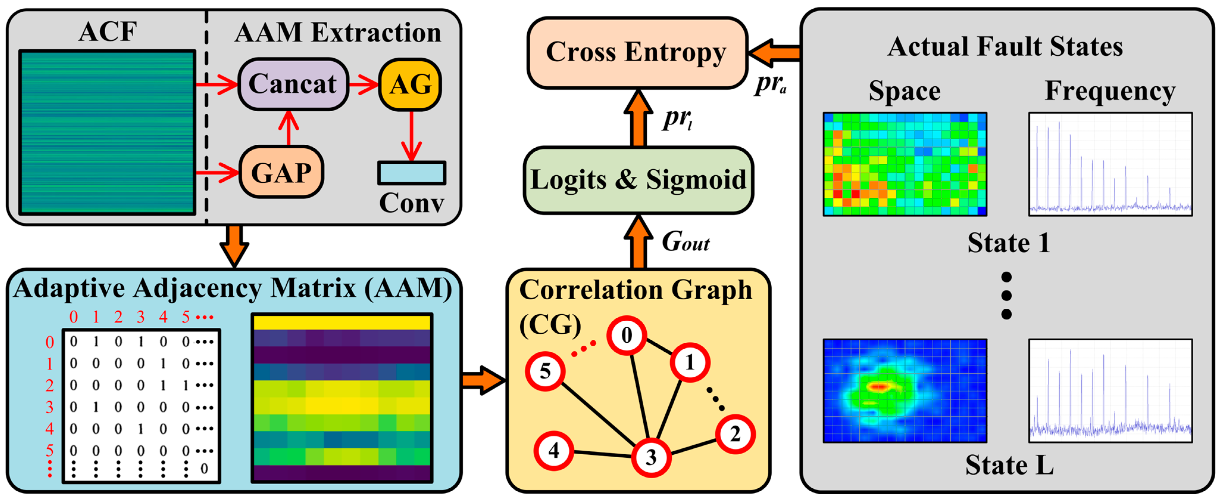
The ACF processed by the attention module has more prominent and clear primary information, which is further used to establish a PCB failure diagnosis model by combining association graph and convolution operation with AGCN. Then, AGCN adaptively captures the correlation between data nodes by learning the data relationships of the current input features and forms an adaptive adjacency matrix (AAM) that can be further analyzed using convolution operations to characterize the intrinsic relationships of the data. In Figure 5, this article combines ACF with the global vector of ACF to form a global ACF (AG), where AG is a feature matrix that contains both local and global features of the current data in AG by adding the global pooling can reflect the overall macro behavior of ACF. This splicing process can make ACF consider the impact of macro trends on the current feature state while retaining feature local characteristics, thereby making the model features more comprehensive and further improving the model’s generalization ability. Furthermore, the algorithm can perform convolution on each input of different AGs and normalize the data using the Sigmoid function to obtain AAM that describes data relationships and can follow data changes. The specific construction process of ADM is shown in the following equation:
A A M = S i g m o i d W C A G = S i g m o i d W C C o n c a t A C F , G A P A C F
where W C is the process matrix of the convolution operation. In Figure 5, AAM is an adaptive description that can continuously abstract relationships with new data through network training. It describes the correlation between data nodes and structures in a correlation graph (CG). This article takes CG as the description object of AGCN, providing more flexibility and diversity for the model. The specific calculation formula for the output data OAF of AGCN based on AAM is as follows:
O A F = R e L U A C F · A A M · W A
where W A is the weight matrix, R e L U x = m a x 0 , x .
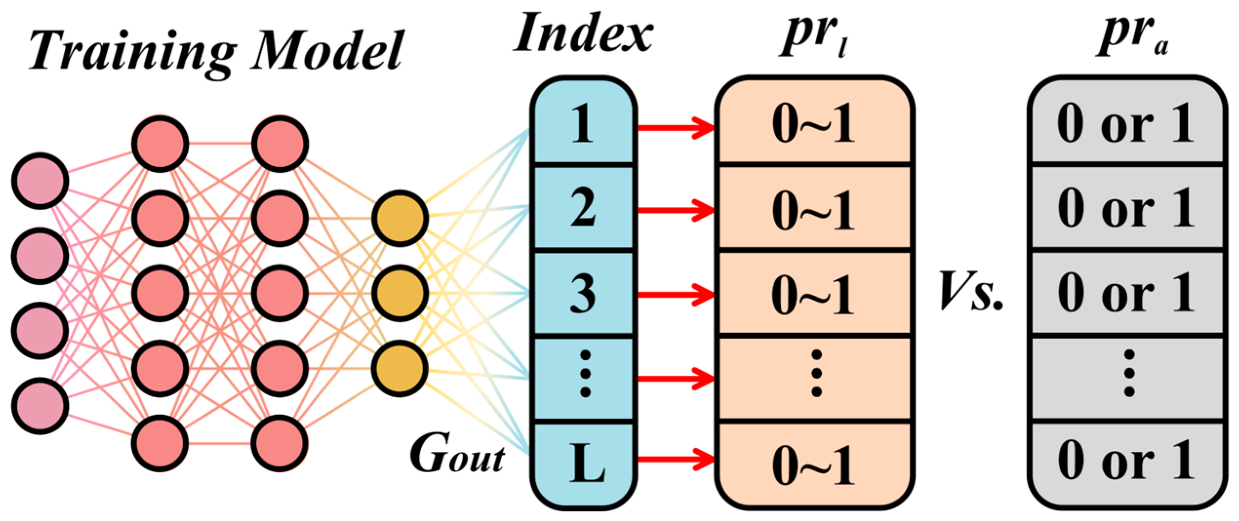
In order to quantify the judgment of PCB failure types by the training model, this paper adopts binary sequences as labels to store various failures of PCB. As shown in Figure 6, the output label takes the total number of PCB failures that need to be considered as the total number of bits in the binary label so that multiple PCB failures can be stored in different label bits. In order to further determine the failure type of PCB, this paper uses the Logit function combined with the Sigmoid function to perform probability operations on the tensor output by the model at each binary bit. The formulas for the Logit function and Sigmoid function here are as follows:
p o l = L o g i t G O U T = W O G O U T + b o p r l = s i g m o i d ( p o l ) = 1 1 + e p o l
where W O and b o are the weight matrix and bias vector of the Logit function, and p r l is the probability value containing feature information, l = 1 , , L . It is not difficult to find that the output of all binary bits is between 0 and 1.
In Figure 6, this article creates a set of actual labels p r a corresponding to the predicted labels by setting the number on the failure binary bit to 1 and vice versa; 0 on another set of binaries. Since the indices for different failure types on the two labels are the same, the cross-entropy function can be directly used to calculate the Loss value as the feedback error parameter for training the network. The specific cross-entropy function is as follows:
L o s s = 1 L · l = 1 L p r a · log p r l + 1 p r a · log 1 p r l
The cross-entropy loss function is chosen in this paper based on its applicability and wide application in multi-label classification tasks. First, the cross-entropy loss function can effectively handle binary multi-label classification problems, ensuring the model can optimize each label independently. Secondly, the model output layer uses a sigmoid activation function to convert the predicted value of each label into a probability distribution. The cross-entropy loss function can match this probability form well, providing an accurate gradient signal and optimizing the model’s log-likelihood. In addition, the cross-entropy loss function has good numerical stability when dealing with multi-label tasks, which can accelerate the convergence of the training process. Therefore, choosing the cross-entropy loss function can ensure the performance and training efficiency of the model.
In Figure 7, the entire PCB failure diagnosis algorithm will complete feature extraction, reinforcement, and training through three main modules: ResNet, SAM, and AGCN. ResNet dramatically enhances the depth of the network through residual blocks, thereby achieving refinement and compression of input data. SAM will supervise and extract more effective feature information through the self-attention mechanism. AGCN will establish a mapping relationship between features and failure types based on the adaptive correlation between features. The overall algorithm architecture is interconnected, aiming to achieve the extraction and mapping of deeper data information.

4. Actual Experimental Verification

In order to verify the feasibility and practical diagnostic performance of the PCB failure diagnosis algorithm (SRA) established by combining SRF features with the SAM and AGCN model, this paper designs and debugs a dual-phase amplitude boosting circuit (DPAB) that can manually set failures. DPAB, as an RF circuit that can generate biphasic signals, can subtract two RF signals with opposite phases to cancel out common mode noise and improve signal transmission capability. Therefore, this circuit can be widely applied in the aerospace field’s wireless communication and radar remote sensing systems.

4.1. Experimental Design

Figure 8a is a schematic diagram of the cross-sectional distribution of an aircraft electronic system, which illustrates that the communication module where the DPAB is located can be installed in the cockpit, cabin network module, and antenna. In Figure 8b, DPAB is an RF circuit with various typical PCB failures such as phase reversal, phase holding, power amplification, power state, circuit matching, and load state, making it an ideal experimental object. In Figure 8c, in order to obtain a pair of inverted voltage signals from the single-phase RF input terminal RF_in, this paper uses CD74HC4049 and CD74HC4050 to form a pair of two-phase drive circuit groups (DPC). The input and output terminals of the circuit are equipped with load resistors to ensure stable signal voltage, and the DC paths of both chips are designed with bypass capacitor groups C b 1 and C b 2 to ensure the purity of the DC path. In Figure 8d, this article adds two power amplifier circuits (PA) with AFT05MS003N N-type field-effect transistors as power cores to the DPC backend to boost the signal power and further filter out AC stray signals to increase signal availability. This article adds four isolation capacitors, C 23 , C 41 , and C 20 , C 39 to the connection ports of DPC and PA to provide path filtering while ensuring that DC signals will not be injected into measuring instruments and other circuits during debugging and setting of mismatch failures. PA adopts a multi-level LC matching mode to design the end matching circuit and uses bypass capacitor groups C b 3 , C b 4 , and C b 5 , C b 6 to ensure the purity of the DC port of the power amplification circuit.

4.2. Test Platform Construction

In actual circuit systems, changes in each functional module of DPAB may cause inconsistencies in the overall circuit performance, so PCB failure diagnosis algorithms need to identify various abnormal states when detecting and repairing DPAB accurately. For a low-frequency circuit, failures are usually caused by the on–off of the AC/DC path and abnormal load, while for a high-frequency circuit, abnormal matching of circuit ports may also lead to some functional failures. Based on careful consideration of typical failures in RF circuits, this article sets up jumper blocks on DPAB that can simulate various failures in the circuit and set up mismatch paths and multiple load paths to provide a diversity of failures for the circuit. The opening and closing of the jumper block can easily simulate the common on–off state changes in the circuit. However, to further simulate the load performance degradation that may occur in some ordinary PCBs and the matching problems that may occur in RF PCBs, it is necessary to set up additional abnormal paths to simulate such problems. This paper uses multiple jumper blocks to control different load paths and mismatch paths to achieve this process, that is, selectively connect and disconnect the jumper blocks when simulating normal and abnormal paths. These performance abnormalities will not cause apparent failure of the PCB functional modules, but the performance does not usually meet expectations when the PCB is working. In particular, matching problems will not cause direct changes in the primary frequency but may cause changes in the impedance of different frequencies, thereby affecting the change in the pass rate of the required frequency signal. Therefore, such performance degradation problems should be seriously considered, especially in precision systems such as aerospace electronic systems, where any potential functional degradation may be amplified in the operation of related functional modules. It is worth noting that this article does not limit the circuit to having only a single type of failure but allows the circuit to have multiple types of failures simultaneously, which is also in line with the actual situation of failure circuits in practice. This paper effectively simulates typical problems such as fundamental on–off, matching, and load anomalies in PCB and their combination problems. Table 1 describes all types of failures in this article and their corresponding setting methods. All multiple failures involved in the experiment are composed of single failure combinations from the table. The failure settings are not unique, but the settings in this article cover various typical situations and can verify the algorithm’s feasibility enough.
In Figure 9, this article adjusts the measurement distance between the DPAB and the EMSCAN EMxpert EHX [42] electromagnetic scanner by attaching silicone patches with different diameters and heights of 5 mm and 2 mm at the four corners of the DPAB front surface. This standard-sized silicone gasket can effectively control the measurement spacing when collecting signals to flexibly obtain more magnetic field data under different standard distance measurements according to experimental requirements. The overall test adopts a digital adjustable DC power supply, signal analyzer N9010B [43], and personal computer to achieve circuit power supply and measurement data acquisition.

4.3. Experimental Environment Assessment

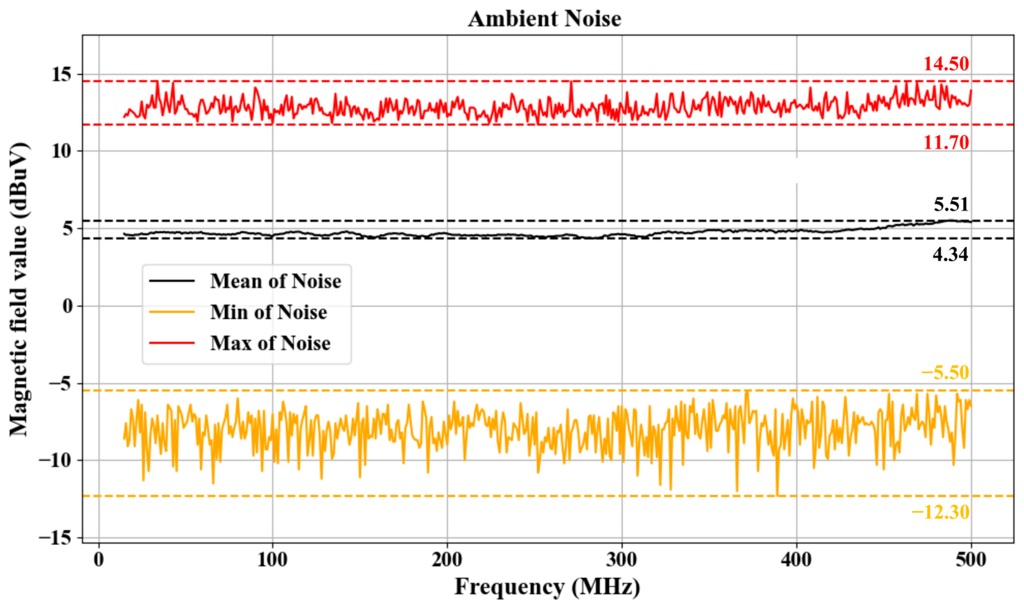
As a non-contact PCB failure diagnosis algorithm based on electromagnetic measurement methods, the measuring instrument can effectively collect radiation magnetic field data from the PCB. However, other devices and instruments in the environment usually have some noise and are collected by measuring instruments. In order to ensure the effectiveness and reliability of the magnetic field data used by the algorithm, the experiment considered the influence of environmental noise on the measurement data. As shown in Figure 10, based on the measurement platform shown in Figure 9, this article conducted 30 environmental magnetic field scanning tests with the PCB removed and plotted the mean, minimum, and maximum values of interference noise on spatial measurement points at each measurement frequency. It is not difficult to find that the distribution of the three typical values of interference noise is relatively stable, which means that environmental interference is relatively stable and there is no noticeable distortion. At the same time, the maximum value of environmental noise that affects practical magnetic field data does not exceed 14.5 dBuV, which means that all magnetic field data above this noise can reflect the working state of the PCB.
In order to ensure the accuracy and effectiveness of the measurement, this article adopts a threshold ε t h denoising method to ensure that the data have high PCB features. This method preserves magnetic field data H that is bigger than the maximum value of environmental noise. Otherwise, the value is set to . The specific filtering method is as follows:
H = H   , H ε t h , H < ε t h
All experimental data in the article will be preprocessed using this filtering scheme before input into the algorithm, which greatly ensures the validity of the original data and the reliability of the algorithm validation process.

4.4. Algorithm Setting and Experimental Data Analysis

The magnetic field data in this paper is derived from near-field scanning, which is mainly used to ensure the integrity of the radiation characteristics of the PCB fully. According to the magnetic flux source radiation formula provided in the literature [44] as follows:
H & = I m z l cos θ e j k 0 r j 2 π ω μ r 3 1 + j k 0 r r + I m z l sin θ e j k 0 r j 4 π ω μ r 3 1 + j k 0 r k 0 2 r 2 θ
where I m z l is the magnetic current source, ε is the dielectric constant of the medium, k 0 = ω ε μ is the wave number, ω is the angular frequency of the magnetic field, μ is the medium’s permeability, r the distance between the magnetic field and the source of the magnetic current. It can be found that when the original factory measurement is performed, k r 1 , then the radiation formula only retains the main items shown below:
H & j k 0 ε I m z l sin θ e j k 0 r 4 π r
where ε is the wave impedance. The signal processing module of the PCB usually radiates weakly, while the power module usually radiates strongly. In the far-field case, many weak signals will be lost, thereby weakening the characterization ability of the characteristics. In addition, the signal in the far-field case is weaker than that in the near-field case, which will increase the interference of external radiation and is not conducive to generating practical characteristics.
In order to establish a comprehensive PCB failure diagnosis verification experiment in the near-field, this paper combines all single failures in Table 1 with a maximum of 4 failures co-occurring. Moreover, at two measurement heights of 6 mm and 8 mm, 86 PCB magnetic field states were collected, and 10–20 random measurements were taken for three spatial dimensions in each state (the total of 2866 samples). The experimental scanning frequency range is determined to be 15–500 MHz, with resolution bandwidth (RBW) of 1 MHz (scanning interval 1 MHz). The validation experiment has sufficient randomness and typicality, covering typical issues such as DPAB on–off and performance degradation under single and multiple failure conditions.
In order to establish a specific SSA algorithm in conjunction with experiments, this paper uses eight batches to divide the samples into a ratio of 8:2 to establish a random data training set and validation set. Channel × Width × Height = 8 × 224 × 224 is used as a data-parallel training input to normalize the Z-score normalization module with a mean and standard deviation of 0.5. The optimizer uses second-order momentum Adam [45], with a learning rate of l r = 2 × 1 0 5 , decay parameter of β 1 , β 2 = 0.9,0.999 , and stability constant ε = 1 0 8 .
Based on the above PCB failure set collection and actual model parameter setting scheme, this paper uses five levels of feature networks (FN) in SRA, namely ResNet18, ResNet34, ResNet50, ResNet101, and ResNet152, to extract the magnetic field features of PCBs, and compare the performance differences that may occur when different levels of FN are combined with AGCN. ResNet18 and ResNet34 use a basic block containing two 3 × 3 convolutional layers, while ResNet50, ResNet101, and ResNet152 use a bottleneck residual block containing three convolutional layers, namely 1 × 1, 3 × 3, and 1 × 1. This article uses multiple quantitative indicators to measure the comprehensive performance of the model, including Overall Precision (OP), Per Class Precision (CP), Overall Recall (OR), Per Class Recall (CR), Overall F1 Measure (OF1), Per Class F1 Measure (CF1), Accuracy (ACC), Mean Average Precision (MAP) [46]. The specific calculation formulas for each evaluation indicator are as follows:
O P = i = 1 N N i c i = 1 N N i p   C P = 1 C i = 1 N N i c N i p   O R = i = 1 N N i c i = 1 N N i g   C R = 1 C i = 1 N N i c N i g O F 1 = 2 × O P × O R O P + O R   C F 1 = 2 × C P × C R C P + C R A C C = i = 1 N N i c N   M A P = i = 1 N A P i N
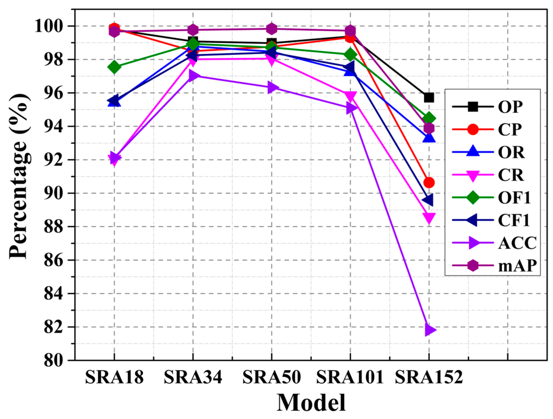
where N i c is the number of correctly predicted i-th failures, N i p is the number of predicted j-th failures, N i g is the actual number of j-th failures, A P i is the average accuracy of i-th failures, C is the number of failures to be predicted, and N is the total number of samples. From the experimental results, it can be seen that different combinations of ResNet and AGCN can accurately diagnose multiple failures in PCB.
Figure 11 uses a line chart to describe the indicators in Table 2. It can be seen that the values of each indicator are relatively high when the model is equipped with different FN, but there is no precise quantitative evaluation in different models.
In Figure 12, to qualitatively measure the comprehensive performance of the model, this paper compares the eight indicator values of different models as 8-dimensional spatial coordinate points with 100% Euclidean distance. The formula for calculating Euclidean distance is as follows:
E D = i = 1 n p i p o 2
where p i is the indicators, p o is the 100%, i = 1,2 , 3 , , 8 .
From the experiment results, the RestNet34 as the feature extraction network can achieve optimal model performance, which further illustrates that the more complex the feature extraction network, not must be the better. For PCB diagnosis problems with multiple failures, a suitable network layer and structure are necessary to extract more appropriate failure features. Based on the optimal feature extraction network, the algorithm independently calculated the individual accuracy (IAC) for the eight failures in Table 1 and achieved results of 100%, 99.30%, 99.65%, 99.65%, 100%, 99.65%, 98.78% and 99.30%.
I A C n = N n c N n
where N n c is the number of correctly predicted n-th failures, N n is the total number of n-th failures, n is the state numbers in Table 1, and n = 1,2 , , 8 . This result demonstrates that the algorithm has a high recognition accuracy for each failure. In addition, based on the optimal feature extraction network, this paper further evaluates the contribution of adding AGCN to the model’s overall performance. It directly compares failure diagnosis performance using ResNet by removing AGCN, obtaining the OP, CP, OR, CR, OF1, CF1, ACC, and MAP at 97.28%,94.89%, 98.47%, 97.23%, 97.87%, 96.05%, 94.41%, and 99.19%. Referring to the performance indicators of SRA34 in Table 2, AGCN has achieved an overall improvement of 1.80%, 3.61%, 0.31%, 0.78%, 1.06%, 2.20%, 2.62%, and 0.58% in OP, CP, OR, CR, OF1, CF1, ACC and MAP compared with ResNet, which is very precious in diagnosing multiple failure problems.
The experiment shows that it is different from the traditional EMC problem location method provided in the EMSCAN EMxpert EHX user manual. Furthermore, this paper uses a powerful neural network method to apply the data collected by the instrument more efficiently to analyses. Specifically, the traditional EMC problem detection determines the location and frequency of the PCB failure by subtracting the detection data from the normal state data and determining whether there is data exceeding the threshold in the spectrum difference in each spatial measurement point. With the help of the magnetic field scanning instrument’s powerful spatial and frequency scanning capabilities, this paper sets and radiates the magnetic field of different PCB failures, establishing a set of data sets of failures considered by the PCB. On this basis, the proposed SRA algorithm is used to realize the learning and training of the data set efficiently and further completes the rapid diagnosis of PCB multiple failures more objectively and automatedly. This point also highlights the significance of this paper, which can effectively eliminate the judgment result deviation caused by the different operator experience or measurement standards during diagnoses using the traditional method. In other words, this paper further utilizes the inherent characteristics of the data more effectively. It effectively uses the objective knowledge learned by the algorithm to comprehensively discover each collected data and the fast reading of objective non-destructive diagnosis of multiple PCB failures.

5. Discussion

5.1. Discussion on the Main Experimental Results of SRA

In this study, the non-contact PCB failure diagnosis algorithm based on a self-attention graph neural network demonstrated exceptional performance, particularly in multi-failure scenarios where its detection capabilities were significantly enhanced. The experimental results revealed that using ResNet34 as the feature extraction network yielded outstanding results across multiple vital metrics, achieving 99.08%, 98.50%, 98.78%, 98.01%, 98.93%, 98.25%, 97.03%, and 99.77% for OP, CP, OR, CR, OF1, CF1, ACC, and MAP, respectively. These results highlight the critical role of the network structure in effective PCB failure feature extraction. Notably, although more complex networks may offer increased feature extraction capacity, the experiments showed that complexity does not always directly correlate with performance. The strong performance of ResNet34 suggests that selecting the appropriate network depth and structure is crucial for efficient failure diagnosis.
Additionally, the study demonstrated the significant contribution of the Adaptive Graph Convolutional Network (AGCN) through comparative experiments. When AGCN was integrated with ResNet34, the model’s performance saw notable improvements, with increases of 1.80%, 3.61%, 0.31%, 0.78%, 1.06%, 2.20%, 2.62%, and 0.58% in OP, CP, OR, CR, OF1, CF1, ACC, and MAP, respectively. These improvements further validate AGCN’s advantages in complex failure detection tasks, enhancing model accuracy and adaptability to diverse failure modes. AGCN optimized the feature extraction process, making the model more precise and efficient in handling multi-failure diagnosis scenarios.
Moreover, the proposed algorithm shows strong potential in aerospace applications and provides a reference solution for other high-reliability industrial uses. The algorithm’s ability to achieve high accuracy across various metrics underscores its broad applicability, particularly in diagnosing different PCB failures. Furthermore, the non-contact failure detection method improves flexibility and safety in the diagnostic process, offering enhanced possibilities for rapid and precise PCB failure detection.

5.2. Comparison of SRA and Mainstream Diagnostic Methods

The experimental results in this paper have fully verified that the SRA algorithm has very effective PCB failure diagnosis performance when combined with ResNet, SAM, and AGCN. In recent years, various deep learning models have been applied to failure detection, each with unique strengths, limitations, and applicable background. To fully highlight the advantages of the proposed SRA, this section compares it with widely used models such as Extreme Learning Machine (ELM), YOLO, and Transformer [47,48,49]. These models represent different approaches to feature extraction, attention mechanisms, and failure detection strategies, which makes them relevant benchmarks for evaluating our method.
As a linear output network architecture with few parameters based on the gradient descent algorithm, ELM has high-speed network training capabilities and is easy to build. However, the hidden layer of ELM is susceptible, and the output is a linear mapping relationship, which makes it have high requirements for initialization data and the number of nodes, making it difficult to ensure its reliability for complex problems such as PCB failure diagnosis based on magnetic field data containing complex physical field information. On the contrary, SRA uses its deeper network stacking and self-attention mechanism to achieve more complex local and global failure feature extraction and mapping.
As a target detection method, YOLO performs excellently in solving the positioning task of specific targets. However, its implementation often requires manual box marking of different targets in the sample, which makes the preprocessing workload of YOLO modeling greater than that of SRA. In addition, the research of SRA is based on magnetic field data, so using YOLO requires box marking of magnetic field data, which will be very difficult to achieve. Because YOLO mainly solves the problem of visual target detection that people can directly understand, and there is a physical mapping relationship between electromagnetic data and PCB, it is difficult to directly mark the magnetic field area corresponding to the failure of PCB itself based on subjective ideas.
Transformer architecture is widely used in various classification and detection tasks as a self-attention mechanism with superior performance. Undeniably, Transformer has a very high accuracy and excellent logical framework. However, its implementation depends on three fundamental matrices: Query, Key, and Value, plus the position encoding and global attention structure of the sample, and its computational cost is greater than that of SRA. In contrast, the SAM structure in SRA with the same function is more straightforward, and AGCN can also more easily parse the relationship between data points.
The ResNet + SAM + AGCN framework in SRA thoroughly explains the advantages of deep feature extraction, attention mechanisms, and graph-based processing. It can achieve relatively simple network complexity based on fully considering the correlation between data and achieving excellent diagnostic performance in the PCB failure diagnosis problem studied in this paper.

6. Conclusions

This article mainly describes a non-contact PCB failure diagnosis algorithm based on a self-attention graph neural network, which includes the specific principles and implementation methods of feature extraction network, self-attention mechanism, and adaptive GCN. This article solves the problem of PCB multi-failure diagnosis, which is of concern in the aerospace field. By using non-contact near-field measurement methods to obtain scalar magnetic fields, the health status of PCBs can be determined, enriching the solutions for rapid PCB detection. Regarding the proposed PCB diagnostic algorithm, this article quantitatively analyzes the performance of the feature extraction network and SRA algorithm through an actual experimental design. It ultimately achieved actual results of 99.08%, 98.50%, 98.78%, 98.01%, 98.93%, 98.25%, 97.03%, and 99.77% on multiple indicators including OP, CP, OR, CR, OF1, CF1, ACC, and MAP, respectively. The actual testing performance of the overall algorithm is relatively excellent, providing an effective solution for PCB failure diagnosis in the aerospace field. This paper combines the ResNet feature extraction model, self-attention feature enhancement model, and adaptive convolutional graph neural network training model to provide a new solution to the PCB multi-failure diagnosis problem in avionic systems. In the future, other forms of features can be combined to establish a multimodal feature fusion algorithm to expand the scope of application of the algorithm.

Author Contributions

Conceptualization, C.L. and M.F.; methodology, C.L., M.F. and H.Y.; software, C.L.; validation, C.L. and M.F.; formal analysis, C.L.; investigation, C.L. and H.Y.; resources, C.L. and M.F.; data curation, C.L. and H.Y.; writing—original draft preparation, C.L.; writing—review and editing, C.L., M.F. and H.Y.; supervision, M.F. and H.Y.; project administration, C.L.; funding acquisition, M.F. and H.Y. All authors have read and agreed to the published version of the manuscript.

Funding

This research was supported by the National Natural Science Foundation of China (62473024 and 62073013), the 5720 Factory and Beihang Science and Technology Cooperation Project, and the Fundamental Research Funds for the Central Universities and China Scholarship Council.

Data Availability Statement

Data are unavailable due to privacy or ethical restrictions.

Conflicts of Interest

The authors declare no conflict of interest.

References

  1. Davis, M.E. Technology Innovation Continues to Drive Aerospace Electronic Systems Development. IEEE Aerosp. Electron. Syst. Mag. 2023, 38, 14–20. [Google Scholar] [CrossRef]
  2. Zheng, Z.X.; Guo, J.; Gill, E. Onboard Mission Allocation for Multi-Satellite System in Limited Communication Environment. Aerosp. Sci. Technol. 2018, 79, 174–186. [Google Scholar] [CrossRef]
  3. Xu, J. Research on the role of new electronic information technology in the development of modern avionics equipment. In Proceedings of the 2019 International Conference on Cloud Computing and Information Science, 2019 International Conference on Cloud Computing and Information Science, Shenyang, China, 27–29 December 2019. [Google Scholar]
  4. Saemi, F.; Benedict, M. Brushless DC Motor Sizing Algorithm for Small UAS Conceptual Designers. Aerospace 2024, 11, 649. [Google Scholar] [CrossRef]
  5. Reid, S.J.; Perez, R.E.; Jansen, P.W. Hybrid electric aircraft design with optimal power management. Aerosp. Sci. Technol. 2024, 154, 109479. [Google Scholar] [CrossRef]
  6. Cardone, L.M.; Petrone, G.; Rosa, S.D.; Franco, F.; Greco, C.S. Review of the Recent Developments About the Hybrid Propelled Aircraft. Aerotec. Missili. Spaz. 2024, 103, 17–37. [Google Scholar] [CrossRef]
  7. Zhang, Q.Y.; Norman, P.; Burt, G. Design Rules to Establish a Credible More-Electric Engine Baseline Power Architecture Concept. IET Electr. Syst. Transp. 2023, 13, e12076. [Google Scholar] [CrossRef]
  8. Wang, H.L.; Deng, J.Q.; Zhang, L.Y.; Bao, Q.L.; Mao, Y. Enhanced disturbance observer-based hybrid cascade active disturbance rejection control design for high-precise tracking system in application to aerospace satellite. Aerosp. Sci. Technol. 2024, 146, 108939. [Google Scholar] [CrossRef]
  9. Levchenko, I.; Xu, S.; Teel, G.; Mariotti, D.; Walker, M.L.R.; Keidar, M. Recent progress and perspectives of space electric propulsion systems based on smart nanomaterials. Nat. Commun. 2018, 9, 879. [Google Scholar] [CrossRef]
  10. Fkirin, M.A.; Khira, M.A.-E. Enhanced Antenna Positioning Control System Using Adapted DC Servo Motor and Fuzzy-PI Controller. IEEE Access 2023, 11, 102661–102668. [Google Scholar] [CrossRef]
  11. Ren, J.; Ji, X.; Han, L.; Li, J.; Song, S.; Wu, Y. Direct Closed-Loop Control Structure for the Three-Axis Satcom-on-the-Move Antenna. Aerospace 2024, 11, 659. [Google Scholar] [CrossRef]
  12. Heltzel, S.; Cauwe, M.; Bennett, J.; Rohr, T. Advanced PCB technologies for space and their assessment using up-to-date standards. CEAS Space J. 2023, 15, 89–100. [Google Scholar] [CrossRef]
  13. Duzellier, S. Radiation effects on electronic devices in space. Aerosp. Sci. Technol. 2005, 9, 93–99. [Google Scholar] [CrossRef]
  14. Ji, M.M.; Zhi, S.B.; Shi, J.B.; Wu, Q.; Huang, Z.Q.; Xie, P.F. Research on High Reliable Aerospace Secondary Power Supply Based on Resonant Reset Forward Converter. In Proceedings of the 3rd International Conference on Electrical Engineering and Control Technologies, Macau, Macao, 16–18 December 2021; pp. 8–13. [Google Scholar]
  15. Aliparast, P. Design and implementation of a high efficiency RF power amplifier for S-band telemetry subsystems. Int. J. Electron. Commun. 2016, 70, 1311–1320. [Google Scholar] [CrossRef]
  16. Chang, D.; Yang, B.; Lv, W.; Huang, J. Research on the Aerospace Mechatronic Servo System’s Digital Production Line Construction. In Proceedings of the 2021 4th World Conference on Mechanical Engineering and Intelligent Manufacturing (WCMEIM), Shanghai, China, 12–14 November 2021; pp. 311–315. [Google Scholar]
  17. Marcy, H.T. Parallel circuits in servomechanisms. Electr. Eng. 1946, 65, 1128. [Google Scholar] [CrossRef]
  18. Qian, J.Y.; Liu, M.; Xia, F.; Bai, Y.F.; Ou, D.X.; Kang, J.S. A Multimode Fusion-Based Aviation Communication System. Aerospace 2024, 11, 719. [Google Scholar] [CrossRef]
  19. Wileman, A.J.; Aslam, S.; Perinpanayagam, S. A road map for reliable power electronics for more electric aircraft. Prog. Aerosp. Sci. 2021, 127, 100739. [Google Scholar] [CrossRef]
  20. Yamaoka, A.; Hone, T.M.; Yamaguchi, K. 70% Efficient Dual-Input Doherty-Outphasing Power Amplifier for Large PAPR Signals. In Proceedings of the 2019 IEEE MTT-S International Microwave Symposium (IMS), Shanghai, China, 2–7 June 2021; pp. 311–315. [Google Scholar]
  21. Xie, D.; Lin, C.X.; Deng, Q.L.; Lin, H.J.; Cai, C.S.; Basler, T. Simple Vector Calculation and Constraint-Based Failure-Tolerant Control for a Single-Phase CHBMC. IEEE Trans. Power Electron. 2024, 1–14. [Google Scholar] [CrossRef]
  22. Jlassi, I.; Cardoso, A.J.M. A Single Method for Multiple IGBT, Current, and Speed Sensor Failures Diagnosis in Regenerative PMSM Drives. IEEE Trans. Emerg. Sel. Top. Power Electron. 2020, 8, 2583–2599. [Google Scholar] [CrossRef]
  23. Gou, B.; Xu, Y.; Xia, Y.; Deng, Q.; Ge, X. An Online Data-Driven Method for Simultaneous Diagnosis of IGBT and Current Sensor Failure of Three-Phase PWM Inverter in Induction Motor Drives. IEEE Trans. Power Electron. 2020, 35, 13281–13294. [Google Scholar] [CrossRef]
  24. Bhattacharya, A.; Cloutier, S.G. End-to-end deep learning framework for printed circuit board manufacturing defect classification. Sci. Rep. 2022, 12, 12559. [Google Scholar] [CrossRef]
  25. Park, J.-H.; Kim, Y.-S.; Seo, H.; Cho, Y.-J. Analysis of Training Deep Learning Models for PCB Defect Detection. Sensors 2023, 23, 2766. [Google Scholar] [CrossRef]
  26. Wagh, C.R.; Baru, V.B. Detection of Failurey Region on Printed Circuit Board with IR Thermography. Int. J. Sci. Eng. Res. 2013, 4, 1–4. [Google Scholar]
  27. Huang, W.B.; Wei, P. A PCB Dataset for Defects Detection and Classification. arXiv 2019, arXiv:1901.08204. [Google Scholar] [CrossRef]
  28. Lei, L.; Li, H.-X.; Yang, H.-D. Multi-scale Convolution-Based Probabilistic Classification for Detecting Bare PCB Defects. IEEE Trans. Instrum. Meas. 2023, 72, 1–8. [Google Scholar] [CrossRef]
  29. Stoynova, A.; Bonev, B.; Brayanov, N. Thermographic Approach for Reliability Estimation of PCB. In Proceedings of the 2018 41st International Spring Seminar on Electronics Technology (ISSE), Zlatibor, Serbia, 16–20 May 2018; pp. 1–7. [Google Scholar]
  30. He, W.; He, Y.G.; Li, B. Generative Adversarial Networks with Comprehensive Wavelet Feature for Failure Diagnosis of Analog Circuits. IEEE Trans. Instrum. Meas. 2020, 69, 6640–6650. [Google Scholar] [CrossRef]
  31. Chen, W.; Chinga, R.A.; Yoshida, S.; Lin, J.; Chen, C.; Lo, W. A 25.6 W 13.56 MHz wireless power transfer system with a 94% efficiency GaN Class-E power amplifier. In Proceedings of the 2012 IEEE/MTT-S International Microwave Symposium Digest, Montreal, QC, Canada, 17–22 June 2012; pp. 1–3. [Google Scholar]
  32. Marpaung, D.; Yao, J.P.; Capmany, J. Integrated microwave photonics. Nat. Photon 2019, 13, 80–90. [Google Scholar] [CrossRef]
  33. Kobayashi, Y.; Hori, M.; Noji, H.; Fukuda, G.; Kawasaki, S. The S-band GaN-based high power amplifier and rectenna for space energy transfer applications. In Proceedings of the 2012 IEEE MTT-S International Microwave Workshop Series on Innovative Wireless Power Transmission: Technologies Systems and Applications, Kyoto, Japan, 10–11 May 2012; pp. 271–274. [Google Scholar]
  34. Li, B.; Lei, M.Z.; Chen, M.; Zhang, L.Y. Electromagnetic Analysis of High-Frequency Digital Signal Processors. SpringerPlus 2016, 5, 1–14. [Google Scholar] [CrossRef]
  35. Wright, R.G. Spectroscopic electromagnetic analysis approach to non-contact circuit board test and diagnosis. In Proceedings of the 2015 IEEE AUTOTESTCON, National Harbor, MD, USA, 2–5 November 2015; pp. 173–180. [Google Scholar]
  36. Yu, S.W.; Cheng, J.Q.; Li, Z.C.; Liu, W.W.; Cheng, H.; Tian, J.G.; Chen, S.Q. Electromagnetic wave manipulation based on few-layer metasurfaces and polyatomic metasurfaces. ChemPhysMater 2022, 1, 6–16. [Google Scholar] [CrossRef]
  37. Spence, H.F. Printed circuit board diagnosis using artificial neural networks and circuit magnetic fields. IEEE Aerosp. Electron. Syst. Mag. 1994, 9, 20–24. [Google Scholar] [CrossRef]
  38. Yao, Z.; Pan, H. Failure diagnosis using magnetic image of PCB. In Proceedings of the 2012 UKACC International Conference on Control, Cardiff, UK, 3–5 September 2012; pp. 702–707. [Google Scholar]
  39. Jabbar, A.; Ramzan, R.; Siddiqui, O.; Amin, M.; Tahir, F.A. Wave discrimination at C-band frequencies in microstrip structures inspired by electromagnetically induced transparency. Sci. Rep. 2021, 11, 2983. [Google Scholar] [CrossRef]
  40. Jia, H.C.; Wan, F.Y.; Cheng, X.; Mordachev, V.; Chen, X.H.; Murad, N.M.; Ravelo, B. Electric near-field scanning for electronic PCB electromagnetic radiation measurement. Measurement 2024, 228, 114355. [Google Scholar] [CrossRef]
  41. Alaoui, N.E.B.; Boyer, A.; Tounsi, P.; Viard, A. New defect detection approach using near electromagnetic field probing of high density PCBAs. Microelectron. Reliab. 2018, 88–90, 288–293. [Google Scholar] [CrossRef]
  42. EMSCAN. EMxpert EHX User Manual. 2024. Available online: https://www.emcfastpass.com/test-equipment/wp-content/uploads/2016/10/EMxpert_EHX_User_Manual_v5.0.6.1-10.15.pdf (accessed on 12 October 2024).
  43. KEYSIGHT. N9010B EXA X-Series Signal Analyzer Multi-Touch. Available online: https://www.keysight.com/us/en/assets/7018-05049/data-sheets/5992-1256.pdf (accessed on 12 October 2024).
  44. Liu, C.X.; Yuan, H.W.; Lv, J.X.; Wang, Z.W.; Li, J.M.; Xu, H.; Zhou, H. A Calculation Method for Reconstructing Radiation State of PCB Using Known Magnetic Field Amplitude Information. IEEE Trans. Instrum. Meas. 2024, 73, 1–13. [Google Scholar] [CrossRef]
  45. Kingma, D.P.; Ba, J.L. Adam: A Method for Stochastic Optimization; Computer Science: San Diego, CA, USA, 2015. [Google Scholar]
  46. Chen, T.S.; Xu, M.X.; Hui, X.L.; Wu, H.F.; Lin, L. Learning Semantic-Specific Graph Representation for Multi-Label Image Recognition. In Proceedings of the 2019 IEEE/CVF International Conference on Computer Vision (ICCV), Seoul, Republic of Korea, 27 October–2 November 2019; pp. 522–531. [Google Scholar]
  47. Wang, X.W.; Zhao, Y.H.; Wang, Z.H.; Hu, N. An ultrafast and robust structural damage identification framework enabled by an optimized extreme learning machine. Mech. Syst. Signal. Process. 2024, 216, 111509. [Google Scholar] [CrossRef]
  48. Waikat, J.; Jelidi, A.; Lic, S.; Sopidis, G.; Kähler, O.; Maly, A.; Pestana, J.; Fuhrmann, F.; Belavić, F. First Measurement Campaign by a Multi-Sensor Robot for the Lifecycle Monitoring of Transformers. Energies 2024, 17, 1152. [Google Scholar] [CrossRef]
  49. Jia, Z.; Wang, S.D.; Zhao, K.; Li, Z.F.; Yang, Q.Q.; Liu, Z.B. An efficient diagnostic strategy for intermittent failures in electronic circuit systems by enhancing and locating local features of failures. Meas. Sci. Technol. 2023, 35, 3. [Google Scholar] [CrossRef]
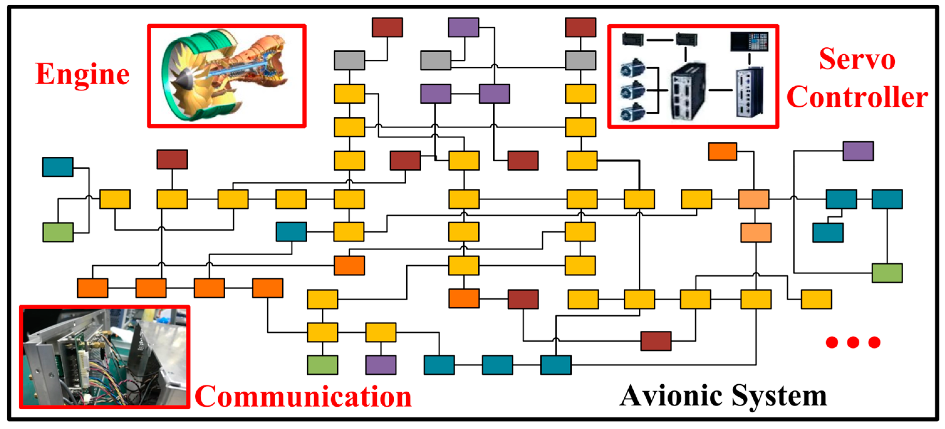
Figure 1. Schematic diagram of avionic system.
Aerospace 11 00864 g001
Figure 2. (a) Near field scanning of PCB electromagnetic field; (b) Dimensional reduction in the spatial plane; (c) Frequency spectrum of PCB; (d) Two-dimensional spatial frequency spectrum.
Aerospace 11 00864 g002
Figure 3. Residual module in ResNet.
Aerospace 11 00864 g003
Figure 4. Self-Attention feature enhancement mechanism.
Aerospace 11 00864 g004
Figure 5. PCB multi-failure diagnosis training model (AGCN).
Aerospace 11 00864 g005
Figure 6. Principle of multi-failure labels.
Aerospace 11 00864 g006
Figure 7. The information transmission relationship of the main modules.
Aerospace 11 00864 g007
Figure 8. (a) Schematic diagram of aircraft electronic system; (b) DPAB simulation model; (c) In-phase hold and phase reversal module; (d) Power amplifier circuits.
Aerospace 11 00864 g008
Figure 9. Actual experimental platform.
Aerospace 11 00864 g009
Figure 10. Ambient noise tested frequency spectrum.
Aerospace 11 00864 g010
Figure 11. Comprehensive parameters of the model in Table 2.
Aerospace 11 00864 g011
Figure 12. Euclidean distance of model.
Aerospace 11 00864 g012
Table 1. The DPAB single failure state setting method.
State NumbersThe Considered DPAB StatusesThe Involved Jumper Blocks
1RF input failureCut P5 and Cut P17
2DC power failureCut P1 or P3 or P7 or P16 or P19
3Input matching failure of PA1Cut P8 and Connect (Con) P15
4Output matching failure of PA1Cut P12 and Con P14
5Input matching failure of PA2Cut P20 and Con P25
6Output matching failure of PA2Cut P23 and Con P24
7Load failure of PA1Cut P10 and (Con P4 or Con P11)
8Load failure of PA2Cut P22 and (Con P18 or Con P21)
Table 2. SRA diagnostic parameters with different structure feature extraction networks.
ModelOPCPORCROF1CF1ACCMAP
SRA1899.79%99.85%95.42%92.05%97.55%95.55%92.13%99.67%
SRA3499.08%98.50%98.78%98.01%98.93%98.25%97.03%99.77%
SRA5098.98%98.76%98.47%98.05%98.72%98.41%96.33%99.83%
SRA10199.38%99.32%97.25%95.85%98.30%97.55%95.10%99.72%
SRA15295.72%90.64%93.28%88.58%94.48%89.60%81.82%93.89%
Disclaimer/Publisher’s Note: The statements, opinions and data contained in all publications are solely those of the individual author(s) and contributor(s) and not of MDPI and/or the editor(s). MDPI and/or the editor(s) disclaim responsibility for any injury to people or property resulting from any ideas, methods, instructions or products referred to in the content.