Abstract
The Oh-Park methodology was proposed to overcome the limitations of Steinberg’s theory for evaluating the structural safety of space-borne electronics and has been experimentally verified at the printed circuit board (PCB) specimen level for various types of electronic packages, such as ball grid arrays (BGAs), column grid arrays (CGAs), and small-outline packages (SOPs). However, it is necessary to validate the design methodology because the PCB mounted on the housing is affected by the elastic mode of the mechanical housing. In addition, although the validity of the existing theory based on critical strain has been verified for horizontally mounted structures, there are cases where PCBs are mounted vertically. Therefore, it is essential to consider the dynamic influence of the boundary conditions of mounted electronics. In this study, electronics specimens with corresponding boundary conditions were fabricated, and a fatigue-life test was performed. In addition, a structural analysis using Steinberg’s theory and the Oh-Park methodology was performed, and the results were compared with those of the fatigue-life test. The results showed that the analysis using the Oh-Park methodology accurately represented the test results, and the validity of the Oh-Park methodology for vertical electronics was verified experimentally.
1. Introduction
Space-borne electronics are exposed to extreme vibration environments during lift-off. The vibration environment consists of sine vibrations from the engine cut-off, shock load due to the separation events of the launch vehicle and satellite, and quasi-static load due to engine ignition and thrust [,,]. The acoustic noise acting on a satellite is transmitted to the electronics located inside the satellite structure in the form of random vibrations [,]. Random vibrations cause a relative displacement of printed circuit boards (PCBs) and the housing structure of the electronics. This can lead to the fatigue failure of solder joints, which are the mechanical and electrical interfaces between electronic packages and PCBs [,,,,,]. The failure of solder joints can lead to electrical malfunction or even mission failure. Therefore, it is of great importance to ensure the structural safety of solder joints because it is impossible for satellites to be repaired once they are launched into orbit. Therefore, a highly reliable structural design methodology is required for space-borne electronics.
In the aerospace sector, structural design has been widely used to evaluate the structural safety of solder joints based on Steinberg’s fatigue failure theory []. This theory enables the estimation of the allowable relative displacement between the PCB and the electronic package exposed to vibration excitation. Steinberg proposed the design criterion of 20 million cycles for random vibrations guaranteed when the maximum displacement does not need the allowable value estimated by Steinberg’s empirical formula. To date, space industries and organizations have actively utilized Steinberg’s theory to evaluate their electronics designs. One of the major advantages of Steinberg’s theory is that it allows the use of a simplified form of the finite element (FE) modeling technique for electronic packages using equivalent beams or rigid link elements []. The board displacement predicted based on the modeling technique was reasonably accurate for the design evaluation. The use of this technique reduced the time and effort required to construct the FE model of electronics with numerous packages compared with the detailed modeling technique that models the actual configuration of the package and solder joints in detail [,]. However, several recent studies have reported theoretical limitations of Steinberg’s theory [,,,]. First, the fundamental assumption of Steinberg’s empirical formula is that the four edges of a PCB are simply supported and have an ideal half-sine mode shape. This can lead to an inaccurate evaluation of electronics with complex mode shapes owing to the asymmetrical fasteners or stiffeners. Second, a relative position factor in Steinberg’s formula, which defines the position of the package on the PCB, renders the calculated margin of safety (MoS) excessively high as the package mounting area becomes closer to the edge of the PCB. Third, the design criterion of 20 million cycles for random vibration is too conservative compared with the total number of fatigue cycles accumulated on space-borne electronics from on-ground testing to launch. These limitations cause the mechanical overdesign of electronics, increasing their mass and volume.
Park et al. []. proposed a PCB critical-strain-based structural design methodology, called the Oh-Park methodology, to overcome the theoretical limitations of Steinberg’s theory. The Oh-Park methodology compensates for the limitations of Steinberg’s theory in the following ways. First, it evaluates the structural safety by the strain in the solder ball region of the PCB, which means that the PCB does not have to be an ideal half-sine mode shape. Second, this methodology eliminates the error-causing factors in Steinberg’s empirical formula by calculating the MoS based on the PCB strain instead of the board displacement to evaluate the structural safety of space-borne electronics. Third, the design criterion is estimated based on the total number of fatigue cycles for the electronics subjected to the on-ground tests and launch, thereby minimizing the overdesign of the electronics. To validate the Oh-Park methodology, PCB specimens with various packages and boundary conditions were fabricated to perform a fatigue-life test, and the results were compared and analyzed with the structural analysis results [,,].
The Oh-Park methodology includes not only a method for evaluating the structural safety of solder joints based on the critical strain of PCBs but also a simplified FE modeling technique that is efficient in terms of time and effort when performing structural analysis. Park et al. [,,]. proposed an optimal modeling technique for geometrical characteristics, such as the length of solder joints and number of solder balls, by performing trial-and-error studies for different numbers of nodes in highly integrated electronic package models, such as ball grid arrays (BGAs), column grid arrays (CGAs), and small-outline packages (SOPs). PCB specimens with electronic packages were fabricated, and fatigue-life tests were performed for various mounting locations of the electronic packages to verify the effectiveness of the methodology and simplified modeling method. The fatigue-life test results were compared and analyzed with the PCB strain-based structural analysis results using a simplified modeling technique. Thus, the effectiveness of the FE modeling technique and structural design methodology for a variety of highly integrated electronic packages was experimentally verified at the PCB specimen level.
In the aforementioned studies, the Oh-Park methodology was validated only at the PCB-specimen level. In addition, a housing structure was applied to protect the internal PCB for electronics used in the industrial field. In this case, the application of Steinberg’s theory led to inaccurate results when evaluating the structural safety of solder joints in electronic packages because PCBs exhibit complex mode shapes influenced by the elastic modes of mechanical housing []. Therefore, Park et al. [] performed fatigue-life tests on electronics with various types of packages mounted on a PCB under numerous boundary conditions to verify the effectiveness of the critical-strain-based methodology, including conditions where the elastic mode of the housing occurred. Furthermore, they compared the Oh-Park methodology-based structural analysis results with the test results.
Previous studies on the validation of this methodology have been performed for cases in which PCBs are mounted horizontally. However, it is common for PCBs to be vertically mounted in the housing when electronics are carried on a satellite []. Spaceborne electronics—especially those comprising numerous sub-modules or high-heat generation components—prefer the vertical mounting method on the satellite panel. This strategy improves the thermal control of electronics as the heat paths from sub-modules to the base panel are shorter compared to those mounted horizontally. Vertical electronics are subjected to severe bending behavior due to the boundary condition of being attached to a satellite panel with a single fixed end. Furthermore, they are more vulnerable due to the lack of contact surfaces that can reduce the bending behavior of the PCB out-of-plane direction. However, the structural design techniques for vertically mounted electronics have not been studied before. In vertical electronics, the complex mode shape due to the combination of the global bending mode and the local PCB mode can result in even larger errors. Therefore, it is essential to validate the application of the Oh-Park methodology for the structural design of electronics with vertically mounted PCB and its corresponding boundary conditions.
In this study, electronic specimens were fabricated in housing with a vertically mounted PCB to verify the effectiveness of the Oh-Park methodology under the aforementioned conditions. Additionally, fatigue-life tests were performed at different mounting locations of the electronic package. The MoS and time to failure (TTF), which were calculated using a simplified modeling technique for electronic packages and verified in a previous study, were compared with the fatigue-life test results. Furthermore, a structural safety evaluation using Steinberg’s theory was performed and compared with the fatigue-life test results, confirming that the critical strain-based Oh-Park methodology was more representative of the test results.
The remainder of this paper is organized as follows. Steinberg’s theory and the Oh-Park methodology for evaluating structural safety are presented in Section 2. The fatigue-life test results are described in Section 3. A structural analysis using simplified modeling techniques and validation of the Oh-Park methodology through a comparative analysis with the fatigue-life test results are presented in Section 4. Finally, the conclusions of this study are presented in Section 5.
2. Design Methodology
Steinberg’s fatigue failure theory has been widely used as a structural design technique for space-borne electronics since it was proposed in the 1970s. This theory calculates the maximum allowable displacement based on the relative displacement between an electronic package and a PCB board when the PCB is subjected to repetitive bending behavior in a random vibration environment. The empirical formula for the allowable displacement is derived by assuming that the four corners of the PCB board are simply supported and is calculated as follows:
where C denotes the package constant for the electronic package, and each electronic package has a different value depending on the layout of the solder balls and lead wires and the manner in which they are mounted on the PCB. For example, 1.0 for a dual-in-line (DIP) package, 2.25 for a leaded ceramic chip carrier package (LCCC), and 1.75 for a surface-mounted ball grid array. Here, t denotes the PCB thickness, r denotes the position factor of the electronic package on the PCB, L denotes the length of the electronic package, and d denotes the length of the PCB parallel to the package. The calculated MoS was used to evaluate the structural safety of the solder joints of the electronic package using the allowable displacement of the PCB, calculated using Equation (1), and the maximum displacement () of the PCB was derived from the structural analysis. The MoS was calculated as follows:
where the factor of safety (FoS) denotes the safety factor of the MoS, typically with values of 1.25, 1.5, and 2.0. The European Cooperation for Space Standardization (ECSS) rule specifies the minimum FoS value for each structure []. The MoS should always be greater than 0. A positive MoS value indicates that the solder joints of the electronic package will not fail within the design criterion of 20 million cycles.
Steinberg’s theory has theoretical limitations because it is derived from the fundamental assumptions mentioned above. Space-borne electronics have various boundary conditions owing to their complex fixation points and stiffeners. Consequently, they cannot have an ideal half-sine mode shape. Therefore, the value calculated using Equation (1) exhibited the following errors: complex mode shapes causing ambiguities for determining the d-factor, which represents the length of the PCB parallel to the package, resulting in positive or negative evaluations of the MoS value. The r-factor, which represents the position of the electronic package on the PCB board, could be overestimated for electronic packages closer to the edge of the PCB. This may cause inaccurate structural safety evaluations and lead to unnecessary increases in clamping forces or the use of additional stiffeners. Consequently, the accumulated thermomechanical fatigue life of solder joints can be reduced, and the volume and weight of space-borne electronics can be increased. Despite these theoretical limitations, Steinberg’s theory is still being actively applied. However, the need to develop highly reliable space electronic structural design techniques to design small, lightweight satellites is growing with the emergence of a new space paradigm.
Park et al. []. proposed the Oh-Park methodology to overcome the limitations of Steinberg’s theory and achieve fast and accurate structural safety evaluations based on the PCB strain. In this methodology, structural safety was evaluated using MoS calculations in the same manner as Steinberg’s theory but using and instead of , . is the critical value of the principal strain in the PCB in-plane direction, and is expressed as follows:
where denotes the allowable PCB in-plane strain, which is substituted by deleting the error-causing factor in Equation (1). is calculated as follows:
where denotes the strain rate of the PCB, which is the value of per unit time. represents the in-plane principal strain of the PCB. and are calculated as
respectively, where and denote the in-plane normal strains, and denotes the root mean square (RMS) value of the in-plane shear strain. is calculated using the RMS values of normal and shear strains based on the 3σ value of the Gaussian distribution of random vibration []. The RMS value is derived through FE structural analysis. Finally, based on the previously calculated and values, MoS is calculated as follows:
where DF denotes a factor that complements the FoS applied in conventional Steinberg’s theory to prevent the overestimation of the MoS. This factor is based on the calculated in terms of the actual fatigue accumulation instead of the design criterion of 20 million cycles. is derived based on Minor’s hypothesis that the accumulated damage to structure is linearly related to the stress or strain in the elastic region [].
where and denote the sums of the fatigue times in the electronics level qualification and satellite system level acceptance tests, respectively; denotes the sum of the fatigue time based on the fatigue experienced in the actual launch environment, which is equivalent to 4 min of fatigue exposure to the full acceptance level (−3 dB) []; denotes a safety factor for the TTF and is set to 4, which is recommended for metallic materials in the ECSS rule []; denotes the design criterion of 20 million cycles from Steinberg’s conventional theory; DF can be expressed as the exponent of the ratio between the fatigue life of 20 million cycles and actual fatigue life of the electronics; and b denotes the fatigue exponent of the solder material. The value of 6.4 for the Sn37-Pb63 solder, which is an experimental value calculated from the stress cycles (S-N) fatigue curve with a stress concentration factor of 2, is presented in Steinberg’s textbook [].
Park et al. [,,] proposed a simplified FE modeling technique using rigid link elements and a zero-dimensional (0D) lumped mass to reduce the time and effort required to perform a structural analysis using FE models. A 0D lumped mass is a method for simulating the mass of a physical system by assuming that it is concentrated at a single point, allowing electronic components to be implemented through connections to the nodes of the PCB board using rigid link elements. The number of nodal points in the modeling for the CGA, BGA, and SOP packages was determined through trial and error by considering the number and shape of the solder joints for each electronic package. The simplified modeling technique was based on substituting the electronic package with an equivalent 0D lumped mass that was modeled to be located at the package’s center of gravity (CoG). In addition, the solder joints were modeled as rigid link elements. This modeling technique has significant advantages in terms of time and effort compared with detailed modeling by avoiding the modeling of all package bodies and individual solder joints when performing iterative trial-and-error studies in the early electronics design phase.
PCBs are mounted on mechanical housing structures in space-borne electronics, and the elastic modes of the housing can affect the modes of the PCB. Therefore, it is essential to consider the dynamic behavior of the housing when evaluating the structural safety of electronic-package solder joints. In a previous study, Park et al. [] performed fatigue-life tests on PCBs with various electronic packages mounted in housing under different boundary conditions to experimentally validate the proposed methodology at the electronics level.
However, most electronics with a large number of modules or high-heat dissipation are designed in the form of vertical PCB modules and mounted on the external side of the spacecraft. Figure 1 shows a high-speed digital receiver unit (HSDRU) developed for a space-borne synthetic aperture radar, which is a typical example of electronics attached to a satellite in a vertical direction from the ground []. It is mounted vertically in a multilayered insulation (MLI) tent with a radiator outside the spacecraft panel owing to the electronics applying a field-programmable gate array (FPGA). It is a high-heat dissipation component owing to its high-speed signal processing operations; therefore, the electronic is mounted vertically so that the heat is radiated to deep space rather than conducted to the satellite.
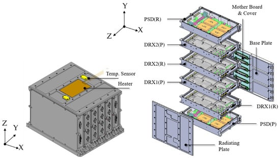
Figure 1.
Examples of electronics mounted vertically from the ground (HSDRU) [].
In the case of horizontally mounted electronics, the mounting surface acts as a rigid barrier, reducing the response level in the out-of-plane direction, which is the main direction of the bending behavior. In contrast, the vertical electronics mounting strategy has distinct differences from horizontal electronics in terms of the structural behavior of the launch environment. The out-of-plane vibration on the PCB is dominant in causing solder joint failure. In the case of horizontal mounting, the mounting surface of the electronics and the base panel surface are in contact. This means that the vibrational response of the electronics in the out-of-plane direction of the PCBs can be reduced due to the presence of the base panel, which acts like a mechanical barrier. In addition, a higher response reduction can be expected if thermal interface materials like thermal gap pads or Sigraflex layers are applied between the surfaces of the electronics and the base panel. On the other hand, in the case of vertical mounting, the out-of-plane direction of the PCB becomes equal to one of the in-plane directions of the electronics. This means that the vibration reduction caused by the base panel cannot be expected anymore. Additionally, the mode shape of the PCB becomes even more complex than in the horizontal mounting case due to the combination of the global bending mode of the sub-modules and the local modes of the PCBs themselves. This complexity in the combination of mode shapes is less likely in the horizontal mounting case. Figure 2 shows a difference between horizontally and vertically mounted electronics. Due to the characteristics described above, predicting the mechanical safety of the solder joint for the vertical mount case is far more difficult than for the horizontal mounting case. In this regard, it cannot be guaranteed that the Oh-Park methodology provides a reliable prediction of solder joint safety in the vertical mounting case for the electronics. Therefore, it is essential to validate the effectiveness of the Oh-Park methodology in vertically mounted electronics.
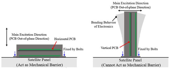
Figure 2.
Schematic representation of the difference between horizontally and vertically mounted electronics.
The analysis of vertical electronics is essential for the development of future electronics with highly integrated and high-heat dissipation components for advanced space missions. In this study, an electronics specimen with a corresponding boundary condition was fabricated to validate the Oh-Park methodology under a vertically mounted PCB boundary condition, and a fatigue-life test was performed. The test results were compared with the results of the structural analysis using Steinberg’s theory and the Oh-Park methodology.
3. Fatigue-Life Test of Electronics Specimens
An electronics specimen with a vertically mounted PCB and a single fixed-end boundary condition was fabricated to validate the effectiveness of the Oh-Park methodology. The specimen was intentionally designed to demonstrate the elastic bending behavior of the housing caused by the boundary condition, as shown in Figure 3. An FR-4, a composite composed of woven fiberglass cloth with an epoxy resin binder, was used to fabricate a PCB board with an area of 125 × 125 a thickness of 1.8 mm, and eight fixation points. The electronic package applied to the specimen was the plastic ball grid array (PBGA) 928 package (Amkor Co., Ltd., Tempe, AZ, USA), which was selected because it is considered vulnerable to failure in a launch vibration environment owing to its relatively large size and heavy weight (6.76 g) compared with typical packages. In addition, PBGA packages, which are BGA-type packages, are widely used in microelectronic packaging technologies owing to their advantages of low cost, high input/output density, and good electrical performance [,]. The specifications of the PBGA928 electronic package are listed in Table 1. As shown in Table 1, the PBGA928 package consisted of 928 solder balls made of Sn63-Pb37. A dummy package with a daisy-chain type was used to verify only the mechanical failure of the solder balls through fatigue-life testing.
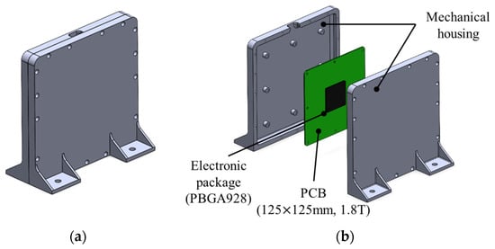
Figure 3.
Configuration of electronics specimen ((a) isometric view and (b) exploded view).

Table 1.
Specifications of the PBGA928 electronic package.
Figure 4 and Figure 5 show the package mounting locations for each case. In actual electronics, the relative positions of the fixation points and packages are diverse, which affects the fatigue life, depending on the mounting position of the package. To consider the impact of the boundary conditions between the package and fastening parts, specimens were created for the three different cases. Cases 1, 1-1, and 1-2 set the package at the center of the PCB, between the edge and center of the PCB, and closer to the edge of the PCB, respectively.
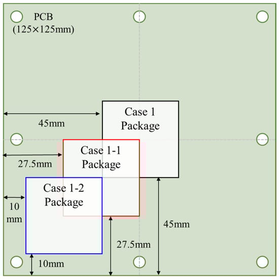
Figure 4.
Configuration of each PCB specimen according to package-mounting location.
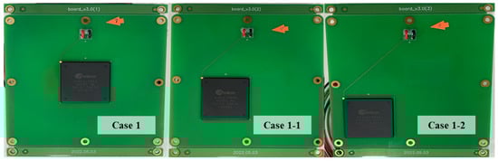
Figure 5.
Configuration of PCB for the fatigue-life test.
An example of a daisy-chain connection in the PBGA928 package is shown in Figure 6. The daisy-chain resistance measurement method was applied to detect the failure of the electronic package during the fatigue-life test. This method is useful for packages with many solder balls because it measures resistance by connecting all solder balls from a package in a single line. The measured resistance value increased if one solder ball was damaged, and failure could be detected in real-time during the test. The failure of solder joints occurred when at least 1.2 times the initial value of the daisy-chain resistance was detected five times in a row according to the IPC-9701A standard [].
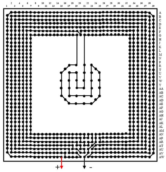
Figure 6.
Example of daisy-chain circuit for the PBGA928 package.
The fatigue-life test was performed with one fixed end so that the bending behavior could be accurately observed according to the boundary conditions of the specimen. The setup of the fatigue-life test is shown in Figure 7 and Figure 8. An integration jig was used to ensure that the specimens vibrated along the primary excitation axis, where the bending mode appeared. An interface was designed in the housing to connect the harness of the daisy-chain resistance measurements to the DAQ. Additionally, an accelerometer was attached to the integration jig to accurately measure and control the input PSD during random vibration excitation. The input-power spectral density (PSD) of the random vibration was 20 Grms at full level, as listed in Table 2, where Grms is the RMS value of acceleration, which represents the magnitude of vibration. The 20 Grms input level exceeds the vibration levels that electronics typically encounter in actual launch environments. However, to measure the failure time of the specimens in fatigue-life testing, a higher value was used to induce specimen failure.
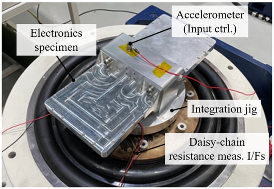
Figure 7.
Fatigue-life test setup for electronics specimens.
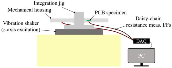
Figure 8.
Schematic of the fatigue-life test setup.
Table 2.
Specifications of random vibration input.
The resistance values measured through the daisy-chain were obtained using a data acquisition device (DAQ) (DAQ6510, Keithley Co., Ltd., Cleveland, OH, USA). The measurement accuracy of the DAQ was or less, and the sampling rate was set to 1.7 samples/s, which is considered to be suitable for detecting the failure of solder balls in real-time. The test was performed until the electronic package inside the housing satisfied the failure criteria of the solder joint. The TTF of the specimen in each case was measured by exciting the electronics with the input PSD described above. The TTFs in the fatigue-life test are listed in Table 3, and the daisy-chain resistance of the electronic package is shown in Figure 9. The test results showed that Case 1-1 was the first to fail at 37.75 s, followed by Cases 1 and 1-2 at 44 and 84.84 s, respectively. The above test results were used to validate the Oh-Park methodology for the boundary conditions, where the PCB was vertically mounted in the housing and affected by the bending behavior.
Table 3.
TTFs measured in the fatigue-life test.
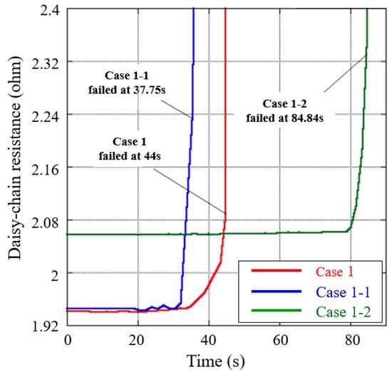
Figure 9.
Daisy-chain resistance of electronic packages.
4. Verification of Structural Design Methodology
A PBGA928 package, which is a BGA-type package with solder balls/columns arranged as a 2D array, was used in this study. The electronic package was implemented using simplified modeling techniques established by trial and error in previous studies [,,]. In addition, a rigid link element was used with nine nodal points, three constrained translational degrees of freedom (3 DoF), and a 0D lumped mass, as shown in Figure 10.
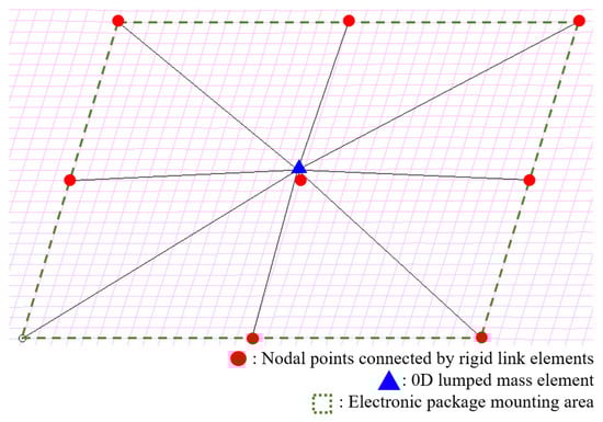
Figure 10.
Simplified modeling of the PBGA928 package.
For PCBs, 2D shell elements (Tri3, Quad4) were used to create a model with a smaller mesh density to limit the DoF of rotation and enable a more accurate prediction of the PCB strain compared to that of three-dimensional (3D) solid elements. The mesh size of the electronic package mounting area was set to 1.35 mm, which was the length of the package body divided by the number of solder balls on one side of the package. The remainder of the PCB was meshed with a size of 1.5 mm. The housing structure was constructed using Tet10, a 3D solid element in the shape of a tetrahedron with 10 nodes. In the case of the boundary condition of the test specimen, the housing structure was integrated with a jig, and the bolting points were modeled by applying a rigid body element (RBE2) that constrained the 6 DoF of translation and rotation. An example of the FE modeling of electronics (Case 1) is shown in Figure 11, where modal and random analyses were performed to evaluate the structural safety of electronics based on the Oh-Park methodology. In addition, the Oh-Park methodology was validated by comparing the results of structural analysis using Steinberg’s theory.
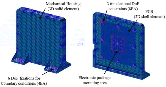
Figure 11.
Example of FEM of an electronics specimen.
Modal analysis was performed using the FE model based on the above modeling technique. The shapes of the 1st mode that most affected the housing and PCB for each case are shown in Figure 12, and the 1st to 3rd natural frequencies for each case are listed in Table 4. In Figure 12, the end of the housing structure is colored red, meaning that the largest displacement occurs in this area. All electronics cases exhibited global bending behavior in the first mode, and the elastic modes of the housing were mixed in the PCB. Furthermore, the solder joint of Case 1-1, where the electronic package was located at the edge of the PCB, failed in a shorter time than that of the electronic package of Case 1, owing to the influence of the modal shape of the package mounting area. Among the natural frequencies derived from the mode analysis, the first natural frequency was the most vulnerable because it generated the largest displacement in electronics. Therefore, the values in Equations (6) and (9) were applied to the first natural frequency of each case to evaluate the structural safety of the electronics using the Oh-Park methodology.
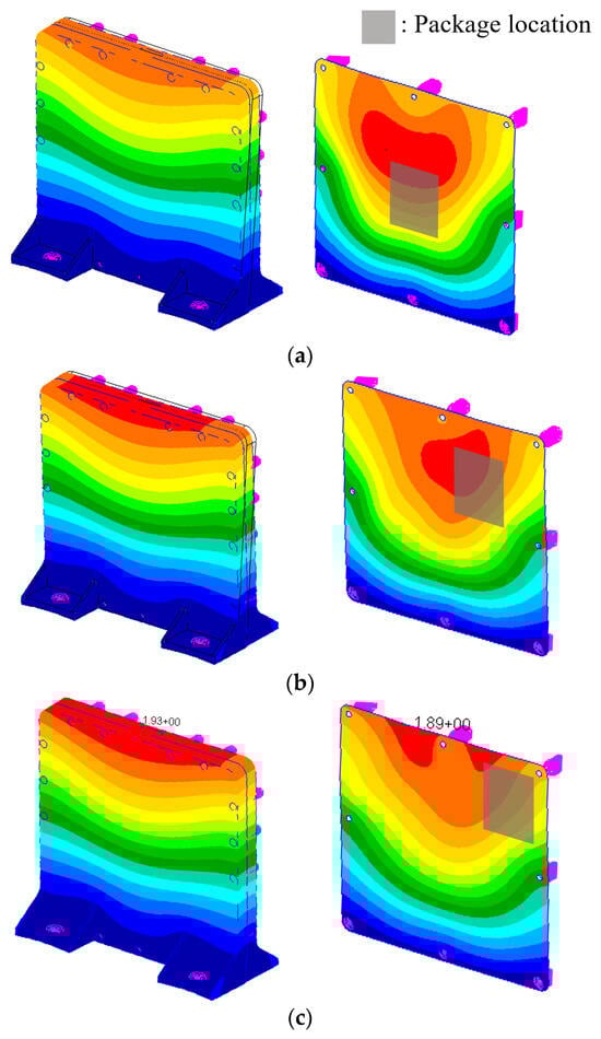
Figure 12.
First modal shapes of housing and PCB of specimens for each case ((a) Case 1, (b) Case 1-1, and (c) Case 1-2).
Table 4.
Analyzed values of for each case of electronics (1st–3rd modes).
A comparison of the predicted fatigue lives from testing and structural analysis was performed to demonstrate the validity of the Oh-Park methodology for electronics with a vertically mounted PCB, as shown in Figure 13.
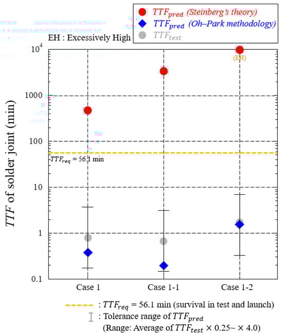
Figure 13.
Comparison of and estimated using the Steinberg and Oh-Park structural design methodologies.
The structural safety of the electronic package solder joints was evaluated using MoS calculations, and Equation (7) was applied to the calculations. For Steinberg’s theoretical analysis, the predicted fatigue life () was calculated using the power-law-based equation of the S-N curve, which is expressed as follows:
where denotes , which is the number of random vibration cycles in Steinberg’s conventional theory. , using the Oh-Park methodology, was calculated as follows:
The solder joints for the electronic package were composed of Sn-Pb37; thus, the value of b was 6.4.
As mentioned above, is used to calculate in the Oh-Park methodology, and Equation (6) is substituted with the first natural frequency obtained from the modal analysis. is calculated by averaging the RMS nodal strains of the cornermost QUAD4 element in the package that derives from random analysis. DF is derived from by applying Equations (8) and (9), and is shown in Table 5.
Table 5.
Estimations of for solder joints in test and launch processes.
The structural safety of the electronic package solder joints was evaluated by calculating the MoS for each factor. The estimated MoS values for the tested specimens are listed in Table 6, demonstrating that the results of the two structural design techniques are completely opposite. The MoS values calculated using Steinberg’s theory showed a positive margin, whereas those calculated using the Oh-Park methodology showed a negative margin. In the test, the specimens in all cases failed within a of 56.1 min, showing that the Oh-Park methodology with negative MoS was more representative of the test results than Steinberg’s theory.
Table 6.
Estimated MoS values for the tested specimens using the two methodologies.
For the based on Equations (10) and (11), Steinberg’s theory-based fatigue life was predicted to be approximately 600 to 140,000 times larger than that in the actual test, ranging from to s. In contrast, the Oh-Park methodology yielded more accurate predictions, with a difference of only 1.010–3.146 between the predicted and test lives. A difference of 3.146 times is a minor error in predicting the fatigue life of electronics because metallic materials, such as solder joints, are subject to large manufacturing or testing tolerances and correlation errors between FE modeling and testing.
Steinberg’s theory predicted that the lifetime of Case 1-1 would be longer than that of Case 1, which was the opposite of the test results. However, in the case of the Oh-Park methodology, structural safety was evaluated based on the dynamic characteristics of the electronics, as shown in Equation (6). Therefore, the failure sequences of Cases 1 and 1-1 were also reasonably predicted, owing to the mode shape. From this perspective, the effectiveness of the Oh-Park methodology-based structural safety evaluation was validated for electronics with vertically mounted PCBs. Furthermore, the Oh-Park methodology was proven to be more accurate than Steinberg’s theory.
5. Conclusions
This study applied the Oh-Park methodology to evaluate the structural safety of space-borne electronics based on the PCB strain. Furthermore, the effectiveness of a PCB mounted vertically in the housing was validated. Conventional structural design techniques cannot be applied to vertically mounted PCBs because the elastic modes are significantly affected by the bending behavior of the housing, which is fixed at only one end. Therefore, the main goal of this study was to apply the Oh-Park methodology, which was validated for horizontally mounted electronics and vertically mounted electronics. To this end, vibration tests were performed on electronic specimens that were intentionally designed to represent bending behavior. The results of the were compared with the MoS and values derived from the Oh-Park methodology and Steinberg’s conventional theory. The MoS calculated based on Steinberg’s theory showed positive values, unlike the test results where the solder joints failed before . However, the MoS values of all the specimens calculated using the Oh-Park methodology were negative, which reasonably represented the test results. In the case of TTF, Steinberg’s theory showed significant differences and did not predict the failure sequence in each test case. However, the estimation of the failure time using the Oh-Park methodology showed only minor differences that were acceptable, considering the tolerance levels of fatigue-life testing. Furthermore, the failure sequence of each case in the test could be accurately predicted by considering the dynamic characteristics of the structure to evaluate structural safety. The results prove that the Oh-Park methodology provides a faster and more accurate structural safety evaluation than that of Steinberg’s theory, even for a PCB with vertically mounted boundary conditions.
Author Contributions
Conceptualization, H.-U.O.; methodology, H.-U.O. and T.-Y.P.; validation, K.-W.K., T.-Y.P. and H.-U.O.; formal analysis, J.-H.P. and K.-W.K.; investigation, K.-W.K. and H.-U.O.; data curation, J.-H.P. and K.-W.K.; writing—original draft preparation, K.-W.K.; writing—review and editing, K.-W.K. and H.-U.O.; visualization, K.-W.K.; supervision, H.-U.O.; project administration, H.-U.O.; funding acquisition, H.-U.O. All authors have read and agreed to the published version of the manuscript.
Funding
This work was supported by a Korea Research Institute for Defense Technology Planning and Advancement (KRIT) grant funded by the Korean government Defense Acquisition Program Administration (DAPA). (KRIT-CT-22-040, Heterogeneous Satellite Constellation based ISR Research Center, 2022).
Data Availability Statement
The data presented in this study are available on request from the corresponding author.
Conflicts of Interest
Author Jae-Hyeon Park was employed by the company LIG Nex1, Co., Ltd. and authors Tae-Yong Park and Hyun-Ung Oh were employed by the company STEP Lab., Ltd. The remaining author declares that the research was conducted in the absence of any commercial or financial relationships that could be construed as a potential conflict of interest.
Abbreviations and Magnitudes
| PCB | Printed circuit board |
| FE | Finite element |
| MoS | Margin of safety |
| FoS | Factor of safety |
| BGA | Ball grid array |
| PBGA | Plastic ball grid array |
| CGA | Column grid array |
| SOP | Small-outline package |
| DIP | Dual in-line package |
| LCCC | Leaded ceramic chip carrier |
| Allowable displacement | |
| Maximum displacement | |
| ECSS | European Cooperation for Space Standardization |
| Critical value of PCB strain | |
| PCB in-plane principal strain | |
| Allowable PCB in-plane strain | |
| PCB RMS strain of x-direction | |
| PCB RMS strain of y-direction | |
| Strain rate of PCB | |
| DF | Design factor |
| Natural frequency | |
| TTF | Time to failure |
| Required time to failure | |
| Predicted time to failure | |
| Measured time to failure through test | |
| Sum of the fatigue time in the electronics level qualification test | |
| Sum of the fatigue time in the satellite system level acceptance test | |
| Sum of the fatigue time based on the fatigue experienced in the actual launch environment | |
| Safety factor for the time to failure | |
| Original fatigue cycles of Steinberg’s theory | |
| Required fatigue cycles of ground environment test and launch | |
| CoG | Center of gravity |
| S-N | Stress—number of cycles |
| g | Gram |
| RMS | Root mean square |
| Grms | Root mean square value of acceleration |
| DAQ | Data acquisition |
| PSD | Power spectral density |
| DoF | Degrees of freedom |
| RBE2 | Rigid body element 2 |
References
- Wijker, J.J. Spacecraft Structures; Springer Science & Business Media: Berlin/Heidelberg, Germany, 2008. [Google Scholar]
- Steinberg, D.S. Vibration Analysis for Electronic Equipment, 3rd ed.; John Wiley & Sons Inc.: New York, NY, USA, 2000. [Google Scholar]
- Kim, Y.K.; Hwang, D.S. PBGA packaging reliability assessments under random vibrations for space applications. Microelectron. Reliab. 2015, 55, 172–179. [Google Scholar] [CrossRef]
- Crandall, S.H.; Mark, W.D. Random Vibration in Mechanical Systems; Academic Press: Cambridge, MA, USA, 2014. [Google Scholar]
- Safarabadi, M.; Bazargan, S. Prediction of equivalent static loads act on a micro satellite via modal analysis. Eng. Solid Mech. 2015, 3, 75–84. [Google Scholar] [CrossRef]
- Depiver, J.A.; Mallik, S.; Amalu, E.H. Effect of Creep, Fatigue and Random Vibration on the Integrity of Solder Joints in BGA Package. Microelectron. Reliab. 2024, 157, 115415. [Google Scholar] [CrossRef]
- Jannoun, M.; Aoues, Y.; Pagnacco, E.; Pougnet, P.; El-Hami, A. Probabilistic fatigue damage estimation of embedded electronic solder joints under random vibration. Microelectron. Reliab. 2017, 78, 249–257. [Google Scholar] [CrossRef]
- Meyyappan, K.; Vujosevic, M.; Wu, Q.; Malatkar, P.; Hill, C.; Parrott, R. Knowledge Based Qualification Process to Evaluate Vibration Induced Failures in Electronic Components. In Proceedings of the ASME 2017 International Technical Conference and Exhibition on Packaging and Integration of Electronic and Photonic Microsystems Collocated with the ASME 2017 Conference on Information Storage and Processing Systems, San Francisco, CA, USA, 29 August–1 September 2017; p. V001T05A001. [Google Scholar] [CrossRef]
- An, T.; Qin, F.; Zhou, B.; Chen, P.; Dai, Y.; Li, H.; Tang, T. Vibration lifetime estimation of PBGA solder joints using Steinberg model. Microelectron. Reliab. 2019, 102, 113474. [Google Scholar] [CrossRef]
- Maniar, Y.; Konstantin, G.; Sharma, A.; Binkele, P.; Schmauder, S. Solder joint lifetime modeling under random vibrational load collectives. JOM 2020, 72, 898–905. [Google Scholar] [CrossRef]
- Saravanan, S.; Prabhu, S.; Muthukumar, R.; Raj, S.G.; Veerabagu, S.A. Fatigue failure of pb-free electronic packages under random vibration loads. Int. J. Comput. Methods Eng. Sci. Mech. 2018, 19, 61–68. [Google Scholar] [CrossRef]
- Oh, H.-U.; Jeon, S.-H.; Kwon, S.-C. Structural design and analysis of 1U standardized STEP Cube Lab for on-orbit verification of fundamental space technologies. Int. J. Mater. Mech. Manuf. 2014, 2, 239–244. [Google Scholar] [CrossRef]
- Grieu, M.; Massiot, G.; Maire, O.; Chaillot, A.; Munier, C.; Bienvenu, Y.; Renard, J. Durability modelling of a BGA component under random vibration. In Proceedings of the EuroSimE 2008—International Conference on Thermal, Mechanical and Multiphysics Simulation and Experiments in Microelectronics and Micro-Systems (EuroSimE 2008), Freiburg im Breisgau, Germany, 20–23 April 2008; pp. 1–8. [Google Scholar] [CrossRef]
- Jung, I.H.; Park, T.W.; Seo, J.H.; Han, S.W.; Kim, S.H. Structural vibration analysis of electronic equipment for satellite under launch environment. Key Eng. Mater. 2004, 270–273, 1440–1445. [Google Scholar] [CrossRef]
- Béda, M.G. A curvature-based interpretation of the Steinberg criterion for fatigue life of electronic components. Int. Symp. Microelectron. 2015, 2015, 707–712. [Google Scholar] [CrossRef]
- Kavitha, M.; Mahmoud, Z.H.; Kishore, K.H.; Petrov, A.M.; Lekomtsev, A.; Iliushin, P.; Zekiy, A.O.; Salmani, M. Application of Steinberg model for vibration lifetime evaluation of Sn-Ag-Cu-based solder joints in power semiconductors. IEEE Trans. Compon. Packag. Manuf. Technol. 2021, 11, 444–450. [Google Scholar] [CrossRef]
- Irvine, T. Extending Steinberg’s Fatigue Analysis of Electronics Equipment Methodology to a Full Relative Displacement vs. Cycles Curve; Revision C, Vibration Data 2013. Available online: https://www.vibrationdata.com/tutorials2/electronic_rd_n.pdf (accessed on 1 July 2024).
- Jeon, Y.-H.; Kim, H.-S.; Lim, I.-O.; Kim, Y.; Oh, H.-U. Mechanical reliability evaluation on solder joint of CCB for compact advanced satellite. J. Korean Soc. Aeronaut. Space Sci. 2017, 45, 498–507. [Google Scholar] [CrossRef]
- Park, T.-Y.; Oh, H.-U. New PCB strain-based structural design methodology for reliable and rapid evaluation of spaceborne electronics under random vibration. Int. J. Fatigue 2021, 146, 106147. [Google Scholar] [CrossRef]
- Park, T.-Y.; Park, J.H.; Oh, H.-U. Experimental evaluation of vibrational stability of SOPs in aerospace industry using PCB strain effectiveness of a PCB-strain-based design methodology. Aerospace 2023, 10, 516. [Google Scholar] [CrossRef]
- Park, T.-Y.; Oh, H.-U. Validation of the critical strain-based methodology for evaluating the mechanical safety of ball grid array solder joints in a launch random vibration environment. J. Electron. Packag. 2022, 144, 011006. [Google Scholar] [CrossRef]
- Park, J.-H.; Jeong, S.-K.; Oh, H.-U. Effectiveness of critical-strain-based methodology considering elastic mode vibration of mechanical housing of electronics. Aerospace 2023, 10, 974. [Google Scholar] [CrossRef]
- Kang, S.-J.; Park, S.-W.; Choi, H.-Y.; Ryu, G.-H.; Kim, J.-P.; Jung, S.-H.; Kim, S.-Y.; Lee, H.-I.; Oh, H.-U. Thermo-mechanical design and validation of spaceborne high-speed digital receiver unit for synthetic aperture radar application. Aerospace 2021, 8, 305. [Google Scholar] [CrossRef]
- ECSS-E-ST-32-10C Rev.1; Structural Factors of Safety for Spaceflight Hardware. European Cooperation for Space Standardization (ECSS): Noordwijk, The Netherlands, 2009.
- De Clerck, J.; Epp, D.S. Rotating Machinery, Hybrid Test Methods, Vibro-Acoustics & Laser Vibrometry, Volume 8: Proceedings of the 34th IMAC, A Conference and Exposition on Structural Dynamics 2016; Springer: Berlin/Heidelberg, Germany, 2016. [Google Scholar]
- Su, S.; Akkara, F.J.; Thaper, R.; Alkhazali, A.; Hamasha, M.; Hamasha, S. A state-of-the-art review of fatigue life prediction models for solder joint. J. Electron. Packag. 2019, 141, 040802. [Google Scholar] [CrossRef]
- Yunis, I.; Ludwiczak, D. On the use of 3dB qualification margin for structural parts on expendable launch vehicles. In Proceedings of the 48th AIAA/ASME/ASCE/AHS/ASC Structures, Structural Dynamics, and Materials Conference, Honolulu, HI, USA, 23–26 April 2007; pp. 1–9. [Google Scholar] [CrossRef][Green Version]
- ECSS-E-ST-32C; Structural General Requirements. European Cooperation for Space Standardization (ECSS): Noordwijk, The Netherlands, 2008.
- Chen, Y.S.; Wang, C.S.; Yang, Y.J. Combining vibration test with finite element analysis for the fatigue life estimation of PBGA components. Microelectron. Reliab. 2008, 48, 638–644. [Google Scholar] [CrossRef]
- IPC-9701A; Performance Test Methods and Qualification Requirements for Surface Mount Solder Attachments. Association Connecting Electronics Industries (IPC): Bannockburn, IL, USA, 2006.

Disclaimer/Publisher’s Note: The statements, opinions and data contained in all publications are solely those of the individual author(s) and contributor(s) and not of MDPI and/or the editor(s). MDPI and/or the editor(s) disclaim responsibility for any injury to people or property resulting from any ideas, methods, instructions or products referred to in the content. |
© 2024 by the authors. Licensee MDPI, Basel, Switzerland. This article is an open access article distributed under the terms and conditions of the Creative Commons Attribution (CC BY) license (https://creativecommons.org/licenses/by/4.0/).