Article

S-Parameter-Based Defect Localization for Ultrasonic Guided Wave SHM †

Murmann Mixed-Signal Group, Department of Electrical Engineering, Stanford University, 330 Jane Stanford Way, Stanford, CA 94305, USA
*
Author to whom correspondence should be addressed.
This paper is an extended version of our conference paper published at the 12th International Workshop on Structural Health Monitoring (IWSHM), Stanford, California, USA, 10–12 September 2019, which was selected for and invited to this special issue.
Aerospace 2020, 7(3), 33; https://doi.org/10.3390/aerospace7030033
Submission received: 28 February 2020 / Revised: 15 March 2020 / Accepted: 19 March 2020 / Published: 20 March 2020
(This article belongs to the Special Issue Selected Papers from IWSHM 2019)

Abstract

:
In this work, an approach for enabling miniaturized, low-voltage hardware for active structural health monitoring (SHM) based on ultrasonic guided waves is investigated. The proposed technique relies on S-parameter measurements instead of time-domain pulsing and thereby trades off longer measurement times with lower actuation voltages for improved compatibility with dense complementary metal-oxide-semiconductor (CMOS) chip integration. To demonstrate the feasibility of this method, we present results showing the successful localization of defects in aluminum and carbon-fiber-reinforced polymer (CFRP) test structures using S-parameter measurements. The S-parameter measurements were made on benchtop vector network analyzers that actuate the piezoelectric transducers at output voltage amplitudes as low as 1.264 Vpp.

1. Introduction

The increased use of high-performance composites and the need to lower maintenance costs while ensuring high standards of safety and reliability are prevailing trends in the aerospace industry. Together, these trends are fueling a shift from a schedule-based maintenance approach to a condition-based one [1,2]. In-situ structural health monitoring (SHM) systems are a key enabler of this condition-based maintenance paradigm because they can test the physical condition of structures in an automated, on-demand, and real-time fashion. Ultrasonic guided waves (UGWs) are a widely used modality in the implementation of SHM systems because they can travel long distances in thin-walled structures with minimal amplitude loss [1]. Furthermore, the transducers that excite UGWs can be easily incorporated into new and existing structures [3,4,5].
A key bottleneck in the deployment of in-situ UGW SHM systems is the use of data acquisition electronic systems that are bulky and unsuited for wide scale operation in the aircraft environment, which is highly sensitive to additional weight and volume. The electronic systems are large because they actuate the piezoelectric transducers that emit UGWs using sequences of short tone-burst pulses so as to minimize dispersion and maximize resolution [1]. To attain a receiver signal-to-noise ratio (SNR) that is good enough for the collected data to provide accurate defect detection and localization information, these tone-burst signals must have large amplitudes (~several tens to hundreds of volts) so as to have adequate energy to be distinguishable from noise. As a result, to withstand the large electric fields that are generated by these pulses, ultrasonic SHM systems are typically implemented using standard laboratory equipment [6,7,8] or bulky discrete electronic components [9,10].
An effective avenue towards the miniaturization of SHM electronics is the use of custom integrated circuits (ICs). In prior work in this area, our team presented a highly linear and energy-efficient four-channel piezo driver integrated circuit for UGW SHM [11]. However, this chip requires an external ±36 V power supply. This limits the chip’s scalability and necessitates the use of an expensive and area-inefficient 0.25 μm Bipolar-CMOS-DMOS fabrication process. In more recent work, Tang et al. demonstrated a compact single-channel 12.7 Vpp transceiver for SHM [12,13]. However, this design still requires an external high-voltage power amplifier for typical use cases.
This work is inspired by the 2014 work of Huang and Bednorz, which introduced the use of scattering parameters (S-parameters) for UGW SHM [14]. Using measurements made on a benchtop vector network analyzer (VNA), they showed that ultrasound pitch-catch, pulse-echo, and electro-mechanical impedance signals can be recovered from the S-parameters of a structure under test. These signals have a higher SNR and larger dynamic range than the corresponding time-domain signals measured on an oscilloscope, and thus require significantly smaller actuation voltages. In follow-on work, it was also established that S-parameter measurements allow for convenient time-frequency analysis for SHM [15,16].
Our recent conference publication demonstrated, for the first time, the use of S-parameter measurements for the localization of defects in an aluminum test structure [17]. In this paper, we extend this work to also show S-parameter-based defect localization in a carbon-fiber-reinforced polymer (CFRP) test structure and then leverage the insights we gain to propose a frequency-domain-based on-chip system for ultrasonic SHM. The rest of this paper is organized as follows. Section 2 provides some background on S-parameters and their use in ultrasonic guided-wave SHM. Focus is placed on explaining how VNAs can exploit longer measurement times to make high SNR measurements at low output signal amplitudes that are compatible with CMOS IC fabrication technology. In Section 3, the experimental setup that was used to validate the use of S-parameter measurements in the localization of defects in aluminum and CFRP test structures is described. The results of these experiments are presented in Section 4. Finally, Section 5 discusses the future direction of this work and concludes the paper.

2. Background

S-parameters are widely used in electrical engineering to describe the behavior of linear, multi-port electrical networks in response to stimulation by electrical signals. Figure 1 shows the S-parameter representation of a two-port electrical network. Four S-parameters represent the reflection coefficients at Ports 1 and 2 (S11 and S22) and the transmission coefficients (gains) from Port 1 to Port 2 (S21) and Port 2 to Port 1 (S12). In this diagram, a1 and a2 are the input signals at Ports 1 and 2, respectively. Similarly, b1 and b2 are the reflected signals at those ports. Since the inputs and outputs of an ultrasonic SHM system are electrical signals, the paths between transducers through the structure can be characterized using S-parameters if the Lamb waves travelling on them exhibit properties that are linear and time-invariant.
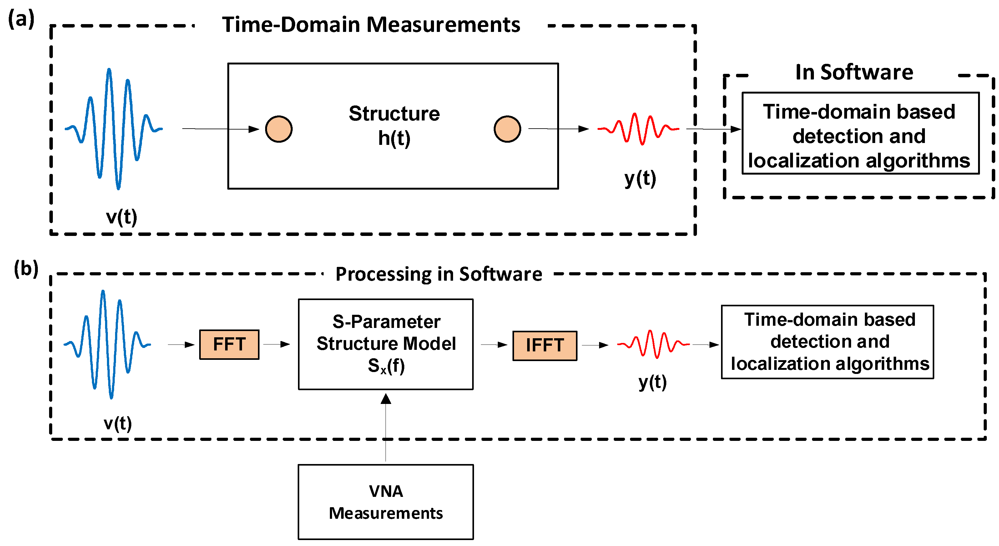
From signal processing, we know that a signal can be represented both in the time-domain and the frequency-domain. Even though they emphasize different properties of the signal, these representations are equivalent, and each contains all the information that we need to fully characterize the signal. Furthermore, a signal can be translated between these two equivalent representations without information loss by appropriately applying the Fourier Transform and its inverse to the signal. Figure 2 shows a comparison between the traditional time-domain approach to ultrasonic SHM and the S-parameter approach. As shown, Fourier Transform methods enable the use of S-parameters for SHM while allowing for the maintained use of well-established [18,19,20] and emerging [21,22,23] time-domain-based algorithms for detecting and localizing defects.
The voltage amplitudes applied to the lead zirconate titanate (PZT) piezoelectric transducers in the measurement of S-parameters for SHM in prior work [14] are of particular interest to our efforts to implement custom integrated circuits for ultrasonic SHM. In that work, S-parameter measurements were made with a VNA that actuated the piezoelectric transducers with sinusoidal waveforms at an output power of +10 dBm. This translates to a peak-to-peak voltage of just two volts across a 50 Ω load and four volts across a high impedance load, such as a PZT transducer. In both cases, this is a dramatic reduction when compared to the several tens of volts that are used in typical time-domain ultrasonic SHM systems. The time-domain waveforms that were subsequently generated using these S-parameters were compared to oscilloscope measurements and were in good agreement with them while displaying higher signal-to-noise ratio and larger dynamic range. To better understand how the VNA measurements achieve better SNR and dynamic range while actuating the PZT transducers at dramatically lower voltages, the architecture and operation of a VNA is briefly described in the sub-section below.

2.1. Vector Network Analyzers

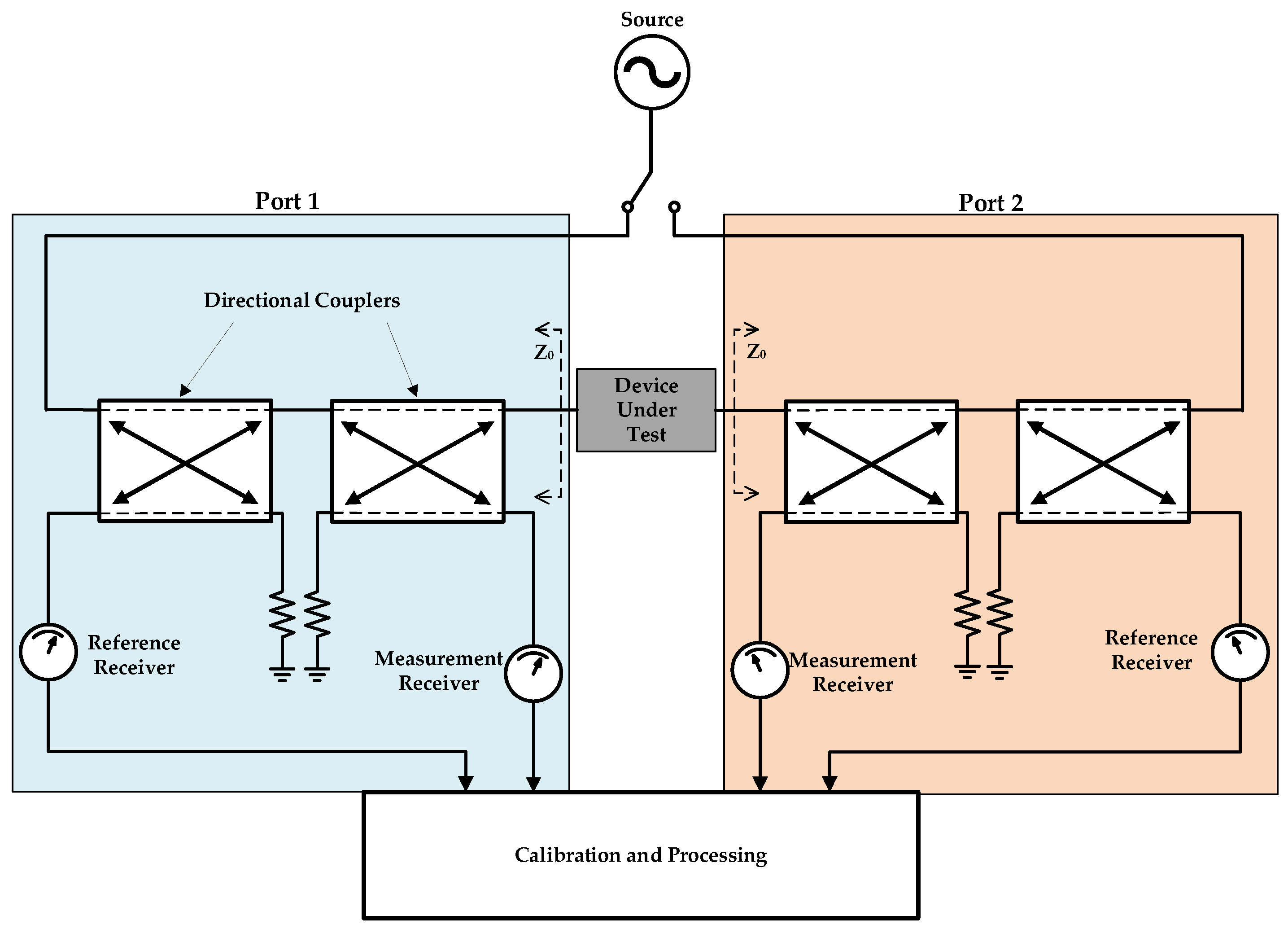
A VNA measures the S-parameters of a device under test (DUT) by directly measuring the component signals shown in Figure 1 in a vector (both magnitude and phase) fashion. Once these measurements have been taken, they are subsequently used to calculate the S-parameters according to the expressions shown in Figure 1. The sub-systems required to make these measurements in a typical VNA system are a signal source, signal separation hardware, measurement receivers and a processing backend. The architecture of a two-port VNA is shown in Figure 3 and the component sub-systems are described in the following sub-sections.

2.1.1. Signal Source

The source provides the stimulus signal that is injected into the DUT to initiate the characterization. The signal is sinusoidal, and it can excite the DUT at a single frequency or more commonly across a sequence of predetermined frequencies in the bandwidth of interest. Since VNA ports are usually stimulated sequentially, sources often include a transfer switch such as the one shown in Figure 3 to enable the use of the same source at both ports and, more generally, each port in an N-port network analyzer.

2.1.2. Signal Separation Hardware

At each port, the reference and reflected signals travel on the same transmission line but they need to be measured independently to determine the S-parameters. A characteristic of the signals that can be used to separate them is their direction of travel along the transmission line. Directional elements such as directional couplers, directional bridges, circulators, and Wilkinson dividers can be used for this purpose. In VNA systems, directional couplers are more commonly used than the other kinds of directional elements.
Figure 4 shows the structure of a generic four port directional coupler. Ports 1 and 2 are directly connected and form the main line of the coupler and the signal travels between them with minimal loss. Ports 3 and 4 are also directly connected to form the auxiliary line of the coupler. The signal also travels along this line with minimal loss. An electromagnetic or electrical coupling mechanism transfers a well-defined fraction of the signal power from the main line to the auxiliary line. The signal transferred to the auxiliary line can then be used in another circuit, such as a measurement circuit, with minimal disruption to the signal on the main line. To give the coupler its directional properties, this coupling mechanism works in such a way that a signal traveling in one direction (for example, Port 1 to Port 2) couples much more strongly to the auxiliary line than a signal travelling in the opposite direction (Port 2 to Port 1). The key performance characteristic of a directional coupler is its directivity. Directivity is a measure of how much more strongly a signal travelling in the desired direction couples to the auxiliary line than the unwanted signal travelling in the reverse direction. Directivity is one of the major factors affecting the accuracy of a VNA’s measurements [24,25,26].

2.1.3. Measurement Receivers

These receivers measure the magnitude and phase of the reference and reflection signals after the signal separation stage. A typical measurement receiver consists of an analog part and a digital part. The analog portion of the receiver is most widely implemented as a heterodyne receiver that mixes the input signal with a local oscillator (LO) signal to yield a signal at a much lower intermediate frequency (IF). Figure 5 shows such a heterodyne receiver architecture. This receiver architecture is favored because subsequent filtering at the IF frequency results in a smaller receiver bandwidth, and this has the advantage of minimizing the integrated broadband noise which in turn improves receiver sensitivity and dynamic range. The IF filter also doubles up as an anti-aliasing filter for the analog-to-digital converter (ADC), and sampling and conversion at the lower IF also relaxes the design requirements of the ADC, especially in microwave applications. Once the signal is converted to digital form, the digital signal processing (DSP) portion of the receiver does further processing to measure the magnitude and phase of the signal as required.

2.1.4. Processing Backend

Once the magnitude and phase measurements of the signals are taken, they are further processed to yield the S-parameters and to format them into representations that are easy to use and interpret for a wide variety of applications. Examples of these are magnitude-phase plots, real-imaginary plots, Smith charts, polar plots, linear sweeps, logarithmic sweeps and other such formats. In addition to this, the processing backend also performs error correcting functions such as averaging, calibration, embedding/de-embedding, power correction, and other such functions.

2.2. Attaining Higher SNR

The sensitivity of a measurement system is the minimum signal level that it can receive with acceptable quality. Sensitivity is determined by the thermal noise floor, the measurement bandwidth, the additional noise introduced by the system, and the minimum SNR required by the system. At room temperature (298 K), this relationship is captured in Equation (1), as shown below [27]:
Pmin = −174 dBm + NF + 10log(B) + SNRmin,
In this equation, Pmin is the minimum acceptable signal power in dBm, −174 dBm is the thermal noise floor (a function of the Boltzmann constant and temperature), NF is the system’s noise figure in decibels (dB), B is the measurement bandwidth in hertz (Hz) and SNRmin is the system’s minimum SNR requirement in dB. Taken together, the first three terms on the right define the system’s noise floor.
Once the minimum SNR requirement is fixed, Equation (1) says that there are two ways in which the minimum acceptable signal level can be lowered. The first method is to reduce the system’s noise figure by improving the system’s noise performance. This comes at the cost of increased power consumption, a larger area, increased design effort, and several other factors. The second way to improve sensitivity is to reduce the bandwidth over which the measurement is taken. As illustrated in Figure 6, reducing the bandwidth reduces the broadband noise that is captured alongside the signal that we are interested in measuring and this reduction in the captured noise results in higher SNR. Lowering the measurement bandwidth comes at the cost of increasing the time over which the measurement is taken. The two quantities are inversely related through the time-frequency uncertainty principle.
VNAs exploit the second method to a achieve high sensitivity. The user can vary the measurement bandwidth by adjusting the intermediate frequency filter bandwidth (IFBW). Taking a case where the IFBW is reduced by a factor of N, Equations (2) to (4) below show the expected improvement in sensitivity.
Pmin,new = −174 dBm + NF + 10log(Bnew) + SNRmin,
Pmin,new = −174 dBm + NF + 10log(B0/N) + SNRmin,
Pmin,new = −174 dBm + NF + 10log(B0) + SNRmin − 10log(N),
It is clear that to satisfy the same SNR requirement, Pmin,new can be up to 10log(N) times smaller than the power of the minimum acceptable signal at the initial measurement bandwidth, B0. If the signal is sinusoidal, this translates to a N smaller amplitude and this benefit comes at the cost of an N-fold increase in the measurement time. It is worth noting that the VNA measurements are made in the frequency domain, hence this sensitivity improvement manifests itself as a better measurement of the S-parameters. However, through Parseval’s theorem, the total noise energy of a signal in the frequency domain is equal to the total noise energy of that same signal in the time domain. Hence, the higher quality spectrum measurements at a smaller IFBW translate to higher quality time-domain waveforms when the inverse Fourier transform is applied to the spectrum.
The principle described above is what was exploited in prior work to make low-voltage VNA-based SHM measurements that have much better SNR performance than time-domain measurements [14]. In that work, the following VNA parameters were identified as the key ones affecting the duration and quality of the generated time-domain signals: the VNA frequency step, VNA starting frequency, VNA ending frequency, and the VNA intermediate frequency filter bandwidth (IFBW).
Before designing and implementing SHM hardware based on S-parameter measurements, it is important to demonstrate the utility of these measurements in detecting and localizing defects. In the next section, we describe and report the results of defect localization experiments that we conducted in widely used aerospace materials.

3. Materials and Methods

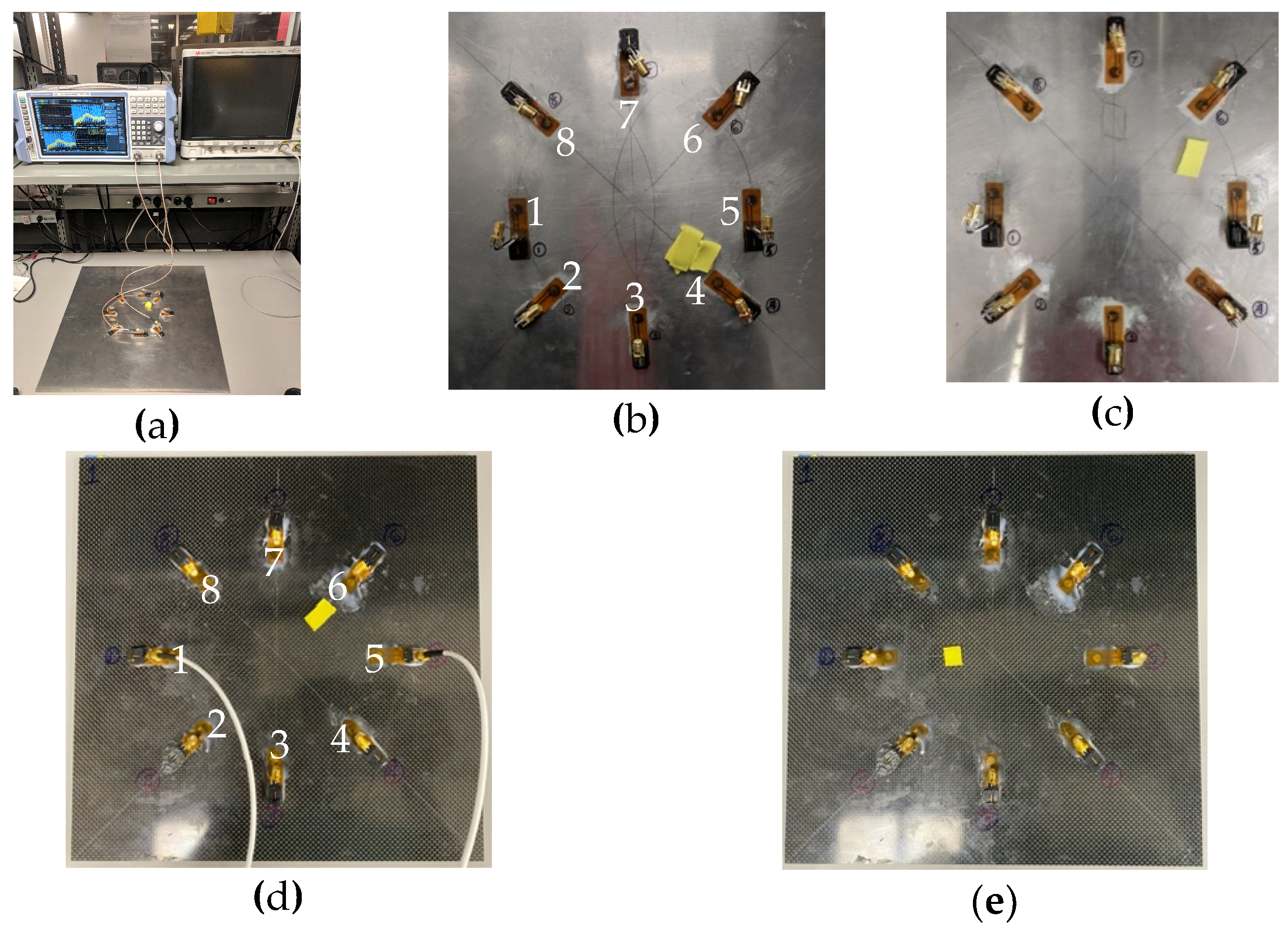
Experiments to validate the S-Parameter damage localization method were carried out in aluminum and carbon-fiber-reinforced polymer (CFRP) plates. These test structures are shown in Figure 7 and we provide details on how they were prepared and how the measurements were taken in Appendix A. After taking the measurements, the S-parameters for each transducer-to-transducer path are extended to have a starting frequency of 0 Hz by zero-padding. They are then combined with a digitally generated input tone-burst waveform, v(t), to generate time-domain signals for defect localization using the procedure described below and illustrated in Figure 8. First, the Discrete Fourier Transform (DFT), V(f), of the input tone-burst was taken. For each transducer-to-transducer path, the frequency spectrum of the pitch-catch output signal, Y(f), was obtained by multiplying V(f) and the path’s S21(f). Finally, the time-domain pitch-catch signal, y(t), was generated by taking the Inverse Discrete Fourier Transform (IDFT) of Y(f). These time-domain pitch-catch signals then served as inputs to the widely used reconstruction algorithm for probabilistic inspection of defects (RAPID), which we used for damage localization [18].

4. Results

The results of the S-parameter measurements taken in both aluminum and composite materials are presented in this section. In both materials, the measured S21 spectra for select transducer-to-transducer paths are presented followed by the time-domain waveforms generated from the spectra. After this, the defect localization maps generated from the time domain waveforms at a number of different frequencies are shown.

4.1. Results of the Aluminum Test Structure

Figure 9 shows the S21 parameter plots for the paths between PZT 1 and PZT 8 as well as PZT 4 and PZT 8 (baseline and defective cases with the defect at Location 1). These paths were chosen to compare the case of not passing through the defect versus passing directly through the defect. As expected, there are more pronounced differences in the baseline and defect spectra for the latter case.
In particular, some attenuation is observed in the defect state S21 magnitude spectrum for the PZT 4 to PZT 8 path across all frequencies, but especially at frequencies above 700 kHz. This attenuation is likely due to the absorption of some of the Lamb waves’ energy by the sealant material that acts as a defect in our experiments. Furthermore, there is greater deviation across a wider range of frequencies in the phase spectra of the PZT 4 to PZT 8 path. We suspect that this greater deviation can be attributed to a greater degree of interaction between the defect and the Lamb waves travelling on this path as compared to the more distant PZT 1 to PZT 8 path. Finally, since the phase spectra are approximately linear and the phase spectrum under the defect condition for the PZT 4 to PZT 8 path lies under the baseline phase spectrum, we expect to see slightly more delay in the time-domain waveforms for the defect case and this is confirmed in the waveforms in Figure 10.
The time-domain waveforms generated from S21 for different paths, including the PZT 1 to PZT 8 and PZT 4 to PZT 8 paths, are shown in Figure 10. The digitally generated input tone-burst has an amplitude of 20 V and is centered at 300 kHz. The defect was at Location 1. Each plot shows the first 100 μs of the 4 ms record length. In addition to the output voltages in the baseline and defective states, each plot shows the scatter signal, which is obtained by baseline subtraction. The amplitudes of the output waveforms range from 11.2 mV to 29.6 mV, corresponding to attenuations of ~100 times (40 dB) relative to the input.
For Paths 1-to-8 and 3-to-8, which do not pass through the defect, the waveforms for the baseline and defective conditions are almost identical and they yield scatter signals with maximum amplitudes of about 0.5 mV. For Paths 3-to-5 and 4-to-8, the outputs for the defective case show significant attenuation, as predicted by the S21 amplitude spectra. As a result, with maximum amplitudes of 2.5 mV and 4.7 mV, respectively, the scatter signals are almost an order of magnitude larger than those of Paths 1-to-8 and 3-to-8.
Figure 11 shows damage localization results for the two aluminum defects for a generated input tone-burst signal centered at 300 kHz. As the images show, there is good agreement between the physical defect locations and sizes and the damage localization maps generated using the RAPID algorithm. In generating these images, the value of β, the parameter that controls the size of the effective elliptical distribution area, was set to 1.05 in line with the guidance on preserving a good resolution while minimizing artifacts that was given in the work that pioneered the method [18]. Once they have been measured, the S-parameters enable easier comparison of detection and localization results at different frequencies than the traditional time-domain approach. Waveforms at new frequencies can be generated from the recorded S-parameter measurements and processed for detection and localization purposes in a matter of seconds rather than reconfiguring a time-domain-based measurement system to take a new set of measurements at each new frequency. Consequently, this enables the efficient identification of optimal test frequencies for a wide variety of defects across different materials. Figure 12 shows the defect localization results for the two aluminum defect locations at 150 kHz, 300 kHz, and 500 kHz. As the images show, there is some variation with frequency in the localization results, and, in this case, the results at 300 kHz exhibit the best correspondence to the damage locations.

4.2. Results of the CFRP Test Structure

The results of the CFRP coupon largely follow the same trends as those observed in aluminum. Figure 13 shows the S21 spectra of two equidistant paths emanating from PZT 3 with the defect at Location 1. Path 3-to-8 is far from the defect and Path 3-to-6 passes through the defect. In these spectra, the patterns in magnitude attenuation and phase deviation due to defect introduction are similar to those seen in the aluminum spectra.
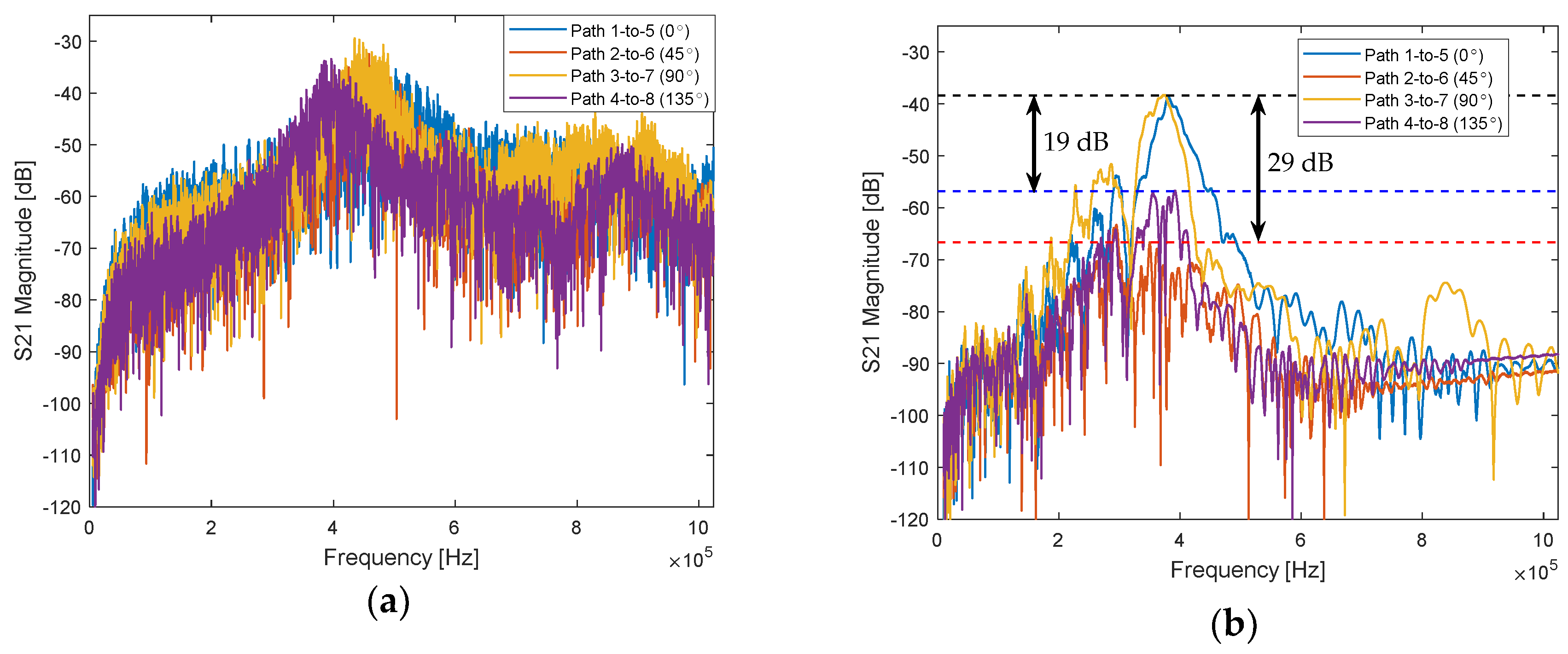
A notable difference in the S21 spectra of the CFRP relative to those measured in aluminum is the effect of orientation on the S21 magnitude. Figure 14 shows the S-parameter spectra of equidistant paths with different angles of orientation. The angles of orientation are measured in a counterclockwise fashion relative to the positive x-axis of an x–y-axis whose origin is at the center of each test panel. As the figure shows, the angle of orientation does not introduce any discernable difference in the aluminum S21 magnitude spectra. In CFRP, however, a distinct difference is observed between paths that run at the 0° and 90° orientations that align with the directions of the fiber weave of the composite plate and the 45° and 135° paths that run diagonal to the weave. At the peaks, the paths that run along the directions of the weave have peak S21 magnitudes that are comparable to the ones measured in aluminum (~ −40 dB) and are at least 19 dB and up to 29 dB greater than those of the diagonal paths in the same material. This difference is testament to the anisotropic nature of the CFRP’s properties. These plots also show that there is a wide dynamic range of up to 90 dB in S21 magnitude in both materials across the tested frequency range. As discussed earlier, a VNA is well suited to make measurements across such a wide dynamic range.
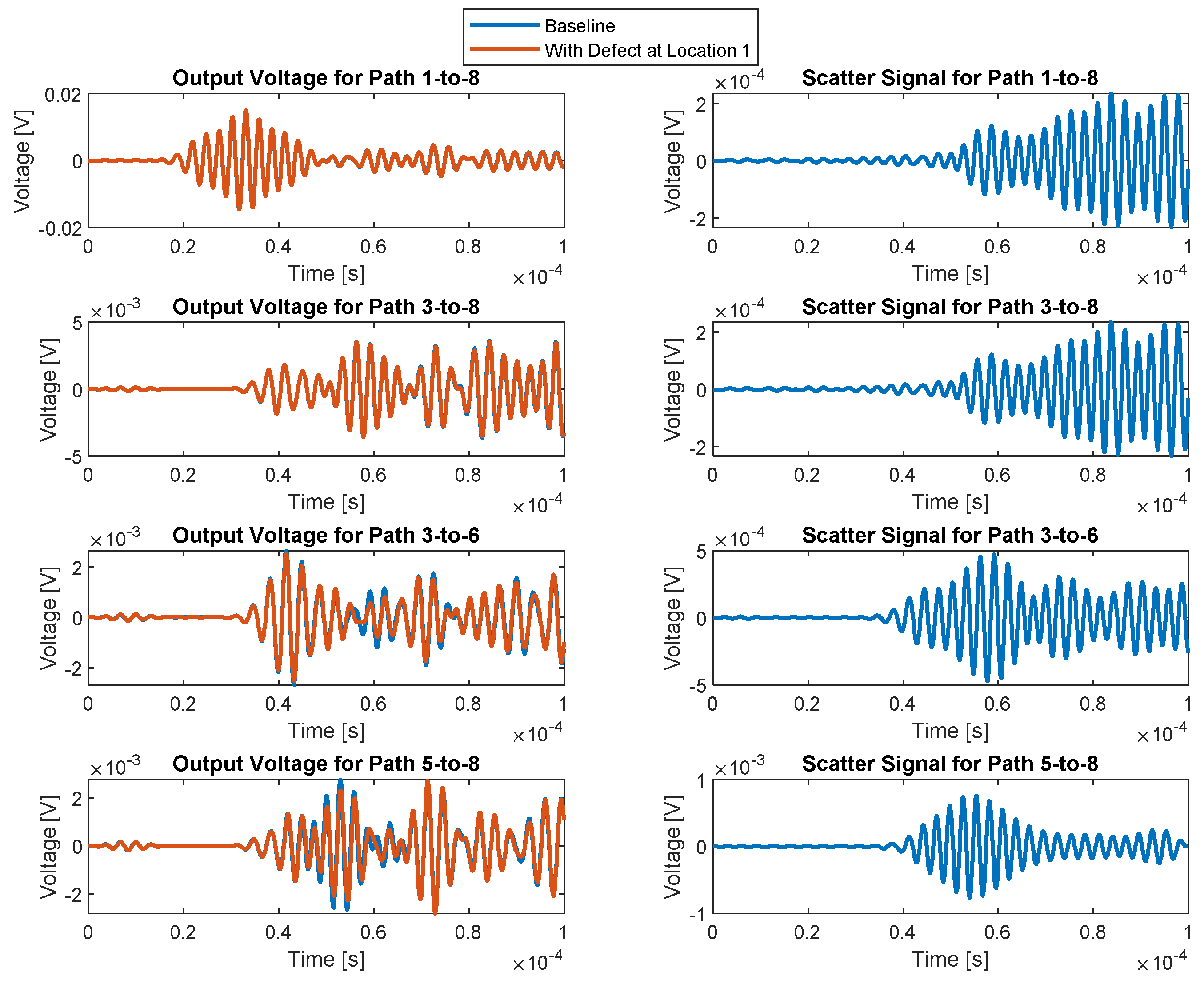
A few time-domain waveforms that are generated from S21 measurements for the first defect location in CFRP are shown in Figure 15. As was the case in aluminum, Path 1-to-8 and Path 3-to-8, which are far from the defect, are unaffected and exhibit very small scatter signals, whereas Path 3-to-6 and Path 5-to-8 exhibit the attenuation, slight delay, and larger scatter signals that are characteristic of the presence of the surface defect that was introduced.
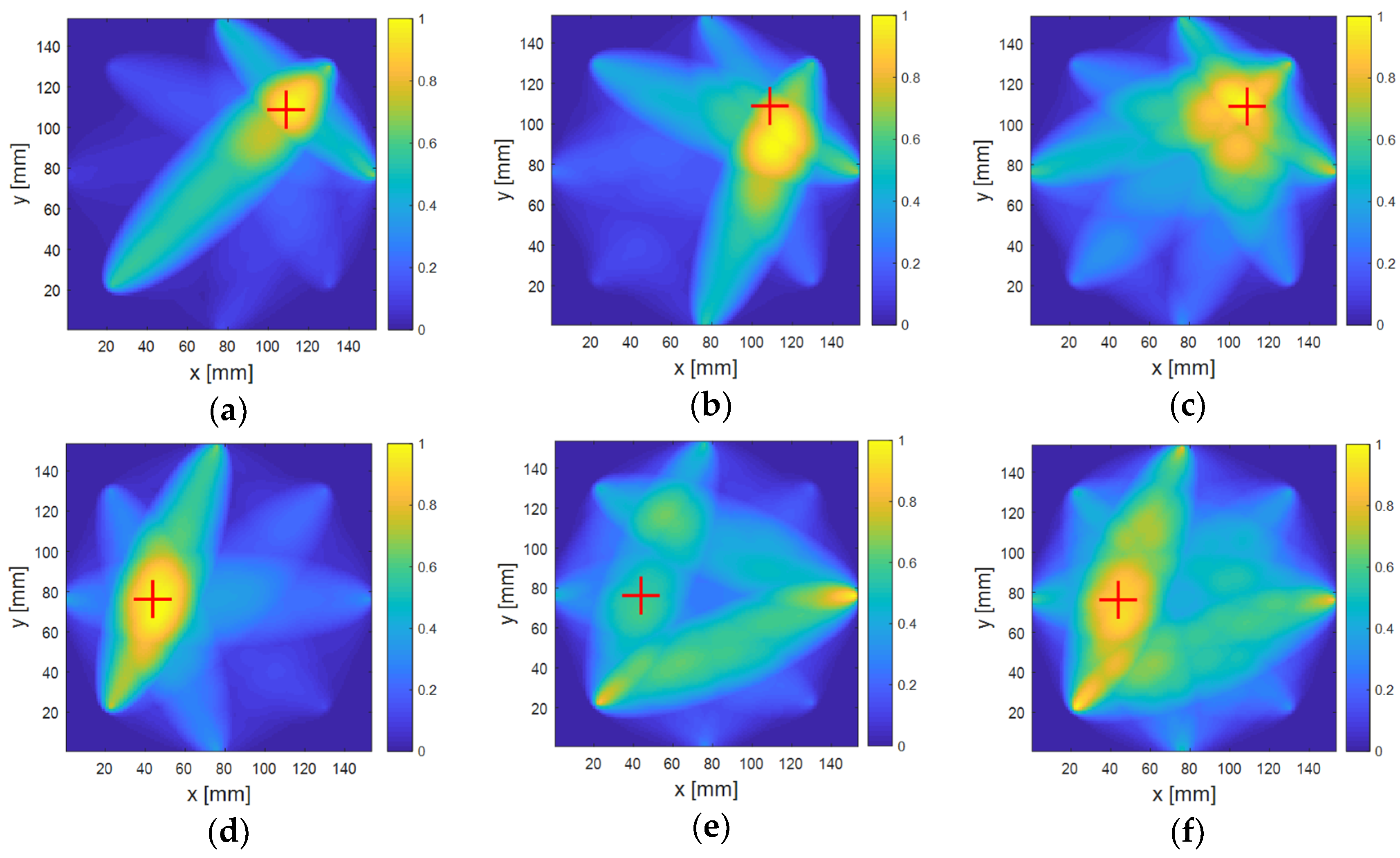
The damage localization results of the two defects introduced on the CFRP panel are shown in Figure 16. For Location 1, localization was successful at all tested frequencies with some variation in the size of the defect hot spot. For Location 2, the predicted defect location is clear and corresponds to the true location for tests at 150 and 500 kHz, with unclear results at 300 kHz. This shows the difference that the test frequency can make in the quality of the localization results and the value of the S-parameter approach in efficiently generating waveforms and defect maps at several frequencies from a single set of measurements.

5. Discussion and Conclusions

The results presented in this work show the successful use of S-parameter measurements and Fourier Transform techniques to perform ultrasonic guided wave RAPID defect localization in materials that are widely used in the aerospace industry. The advantage of this approach is that actuation voltages that are up to 100 times smaller than those used in time-domain-based SHM systems can be applied to the PZT transducers while still yielding signals with good SNR and a wide dynamic range. However, the S-parameters were measured using benchtop VNAs, which are very expensive and share the same limitations with time-domain ultrasonic SHM systems in size and portability. To address this drawback, the compatibility of the low-amplitude stimulation signals used in this work with commercial CMOS integrated circuit fabrication technology can be exploited to build a measurement platform of greatly reduced size and cost. Indeed, such an approach has been taken to realize VNA-on-a-chip systems that make S-parameter measurements in microwave-based biomedical sensors [28,29].
The next steps in our work are specifying and implementing such a system for SHM applications. Even though the measurements that were made in this work to exploit time-frequency equivalency are S-parameters, it is worth exploring if other frequency domain transfer functions can achieve the same quality of results at such low voltages. One such transfer function which would be easier to measure than the S-parameters is the voltage gain (both magnitude and phase) from the input piezoelectric transducer to the output piezoelectric transducer. Another area that requires further investigation is the sensitivity of this method to physical and environmental variables, such as adhesive type and quantity, inter-sensor distance, and temperature variation. The results of these explorations will in turn influence the requirements and construction of the integrated-circuit frequency-domain-based SHM system that we envision.

Author Contributions

Conceptualization, G.N. and B.M.; Investigation, G.N.; Methodology, G.N.; Software, G.N.; Supervision, B.M.; Validation, G.N.; Visualization, G.N.; Writing—original draft, G.N.; Writing—review & editing, B.M. All authors have read and agreed to the published version of the manuscript.

Funding

The proposed work was funded in part by Acellent Technologies through funding from Air Force STTR Contract #FA9550-18-C-0009.

Acknowledgments

The authors acknowledge the support of Acellent personnel and the contract monitor Byung L. Lee from the Air Force Office of Scientific Research (AFOSR) in this effort.

Conflicts of Interest

The authors declare no conflict of interest. The funders had no role in the design of the study; in the collection, analyses, or interpretation of data; in the writing of the manuscript, or in the decision to publish the results.

Appendix A. Experimental Details

The aluminum plate is made of the 6061 alloy and measures 457.2 mm × 457.2 mm × 3 mm. The ultra-strength lightweight CFRP composite plate used was sourced from McMaster-Carr (Elmhurst, IL, USA), Product Number–8181K16, and has dimensions of 304.8 mm × 304.8 mm × 3.2 mm. On each of the plates, eight Acellent SMLSSOP4NR 0.25-inch PZT transducers were mounted using LOCTITE EA E-20HP epoxy. On both test coupons, the transducers are arranged in 152.4 mm diameter circles with the one in aluminum centered at the coordinates (228.6 mm, 228.6 mm) and the one in CFRP centered at (152.4 mm, 152.4 mm) with the origin being in the bottom left corner of the plate in each case. Damage detection and localization was done within these circles. SMA connectors were mounted on all the PZT transducers to provide a standard interface for the measurement of the S-parameters.
In each coupon, there are 28 unique transducer-to-transducer paths between the 8 transducers and baseline S-Parameters were measured for each of these paths. After taking baseline measurements, artificial defects in the form of patches of AT-200Y sealant by General Sealants (City of Industry, CA, USA) were introduced to the structure. In aluminum, the first patch was centered at coordinates (265 mm, 192.2mm) and measured 25 mm by 18 mm. The second patch in aluminum was centered at coordinates (277.6 mm, 252.1 mm) and measured 23 mm × 13 mm. In CFRP, the first defect was centered at (185 mm, 185 mm) and measured 24 mm × 12 mm, the second was centered at (120 mm, 152.4 mm) and measures 12 mm × 12 mm. After the introduction of each defect, a new set of S-parameter measurements was taken in the respective structure. Figure 7 shows the measurement setup and the defect locations in both structures.
Measurements in aluminum were made using a two-port Rohde & Schwarz (Munich, Germany) ZNL3 VNA. The VNA output power was set to 0 dBm and this translates to an output voltage of 1.264 Vpp when the source is interfaced to a PZT transducer. The stimulus signal was swept from 5 kHz to 1.024 MHz. This frequency range was swept in 250 Hz steps to enable an alias-free range of up to 4 ms in the generated time-domain signals. Finally, a 100 Hz IFBW was chosen to achieve good SNR and high dynamic range. Under these conditions, it took 85.6 s to measure the S-parameters of each transducer-to-transducer path.
The measurements in the CFRP coupon were taken using a Rohde & Schwarz ZNB4 VNA. A higher output power of 10 dBm (4 Vpp into a PZT load) was used to compensate for the higher levels of signal attenuation in some directions due to the anisotropicity of the CFRP material. The frequency range was adjusted to 10 kHz to 1.024 MHz due to the higher lower frequency limit of the ZNB4. The 250 Hz frequency steps and 100 Hz IFBW were maintained, and the measurement time reduced slightly to 85.5 s per transducer-to-transducer path.

References

  1. Giurgiutiu, V. Structural Health Monitoring with Piezoelectric Wafer Active Sensors, 2nd ed.; Elsevier: Amsterdam, The Netherlands, 2014. [Google Scholar]
  2. Giurgiutiu, V. Structural Health Monitoring of Aerospace Composites, 1st ed.; Academic Press: London, UK, 2016. [Google Scholar]
  3. Lin, M.; Chang, F. The manufacture of composite structures with a built-in network of piezoceramics. Compos. Sci. Technol. 2002, 62, 919–939. [Google Scholar] [CrossRef]
  4. Wang, Y.; Qiu, L.; Luo, Y.; Ding, R. A stretchable and large-scale guided wave sensor network for aircraft smart skin of structural health monitoring. Struct. Health Monit. 2019. [Google Scholar] [CrossRef]
  5. Shen, Z.; Chen, S.; Zhang, L.; Yao, K.; Tan, C. Direct-Write Piezoelectric Ultrasonic Transducers for Non-Destructive Testing of Metal Plates. IEEE Sens. J. 2017, 17, 3354–3361. [Google Scholar] [CrossRef]
  6. Philibert, M.; Soutis, C.; Gresil, M.; Yao, K. Damage Detection in a Composite T-Joint Using Guided Lamb Waves. Aerospace 2018, 5, 40. [Google Scholar] [CrossRef] [Green Version]
  7. Wang, S.; Wu, W.; Shen, Y.; Liu, Y.; Jiang, S. Influence of the PZT Sensor Array Configuration on Lamb Wave Tomography Imaging with the RAPID Algorithm for Hole and Crack Detection. Sensors 2020, 20, 860. [Google Scholar] [CrossRef] [PubMed] [Green Version]
  8. Zeng, L.; Huang, L.; Lin, J. Damage imaging of composite structures using multipath scattering Lamb waves. Compos. Struct. 2019, 216, 331–339. [Google Scholar] [CrossRef]
  9. Capineri, L.; Bulletti, A.; Calzolai, M.; Giannelli, P.; Francesconi, D. Arrays of Conformable Ultrasonic Lamb Wave Transducers for Structural Health Monitoring with Real-time Electronics. Procedia Eng. 2014, 87, 1266–1269. [Google Scholar] [CrossRef] [Green Version]
  10. Zhang, D.; Yu, P.; Beard, S.; Qing, P.; Kumar, A.; Chang, F. A new SMART sensing system for aerospace structures. In Unmanned Systems Technology IX, 656107; Proc. SPIE 6561: Orlando, FL, USA, 2007. [Google Scholar]
  11. Guo, Y.; Aquino, C.; Zhang, D.; Murmann, B. A Four-Channel, ±36 V, 780 kHz Piezo Driver Chip for Structural Health Monitoring. In Proceedings of the 39th European Solid-State Circuits Conference, Bucharest, Romania, 16–20 September 2013; pp. 85–88. [Google Scholar]
  12. Tang, X.; Zhao, H.; Mandal, S. A programmable CMOS transceiver for structural health monitoring. In Proceedings of the 2018 IEEE Custom Integrated Circuits Conference (CICC), San Diego, CA, USA, 8–11 April 2018. [Google Scholar]
  13. Tang, X.; Harley, J.; Bi, K.; Ozdemir, T.; Pawloski, M.; Mandal, S. Sparse Sensor Networks for Active Structural Health Monitoring Using Highly Integrated CMOS Transceivers. In SPIE Smart Structures and Materials + Nondestructive Evaluation and Health Monitoring; SPIE 10598: Denver, CO, USA, 2018. [Google Scholar]
  14. Huang, H.; Bednorz, T. Introducing S-parameters for ultrasound-based structural health monitoring. IEEE Trans. Ultrason. Ferroelectr. Freq. Control. 2014, 61, 1856–1863. [Google Scholar] [CrossRef] [PubMed]
  15. Zahedi, F.; Huang, H. Time-frequency analysis of electro-mechanical impedance (EMI) signature for physics-based damage detections using piezoelectric wafer active sensor (PWAS). Smart Mater. Struct. 2017, 26, 055010. [Google Scholar] [CrossRef]
  16. Islam, M.; Huang, H. Detecting severity of delamination in a lap joint using S-parameters. Smart Mater. Struct. 2018, 27, 035006. [Google Scholar] [CrossRef]
  17. Nyikayaramba, G.; Murmann, B. Towards On-Chip Measurement of S-Parameters for Ultrasonic Guided-Wave SHM: Damage Localization in Aluminum Using S-Parameter Measurements. In Proceedings of the 12th International Workshop on Structural Health Monitoring, Stanford, CA, USA, 10–12 September 2019. [Google Scholar]
  18. Zhao, X.; Gao, H.; Zhang, G.; Ayhan, B.; Yan, F.; Kwan, C.; Rose, J. Active health monitoring of an aircraft wing with embedded piezoelectric sensor/actuator network: I. Defect detection, localization and growth monitoring. Smart Mater. Struct. 2007, 16, 1208–1217. [Google Scholar] [CrossRef]
  19. Wang, C.; Rose, J.; Chang, F. A synthetic time-reversal imaging method for structural health monitoring. Smart Mater. Struct. 2004, 13, 415–423. [Google Scholar] [CrossRef]
  20. Michaels, J. Detection, localization and characterization of damage in plates with an in-situ array of spatially distributed ultrasonic sensors. Smart Mater. Struct. 2008, 17, 035035. [Google Scholar] [CrossRef] [Green Version]
  21. Li, G.; Chattopadhyay, A. Reference-free damage localization in time-space domain for structural health monitoring of X-COR sandwich composites. J. Intell. Mater. Syst. Struct. 2018, 30, 371–385. [Google Scholar] [CrossRef]
  22. Qiu, J.; Li, F.; Abbas, S.; Zhu, Y. A baseline-free damage detection approach based on distance compensation of guided waves. J. Low Freq. Noise Vib. Act. Control 2018, 38, 1132–1148. [Google Scholar] [CrossRef]
  23. Xu, C.; Yang, Z.; Tian, S.; Chen, X. Lamb wave inspection for composite laminates using a combined method of sparse reconstruction and delay-and-sum. Compos. Struct. 2019, 223, 110973. [Google Scholar] [CrossRef]
  24. Hiebel, M. Fundamentals of Vector Network Analysis, 1st ed.; Rohde & Schwarz: München, Germany, 2007. [Google Scholar]
  25. Introduction to Network Analyzer Measurements: Fundamentals and Background. Available online: http://download.ni.com/evaluation/rf/Introduction_to_Network_Analyzer_Measurements.pdf (accessed on 10 February 2020).
  26. Vector Network Analyzer Basics. Available online: https://www.keysight.com/upload/cmc_upload/All/BTB_Network_2005-1.pdf (accessed on 10 February 2020).
  27. Razavi, B. RF Microelectronics, 2nd ed.; Prentice Hall: Upper Saddle River, NJ, USA, 2012. [Google Scholar]
  28. Niitsu, K.; Nakanishi, T.; Murakami, S.; Matsunaga, M.; Kobayashi, A.; Karim, N.; Ito, J.; Ozawa, N.; Hase, T.; Tanaka, H.; et al. A 65-nm CMOS Fully Integrated Analysis Platform Using an On-Chip Vector Network Analyzer and a Transmission-Line-Based Detection Window for Analyzing Circulating Tumor Cell and Exosome. IEEE Trans. Biomed. Circuits Syst. 2019, 13, 470–479. [Google Scholar] [CrossRef] [PubMed]
  29. Nehring, J.; Schutz, M.; Dietz, M.; Nasr, I.; Aufinger, K.; Weigel, R.; Kissinger, D. Highly Integrated 4–32-GHz Two-Port Vector Network Analyzers for Instrumentation and Biomedical Applications. IEEE Trans. Microw. Theory Tech. 2017, 65, 229–244. [Google Scholar] [CrossRef]
Figure 1. S-parameter representation of a two-port network.
Aerospace 07 00033 g001
Figure 2. Flow diagrams for (a) a time-domain-based structural health monitoring (SHM) approach and an (b) S-parameter-based SHM approach.
Aerospace 07 00033 g002
Figure 3. Typical vector network analyzer (VNA) architecture.
Aerospace 07 00033 g003
Figure 4. Structure of a directional coupler.
Aerospace 07 00033 g004
Figure 5. Block diagram of a heterodyne receiver.
Aerospace 07 00033 g005
Figure 6. Illustration showing the effect of reducing filter bandwidth on the signal-to-noise ratio (SNR).
Aerospace 07 00033 g006
Figure 7. (a) Measurement setup, (b) aluminum defect Location 1, (c) aluminum defect Location 2, (d) carbon-fiber-reinforced polymer (CFRP) defect Location 1, and (e) CFRP defect Location 2.
Aerospace 07 00033 g007
Figure 8. Procedure for generating time-domain signals from S-parameter measurements.
Aerospace 07 00033 g008
Figure 9. Aluminum S21 spectra for (a) Path 1-to-8 and (b) Path 4-to-8.
Aerospace 07 00033 g009
Figure 10. Output voltage and scatter signals at 300 kHz in aluminum.
Aerospace 07 00033 g010
Figure 11. Defect localization results at aluminum Location 1 with actuation at 300 kHz.
Aerospace 07 00033 g011
Figure 12. Defect localization in aluminum at different frequencies. Defect Position 1 at (a) 150 kHz, (b) 300 kHz, and (c) 500 kHz, and Defect Position 2 at (d) 150 kHz, (e) 300 kHz, and (f) 500 kHz.
Aerospace 07 00033 g012
Figure 13. CFRP S21 spectra for (a) Path 3-to-8 and (b) Path 3-to-6.
Aerospace 07 00033 g013
Figure 14. Impact of path orientation on S21 magnitude in (a) aluminum and (b) CFRP.
Aerospace 07 00033 g014
Figure 15. Output voltage and scatter signals at 300 kHz in CFRP.
Aerospace 07 00033 g015
Figure 16. Defect localization in CFRP at different frequencies. Defect Position 1 at (a) 150 kHz, (b) 300 kHz, and (c) 500 kHz, and Defect Position 2 at (d) 150 kHz (e), 300 kHz, and (f) 500 kHz.
Aerospace 07 00033 g016