Article

Thermo-Mechanical Design and Validation of Spaceborne High-Speed Digital Receiver Unit for Synthetic Aperture Radar Application

1
LIG Nex1 Co., Ltd., 207, Mabuk-ro, Giheung-gu, Yongin-si 16911, Gyeonggi-do, Korea
2
Agency for Defense Development, P.O. Box 35, Yuseong, Daejeon 305806, Korea
3
Space Technology Synthesis Laboratory, Department of Smart Vehicle System Engineering, Chosun University, 375 Seosuk-dong, Dong-gu, Gwangju 501759, Korea
*
Author to whom correspondence should be addressed.
Aerospace 2021, 8(10), 305; https://doi.org/10.3390/aerospace8100305
Submission received: 30 August 2021 / Revised: 9 October 2021 / Accepted: 12 October 2021 / Published: 16 October 2021
(This article belongs to the Special Issue Vibration Control for Space Application)

Abstract

:
This paper presents the effectiveness of the thermo-mechanical design of a high-speed digital receiver unit (HSDRU) developed for spaceborne synthetic aperture radar applications. The main features of HSDRU’s thermo-mechanical design include the thermal management of high-heat dissipation units by adopting heat sinks with the additional function of structural stiffeners and securing the heat rejection path to the upper side of electronics that interfaces the foil radiator for the on-orbit passive thermal control of electronics exposed to deep space environments. The thermal design, which adopts a thermal gap pad, is closely related to the solder joint fatigue life in a launch vibration environment, owing to its initial compressive static load between the heat sink and heat dissipation units that enhances the heat transfer capability. The effectiveness of the design was validated via the qualification level of launch environment tests.

1. Introduction

Spaceborne electronics, such as satellite applications, are exposed to sine and random vibration loads over broad frequency ranges and acceleration levels during the lift-off event of a launch vehicle. They are also subjected to different forms of pyro-shock loads induced by the holding and release activation mechanism used to separate deployable structures or the stage separation of the launch vehicle. After the launch phases are completed, they are exposed to periodic thermal cycling loads induced by the intermittent of power-on and -off of electronics and the temperature variation of orbital thermal condition. This on-orbit thermal condition of electronics is crucial to the components of lead wires and solder joints that end up on printed circuit boards (PCBs), owing to the different coefficient of thermal expansion (CTE) mismatches between PCBs and solder materials. Extensive military testing experience over a period of several years has demonstrated that approximately 80% of electromechanical failures are due to thermal conditions, while the remaining 20% are triggered by vibration and shock loads [1]. Most electronic failures are caused by solder joint, and the failure mechanism of solder joints have been investigated by several researchers. Ghaffarian [2] performed a reliability evaluation on ceramic column grid array (CCGA) packages for space applications. Representative cycles to failure, failure mechanisms, and cross-sectional photomicrographs for these package assemblies under different thermal cycle regimes were investigated via thermal vacuum tests to simulate space environments. Using a global–local modeling technique, Cinar et al. [3] investigated the effect of solder pad size on the fatigue life of fine-pitch ball grid array (FPGA) solder joints in memory modules triggered by harmonic excitation. The effectiveness of these technical approaches experimentally verified that the solder pad size in solder joints influences the fatigue life, as well as the reliability of solder joints under harmonic excitation. Kim et al. [4] investigated the plastic ball grid array (PBGA) reliability assessment for satellite applications under harsh random vibrations and thermal shock environments. They also verified that the application of underfill on the solder junction remarkably enhanced its structural integrity and reduced solder stresses.
The mechanical loads induced by vibration, shock, and thermal loads encountered during launch and on-orbit environments can trigger various types of failures in spaceborne electronic equipment unless the proper design is considered to be the thermo-mechanical design of the electronics. In general, to guarantee the structural safety of electronic components under launch environments, the margin of safety with respect to the allowable deflection of PCBs under sine, random and shock loading conditions are evaluated according to the Steinberg’s vibration theory [1]. Establishing a thermal design for spaceborne electronics is usually a two-part process. The first step is to perform the thermal design at the electronic equipment level, such that the estimated junction temperature for each component at the worst qualification temperature satisfies the derating requirements and application rules for electronic components [5,6]. In the second step, the thermal control subsystem at a satellite level provides moderate temperature conditions within the allowable temperature limits to electronics by implementing heat rejection to deep space using a radiator and an additional heater control in the cold conditions.
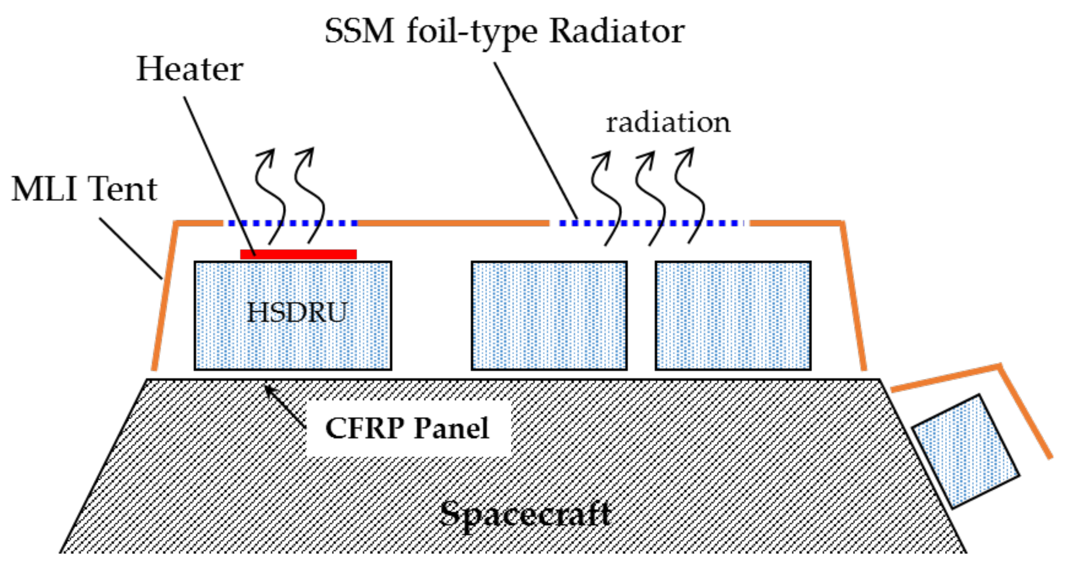
In general, spaceborne electronics are installed on the internal side of sandwich panels of spacecraft. This installation is effective for reducing cosmic ray effects on integrated circuits of electronics. The heat waste of electronics during mission operations is generated by radiation to deep space environments, using radiators attached to the external side of spacecraft panels. Because the external surfaces of a spacecraft with radiators, such as a second surface mirror or thermal-control coatings for various purposes, are radiatively coupled to deep space environments, securing the thermal path from high heat dissipation units to the mounting interface of the electronics is important for the thermal design of electronics installed on the internal side of sandwich panels of spacecraft. This indicates that the bottom side of the electronics conductively couple to the internal panel structure with a radiating area on the outside of the spacecraft’s panel.
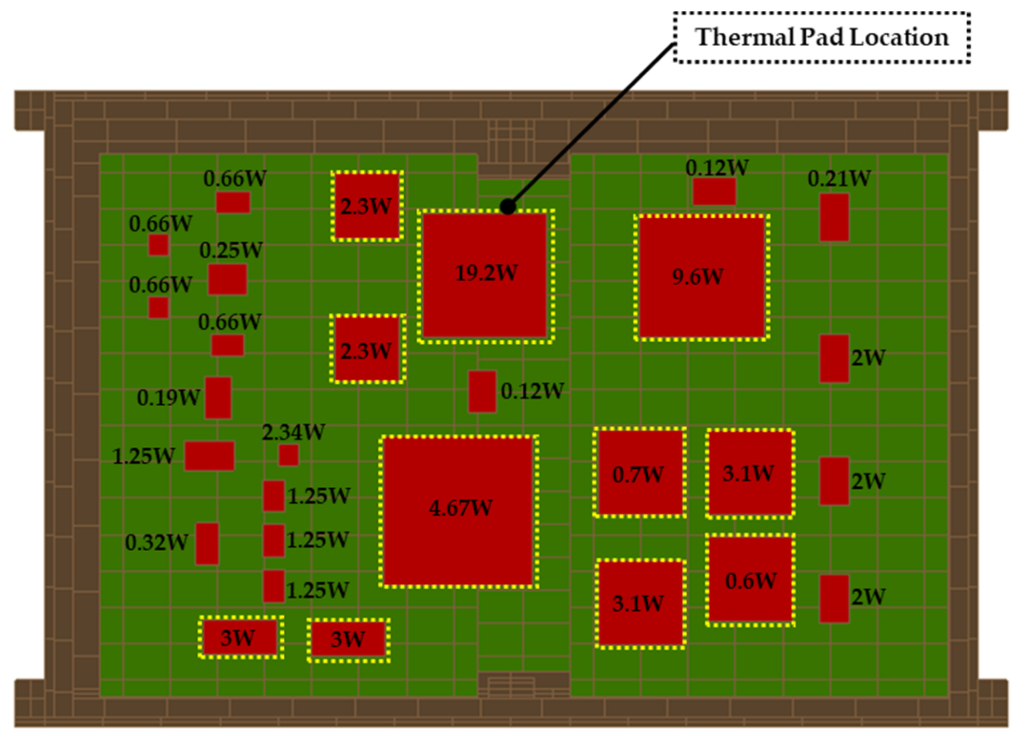
The main features of the high-speed digital receiver unit (HSDRU) developed for spaceborne synthetic aperture radar applications is its mounting position on the spacecraft. It is installed on the external side of a carbon fiber-reinforced panel (CFRP) honeycomb panel structure of spacecraft with low thermal conductivity owing to its mechanical design constraints, which is in contrast to the conventional electronics installed on the internal side of the spacecraft’s panel structure. In addition, an HSDRU has high-heat dissipation units of FPGAs owing to its high-speed signal processing capability. The main heat waste mechanism of electronics during mission operation is achieved by radiation through upper housing surfaces of the electronics because they are coupled with a foil-type radiator installed near the upper housing of electronics. Therefore, a novel thermal design approach is required, in place of the conventional electronics positioned on the internal side of the spacecraft. The thermo-mechanical philosophy of an HSDRU is to apply dual heat sinks with thermal gap pads and secure the heat rejection path to the upper housing of the HSDRU which interfaces with the foil radiator. The heat sink is also adopted as a mechanical stiffener, which contributes to the mass reduction of the HSDRU. In addition, thermal gap pads implemented between the heat sink and heat dissipation components are beneficial in increasing the fatigue life on the solder joint, owing to the restriction of the dynamic response of PCB. In this study, the effectiveness of the design, considering the perspective of heat sinks with additional functions of the mechanical stiffener, was verified via numerical simulation and launch environment vibration tests.

2. Thermo-Mechanical Design of HSDRU

2.1. Main Function of HSDRU

The HSDRU comprises four digital receiver modules (DRX) and two power supplies for HSDRU (PSD), including primary and redundancy modules for DRX and PSD, respectively.
The primary functions of the HSDRU are to control the SAR system and acquire SAR raw data with analog to digital conversion (ADC), data compression, and formatting.
The HSDRU performs the ADC of the received signal. After A/D conversion, the 1st and 2nd low pass filters are used for anti-aliasing. A smart digital filter (SDF) and block adaptive quantization (BAQ) reduce the SAR raw data size. The consultative committee for space data systems (CCSDS) formats and transmits SAR raw data via a channel link.
The key function of the HSDRU is to acquire signals without distortion. Therefore, we demonstrate the performance of IRF analysis of SNR changes in HSDRUs and the final output of SAR raw data before and after launch, and space environment testing is performed.
Figure 1 presents the DRX functional diagram of data processing. The key elements have the following characteristics:
  • ADC: wide-band (300 MHz, each I/Q channel) and high-speed ADC;
  • Low pass filter with decimation (1st, 2nd): adaptable sampling rate according to SAR modes;
  • Decimation/filter: down-sample digitized ADC data by PM ratio;
  • Smart digital filtering: data reduction using sub-band filter bank;
  • Block adaptive quantization: data reduction using re-quantization table;
  • Formatting: CCSDS formatting, including segmentation;
  • CHL framer: parallelized, packetized data for a four-channel link serializer;
  • RFE: radio frequency equipment;
  • DLS: data link subsystem.

2.2. Thermo-Mechanical Design Approach

Figure 2 presents the schematic thermal control strategy of the equipment at a satellite level. The HSDRU mounted on the external side of the CFRP honeycomb panel structure with a low thermal conductivity value of 2.2 W/m-K and 1.6 W/m-K in in-and out-of-plane, respectively, is decoupled in a deep space environment by utilizing a multi-layer insulator (MLI) supported by an MLI tent structure. The area of the upper housing of the HSDRU is radiatively coupled with deep space using a second surface mirror (SSM) foil-type radiator [7] for the heat waste of equipment during its mission operation. The excessive heat waste to deep space through the foil radiator is compensated by an additional heater attached on the upper housing when the electronic device is turned off.
Figure 3 shows a mechanical configuration of an HSDRU for spaceborne synthetic aperture radar applications. The equipment comprises a primary and redundant power supply for the HSDRU (PSD), a digital receiver (DRX), and a mother board unit (MBU). The total mass of the equipment module is 23 kg, and its maximum volume is 340 × 233 × 280 mm3.
Figure 4 illustrates a thermal control strategy for the DRX of an HSDRU. The total heat dissipation of a DRX is approximately 69 W, and its high-power density is 1439 W/m2. This is a relatively high-heat dissipation level compared to that of a PSD with a power density of 617 W/m2. Therefore, the thermal management of a DRX with high-heat dissipating components of FPGAs is crucial for enhancing a high-speed signal processing capability. The primary feature of the DRX thermal design is the use of a dual heat sink mechanism, as illustrated in Figure 4. The heat conduction path from the heat source of components to the upper housing structure, which interfaces the foil radiator, is secured by a heat sink with thermal gap pads [8]. The upper side of heat sink is conductively coupled with the upper housing structure via flexible graphite foil from Sigraflex [9]. To reduce the total mass of unit and guarantee the structural safety on the solder joint of electrical, electronic, and electromechanical (EEE) parts of an HSDRU, the heat sink is designed, such that it functions as a mechanical stiffener to restrict the out-of-plane dynamic displacement of the PCB. Thermal gap pads for effective heat transfer from heat-dissipating components to the heat sink was constructively applied to the design, based on the results of a previous study [10]. The initial contact pressure of thermal pads is an important parameter for enhancing the heat transfer capability. However, this causes stress on the solder joint of the component because of the pad’s inherent resistance to deformation. In a previous study, we verified that PCB specimens with various compression ratios of thermal pads of 0%, 10% and 50% exposed to launch random vibration loads exhibited increased fatigue lives on the solder joint, owing to the inherent damping and restriction on the dynamic displacement of the PCB [10].

2.3. Thermal Analysis and Results

To verify the effectiveness of the thermal design strategy of an HSDRU with high-power density, thermal analysis was performed. Figure 5 illustrates the thermal mathematical model (TMM) of an HSDRU constructed in Thermal Desktop, a CAD-based geometric interface in systems improved numerical differencing analyzer/fluid integrator (SINDA/FLUINT) [11,12]. TMM and the output of RadCAD, which is a module for calculating radiation exchange factors, are analyzed via SINDA/FLUINT.
Figure 6 presents the PCB configuration of a DRX, and the heat dissipation levels of each component are also plotted in the figure. In this figure, the location of thermal gap pad installation points are also presented. The FPGA series exhibits the highest heat dissipation level of 19.2 W. The high-heat dissipation components are positioned near the radiating area of the upper housing, and the thermal pads with 10% contact pressure are integrated on the relatively vibration sensitive packages to reduce the dynamic deflection of the PCB under launch loads, which reflects the development test results for the fatigue life estimation of the CCGA624 package with initial contact pressure of thermal gap pads.
In the thermal analysis, to validate the effectiveness of the heat sink design, thermal analyses with and without heat sinks were performed at a boundary condition with the qualification test level of 55 °C. The parameters applied to the analysis, such as material and thermo-optical properties, are summarized in Table 1. The thermal resistance from case to board can calculated by:
R C B = L k A × 1 N
where R C B ,   L ,   k ,   A ,   and   N denote the calculated thermal resistance value, lead length from case to board, the thermal conductivity of lead material, the cross-sectional area of lead, and the total number of leads, respectively. The thermal resistance values between thermal gap pads and heat sinks were applied by adopting the thermal conductivities of the thermal gap pads. Table 2 shows the material properties of thermal gap pads of THERM-A-GAP G579 [8] with space heritages.
Figure 7 presents one of the representative thermal analysis results of the HSDRU with and without heat sinks. The temperature contour on the PCB indicated that the temperature of the components was significantly attenuated by the heat sink’s design applications. In addition, all components agree with the derating requirements and application rules for EEE electronic components [5,6]. These analysis results indicate that the thermal design strategy proposed in this study is effective for the heat reduction in a DRX with high power density.

2.4. Structural Analysis and Results

The launch environment of electronics is the main mechanical design driver for HSDRUs. To verify the structural safety in the current design of HSDRUs under a launch environment, structural analysis was performed at a qualification test loading condition.
Figure 8 illustrates the finite element model (FEM) of an HSDRU constructed in MSC patran and Nastran to validate the structural safety of an HSDRU under qualification vibration loading test conditions. The FEM comprises 3,127,417 elements, 1118 MPC, 158 lumped masses connected with RBE2 (electronic components), and 6 DOF constraints at the mounting interface of the unit. The six degrees of freedom at the mounting interfaces of an HSDRU are rigidly fixed.
Table 2 summarizes the material properties used in the structural analysis. In addition, to investigate the influence of thermal pads on the mechanical behavior of the PCB, structural analysis was also performed, considering these thermal pads.
Figure 9 presents the modal analysis results of the HSDRU. The first global bending mode of the HSDRU was observed at 338.9 Hz (first Eigen-frequency). A local bending mode of the DRX heat sink was at 775.7 Hz and the DRX PCB was observed at 794 Hz.
To investigate the structural safety of each component on the PCB of DRX under the qualification level of random and shock loading conditions, PCB analysis was performed, based on the conventional Steinberg’s fatigue failure theory [5].
Steinberg’s fatigue failure theory was proposed in the 1970s to determine the structural integrity of electronic component solder joints for vibrations and shocks, and it is still used in the development of space electronic equipment. It provides a design guide, such that if the maximum deflection of PCB is designed below the maximum allowable deflection calculated from empirical equations, it can survive more than 20 million cycles of random vibrations and more than 10 million cycles of sine vibrations.
PCB resonances can produce stress in the electrical lead wires owing to the relative motion between the component body and the PCB. Figure 10 illustrates the relative bending motion in which stress is generated on the lead part of components by the relative behavior of the PCB at the resonance frequency when vibration is applied. In this study, to verify the requirements for all components and calculation of the margin of safety, the maximum displacement of the PCB was calculated, based on Steinberg’s fatigue failure theory, to compare it with the maximum allowable deflection [1,13].
The allowable deflection of each component for random and shock load cases was calculated from following equations:
δ a l l o w = 0.028 d C t r l 0.5   f o r   r a n d o m
δ a l l o w = 0.168 d C t r l 0.5   f o r   s h o c k
where, δ a l l o w is the allowable deflection of PCB;
d 
is the length of the PCB edge parallel to component, mm;
l 
is the length of the electronic component, mm;
t 
is the thickness of PCB, mm;
C
is the constant for the electronic component type;
  • 1.0 for standard DIP and around the wired PGA;
  • 1.26 for side brazed DIP and double-side wired PGA and surface-mounted leaded ceramic chip carriers with J leads or gull wing leads;
  • 1.75 for BGA;
  • 2.25 for LCCC;
  • 0.075 for resistors, capacitors and semiconductors.
r 
is the relative position factor for the component on PCB =   sin π · x X × sin π · y Y
Figure 11 shows location factor of components related to relative position factor.
To evaluate the structural safety of components on the PCB, we applied the following margin of safety (MoS) rule:
MoS = δ a l l o w S F × δ m a x 1 0 ,   S F   i s   1.25
where δ a l l o w , SF, and δ m a x represent the allowable deflection, safety factor, and calculated deflection, respectively. Table 3 and Table 4 present a qualification level of random and shock load cases, respectively.
δ m a x m m = 250 · x m a x ¨ f n 2
x ¨ m a x = 3 · x ¨ r m s = 3 π 2 · Q · U P S D f n · f n
where, x ¨ m a x denotes the estimated maximum acceleration;
  • x ¨ r m s is the RMS acceleration for 1   σ ;
  • Q is the transmissibility of PCB ( f n );
  • U P S D f n is the input PSD relative to f n ;
  • f n is the PCB resonant frequency.
Table 3, Table 4, Table 5 summarizes launch environment mechanical test specifications at qualification levels.
Based on the first Eigen-frequency of the DRX board, 794 Hz, the analysis was conducted by applying C, the chip configuration coefficient of 1.75, and 1.26 and the PCB thickness of 2.2 mm.
Table 6 summarizes the calculated allowable deflection and MoS for each DRX component with thermal pads. The analysis results indicate that all EEE parts of DRX satisfy the design requirements, such that MoS is greater than 0.
Figure 12 presents the components with the minimum MoS in DRX. Table 7 summarizes the dynamic analysis results of DRX with minimum MoS. The minimum MoS of random and shock loads are 1.61, and 8.62, respectively, at the FPGA component in DRX1(P). Minimum MoS occurred on a relatively large and heavy FPGA component, but with a sufficient margin.

3. Launch Environment Test

To validate the effectiveness of the thermo-mechanical design of the HSDRU proposed in this study, launch environment vibration test campaigns such as sine, random and shock tests were conducted at qualification levels described in Table 3, Table 4, Table 5. Figure 13 presents an example of a vibration test set-up in each axis. Vibration input level control was conducted using the average input level control sensors of P1 and P2. The output sensor for checking the dynamic response of the HSDRU was located on the upper housing of the HSDRU. The qualification tests for the random and shock tests were performed according to the specification summarized in Table 3, Table 4, Table 5. The test condition tolerance of the PSD level and overall grms were ±3 dB and ±10%, respectively. In the test, to validate the structural safety of the HSDRU, a resonance survey test (LLSS: low-level sine sweep) was performed at 0.5 g (5~2000 Hz, 2 Oct/min) before and after the test campaign. The success criteria for LLSS are less than 5% in the frequency shift and 20% in the amplitude shift for modes with effective mass greater than 10% [14]. In addition, abbreviated electrical function tests such as power measurement and state transition according to the operation scenario were also conducted before and after the test campaign.
Figure 14 illustrates the dynamic responses to the random vibration test in each axis. A narrow notching profile based on the maximum design load was applied to circumvent the over testing of the proposed HSDRU.
Table 7 presents the frequency, power spectral density (PSD) and grms level of each axis. In the y-axis case, the vibration response in the z-axis is relatively high, which is ascertained to be the structural characteristics of the HSDRU with the first global bending mode in the x axis and stacked module.
The first Eigen-frequencies of the X-, Y-, and Z-axes are 337.5 Hz, approximately 654 Hz, and 1460 Hz, respectively.
The first mode is the global bending mode of the HSDRU about the x-axis. The structural characteristics of the HSDRU with the stacked module and screw-fastened structure resulted in a high vibration response in the z-axis direction during the y-axis test.
The structural integrity of the HSDRU was verified via the low-level sine sweep test. The frequency shift (5%) and amplification shift (20%) requirements were satisfied on all axes. Table 8. Summarizes the Low level sine sweep test results before and after random vibration.
According to the low-level sine sweep test results, the first Eigen-frequency of the x-axis was 359.55 Hz, and the difference was approximately 5.6% compared to that of the modal analysis result, 338.9 Hz.
As illustrated in Figure 3, the basic structure of the HSDRU is a module stacking structure in which several modules are fixed in contact with each other, as well as a structure in which the assembled modules are fixed with a radiation plate at the top. When vibration is introduced via external excitation, vibration energy is dissipated via friction of the coupling surface, and the damping effect is generated by the thermal pad and Sigraflex for heat conduction, according to the fastening strength of the modules and radiating plate. Table 9 and Figure 15 presents the first Eigen-frequency and the change of Q factor calculated via the half power method according to the rise in the vibration level.
In the previous study [10], fatigue life tests and analyses of FPGA (CCGA624 package) according to the thermal pad compression ratios from 0% to 50% were conducted in a random vibration environment of 20 grms by adopting a CCGA624 daisy-chain, which has the same mechanical structure and electrical form/fit [15]. Figure 16 and Figure 17 present the test setup and the results of time histories for daisy-chain resistances for each specimen. The specimens were exposed to the random vibration environment at Table 10. The resistance value of the CG0 specimen rapidly reached a failure of the solder joint after 5.38 min of excitation, but there was no change in CG10 AB (10%) and CG50 (50%). Because the resistance values of the specimens with thermal pads did not vary in 1 h, the CG0 specimen exhibited 73 fractured solder joints, including partially cracked ones during the 20 min of random vibration. However, the other three specimens also exhibited cracks on solder joints, although their resistance values were not varied during the test. This is because the initial compressive static load of the pad maintained the electrical connection of the daisy-chain circuit, despite the crack propagation on the solder joint. However, the number of fractured solder joints of specimens with thermal pads was significantly fewer than that without the pad.
These test results indicate that the initial compressive static load of the pad is more beneficial than the case without a thermal pad in guaranteeing structural safety on the solder joint under a random vibration environment. This is because the initial compression load of the pad applied on the package reduces the dynamic deflection of the PCB, which incurs stress on the solder joint under random vibration excitation.
However, in the tests, the exact time to failure on the solder joints could not be observed from the PCB specimens with thermal pads owing to the difficulty in detecting failure on the solder joint under initial static load of the pad via daisy-chain resistance monitoring. Hence, we predicted the fatigue life on the solder joint of the tested specimens with and without the initial compressive static load of the pad via structural analyses.
For the fatigue life prediction of the solder joints of tested specimens, under conditions of an initial compressive static load of the thermal pad in a random vibration environment, the dynamic responses of these specimens were analyzed via structural analyses, with the random vibration profile specified in Table 10. Figure 18 illustrates the boundary conditions for the structural analysis and the fatigue life on the solder joints.
Owing to the fatigue life analysis of case 1, the predicted time to failure of a solder joint with the thermal pad at 0% was 3.43 min, when 10% of the compression ratio applied was 10.67 min, which was 3.11 times larger than that of the 0%, and when 50% of the compression ratio applied was 29.1 min, which was 8.49 times larger than that of the 0% ratio.
In this study, the development of the DRX of an HSDRU was designed considering the 10% compression ratio specified Table 11 and considering the vibration damping and thermal stress caused by the thermal cycle in space.
The component fatigue life was based on the relative motion between the component and the PCB, because this relative motion produces stresses in the lead wires and solder joints. When stress levels are high, the fatigue life is low, and vice versa. Therefore, the stress levels in the lead wires must be reduced. This can be achieved by increasing the damping and PCB resonance frequency. In the design of the DRX of an HSDRU, a thermal pad and heat sink were applied to increase the damping and resonance frequency of the DRX PCB.
Although the influence of the thermal pad applied to space-grade FPGA (CCGA Package) on the fatigue life improvement cannot be directly observed in these test results, a previous study demonstrated that the fatigue life of solder joints of FPGA was improved by the application of a thermal pad compared to the case without a thermal pad.
Considering Steinberg’s fatigue failure theory [1], the fatigue life of the FPGA of the DRX was estimated to be 6.99 h to fail at a resonance frequency of 794 Hz to apply an MoS of zero. In addition, it is expected that the fatigue lifetime would be further extended by applying a minimum MoS of 1.61, presented in Table 6. The fatigue lifetime to fail is defined as:
TTF Predicted   time   to   failure ,   h = N f f n
where N f is the number of cycles to failure (20 × 106 cycles);
f n is the first Eigen-frequency of PCB.
Using the random vibration test, it was confirmed that the structural integrity of the main electrical components with applied thermal pad to reduce dynamic deflection was also effective.
The abbreviated function test was conducted to verify the electrical requirements of the HSDRU before and after the vibration test. The state transition action test and power consumption test were conducted, and it verified that there was no abnormality in the electrical performance after the vibration test.
The history dump data check and the state transition action test were performed after the x-axis random vibration test.
Figure 19 indicates that the x-axis power consumption is 112.324 W and the power margin is 45.676 W. The test results on the x-axis and confirms that the requirements are satisfied for the rest of the axes.
The shock test demonstrates the ability of the HSDRU to withstand the shocks encountered during its lifetime, such as fairing separation, space segment equipment separation, booster burn out, apogee boost motor ignition, solar arrays, and antenna deployment, as well as shocks from the landing of reusable elements. A shock input profile was derived from the satellite system environmental specification. The HSDRU hardware integrity was assessed via visual inspection and an abbreviated function test.
The shock test was performed using a pyro-shock tester that pressurizes pneumatic pressure and applies impact to the sphere, and the main specifications of the test machine are presented in Table 12.
For shock control, the average value control was performed using two control sensors P1 and P2, and a monitoring sensor was mounted on the top plate of the HSDRU to check the response characteristics of the HSDRU compared to the input shock level. Owing to the characteristics of the pyro-shock tester, the input shock level exceeded the upper limit specification in some frequencies; however, there was no problem in the test because of the worst-case test. It was confirmed that the HSDRU satisfies the shock test requirement in the three axes. Figure 20 and Figure 21 presents the shock test results in the x-axis.
The same abbreviated function test performed during the vibration test was conducted to verify the electrical requirements before and after the shock test. It was confirmed that no abnormality existed in the electrical performance in the three axes after the shock test. Figure 21 indicates the x-axis power consumption was 111.2 W and the power margin was 46.8 W. Test results on the x-axis confirm that the requirements were satisfied for the rest of the axis.
The launch environment tests identified no electrical and mechanical problems, and they verified the design. In addition, although not described in this paper, there were no problems in the thermal vacuum test. Hence, it can be deduced that the proposed heat sink-applied thermo-mechanical design was verified.

4. Conclusions

In this study, a high-speed digital receiver unit, which was mounted on an SAR satellite to acquire raw data for the operation and control for SAR and conduct ADC, data reduction, and formatting SAR output data (CCSDS) was proposed and verified for thermo-mechanical designs by testing via the qualification model.
Unlike conventional electronic equipment, an HSDRU is designed to transfer high-density heat sources from electronic components inside equipment to the top plate through a heat sink to dissipate heat to the deep space. The heat sink functions in dissipating high-density heat and as a stiffener that complements the structural rigidity of the DRX module.
In the case of a package with high-heat generation and relatively large size, based on the results of previous studies, a thermal conductive pad was applied to secure a thermal path and simultaneously, it was actively used to secure the structural integrity and increase the fatigue life of the device, owing to the restriction of the dynamic displacement of PCB under random vibration.
This thermo-mechanical design approach was verified via launch environment and thermal vacuum tests, and it was verified that no abnormality was observed in the primary mechanical/electrical functions.

Author Contributions

Writing—original draft preparation, S.-W.P. and S.-J.K.; writing—review and editing, H.-U.O.; review H.-Y.C., G.-H.R., S.-H.J., J.-P.K. and S.-Y.K., H.-I.L. All authors have read and agreed to the published version of the manuscript.

Funding

This research was funded by Ministry of Science and ICT (MSIT).

Institutional Review Board Statement

Not applicable.

Informed Consent Statement

Not applicable.

Data Availability Statement

The data used to support the findings of this study are available from the corresponding author upon request.

Acknowledgments

This research was supported by the Korea Aerospace Research Institute (KARI) and funded by the Ministry of Science and ICT (MSIT).

Conflicts of Interest

The authors declare no conflict of interest.

References

  1. Steinberg, D.S. Vibration Analysis for Electronic Equipment, 3rd ed.; John Wiley and Sons Inc.: New York, NY, USA, 2000. [Google Scholar]
  2. Ghaffarian, R. CCGA Packages for Space Application. Microelectron. Reliab. 2006, 46, 2006–2024. [Google Scholar] [CrossRef]
  3. Cinar, Y.; Jang, J.; Jang, G.; Kim, S.; Jang, J. Effect of Solder Pads on the Fatigue Life of FBGA Memory Modules under Harmonic Excitation by using A Global-local Modeling Technique. Microelectron. Reliab. 2013, 53, 2043–2051. [Google Scholar] [CrossRef]
  4. Kim, Y.K.; Hwang, D.S. PBGA Packaging Reliability Assessments under Random Vibrations for Space Applications. Microelectron. Reliab. 2015, 55, 172–179. [Google Scholar] [CrossRef]
  5. ESA-ESTEC. Space Product Assurance, Derating–EEE Components; ECSS-Q-ST-30-11C; ESA-ESTEC: Noordwijk, The Netherlands, 2011. [Google Scholar]
  6. NASA. EEE-INST-002: Instructions for EEE Parts Selection, Screening, Qualification, and Derating. NASA/TP-2003-212242; 2008. Available online: https://nepp.nasa.gov/docuploads/FFB52B88-36AE-4378-A05B2C084B5EE2CC/EEE-INST-002_add1.pdf (accessed on 7 May 2021).
  7. Sheldahl. The Red Book. Available online: www.sheldahl.com (accessed on 7 May 2021).
  8. Chomerics. CHO-THERM, Thermally Conductive Elastomer Insulator. Available online: www.chomerics.com (accessed on 7 May 2021).
  9. SGL Carbon. Sigraflex Standard. Available online: www.sigraflex.com (accessed on 7 May 2021).
  10. Park, T.Y.; Jeon, S.H.; Kim, S.J.; Jung, S.H.; Oh, H.U. Experimental Validation of Fatigue Life of CCGA 624 Package with Initial Contact Pressure of Thermal Gap Pads under Random Vibration Excitation. Int. J. Aerosp. Eng. 2018, 2018, 2697516. [Google Scholar] [CrossRef]
  11. Panczak, T.D.; Ring, S.G.; Welch, M.J.; Johnson, D.; Cullimore, B.A.; Bell, D.P. Thermal Desktop User’s Manual; C&R Technologies: Boulder, CO, USA, 2008. [Google Scholar]
  12. Michael, F.M. Radiative Heat Transfer, 2nd ed.; The Academic Press: Cambridge, MA, USA, 2003. [Google Scholar]
  13. Jeong, S.Y.; Oh, H.O. Mechanical Stability Analysis of PCB and Component for Launch and On-orbit Environment based on Fatigue Failure Theory and FEM. Korean Soc. Aeronaut. Space Sci. 2011, 39, 952–958. [Google Scholar]
  14. ESA. Space Engineering, Testing; ECSS-E-ST-10-03C; ESA: Noordwijk, The Netherlands, 2012. [Google Scholar]
  15. Available online: https://www.microsemi.com/document-portal/doc_view/129892-ac190-ceramic-column-grid-array-application-note (accessed on 17 May 2021).
Figure 1. Functional diagram of data processing for DRX.
Aerospace 08 00305 g001
Figure 2. Schematic of thermal control strategy of HSDRU on spacecraft.
Aerospace 08 00305 g002
Figure 3. Mechanical configuration and exploded view of HSDRU.
Aerospace 08 00305 g003
Figure 4. Schematic diagram of the thermal control strategy of DRX and HSDRU.
Aerospace 08 00305 g004
Figure 5. TMM of HSDRU.
Aerospace 08 00305 g005
Figure 6. DRX internal configuration with heat dissipation and thermal pad location.
Aerospace 08 00305 g006
Figure 7. Temperature contours of DRX1(P) with and without heat sink.
Aerospace 08 00305 g007
Figure 8. FEM of HSDRU.
Aerospace 08 00305 g008
Figure 9. Modal analysis results of HSDRU. (a) First 338.9Hz (global bending mode). (b) Sixteenth 775.7 Hz (local mode, DRX heat sink).
Aerospace 08 00305 g009
Figure 10. Relative bending motion between components and PCB.
Aerospace 08 00305 g010
Figure 11. Location factor of component related to relative position factor of package.
Aerospace 08 00305 g011
Figure 12. Component with minimum MoS in DRX.
Aerospace 08 00305 g012
Figure 13. Vibration test configuration and accelerometer position of HSDRU.
Aerospace 08 00305 g013
Figure 14. Random vibration test results of HSDRU about X-, Y-, and Z-axes.
Aerospace 08 00305 g014aAerospace 08 00305 g014b
Figure 15. Random vibration test results 0 dB and −9 dB of HSDRU.
Aerospace 08 00305 g015
Figure 16. Random vibration fatigue test setup [10].
Aerospace 08 00305 g016
Figure 17. Time profiles of daisy-chain resistance for each specimen [10].
Aerospace 08 00305 g017
Figure 18. Numerical fatigue life prediction on solder joint [10]. (a) Boundary conditions for structural analysis. (b) 1st Eigen-frequency of the PCB for the compression ratio of the thermal gap pad in each case. (c) Fatigue life on solder joint for CCGA624 package with respect to the fatigue life in each case.
Aerospace 08 00305 g018
Figure 19. x-axis power consumption test results after x-axis random vibration test.
Aerospace 08 00305 g019
Figure 20. x-axis shock test results of HSDRU.
Aerospace 08 00305 g020
Figure 21. x-axis power consumption test results after x-axis shock test.
Aerospace 08 00305 g021
Table 1. Material and thermo-optical properties applied to the thermal analysis of DRX.
ComponentThermal Conductivity
(W/m-K)
Density
(kg/m3)
Specific Heat
(J/kg-K)
Al6061-T6167.902680.0961.2
Polyimide
(PCB)
47.10(in-plane)
0.24(through-plane)
1600539.08
Thermal pad
(t = 1.0 mm)
1.79
(under 10% compression)
32001000.0
Sigraflex
(t = 0.254 mm)
250 (in-plane)
5(through-plane)
1000700.0
Table 2. FEM material properties of HSDRU.
MaterialYoung’s Modules
(GPa)
Poisson
Ratio
Density
(kg/m3)
Yield Strength
(MPa)
Ultimate Strength
(MPa)
AL6061-T668.90.332700276310
Polyimide
(PCB)
26.20.151600-250
Table 3. Qualification random vibration load case. (Duration is 2 min).
Frequency (Hz)Acceleration PSD (g2/Hz)
PSD Profile200.032
500.2
8000.2
20000.06
Overall grms 16.8
Table 4. Qualification sine vibration load case.
X and Y AxesZ AxisSweep Rate
Frequency (Hz)Acceleration (g)Frequency (Hz)Acceleration (g)
5~209.3 mm5~2011 mm2 Oct/min
20~751520~7520
75~100675~1006
Table 5. Qualification shock load case.
Table SpectrumFrequency (Hz)Acceleration (g)Axis
Q = 103063 Axis
2 x each Axis
1000500
10,000500
Table 6. Dynamic analysis results of DRX of HSDRU with minimum MoS.
ModuleComp.Ct
(mm)
l
(mm)
d
(mm)
r δ a l l o w δ m a x MoS
RandomShockRandomShockRandomShock
DRX1
(P)
11.752.240153.50.5410.331.960.10.161.618.62
21.262.248153.50.8270.271.620.080.161.716.98
DRX2
(P)
31.262.248153.50.8270.271.620.080.162.8811.14
Table 7. Random vibration test results of each axis.
Axis1st Frequency (Hz)PSD Peak
(g2/Hz)
grmsQ Factor
XYZ
x-axis337.531.1441.539.7413.6811.68
y-axis6542.048.0131.8621.45-
z-axis14603.7414.9111.8733.82-
Table 8. Low-level sine sweep test results before and after random vibration.
AxisTestFrequency (Hz)Amp.
Factor (g)
Freq.
Shift (%)
Amp.
Shift (%)
XBefore Random359.5530.42
After Random357.4531.62−0.593.80
YBefore Random875.7413.04
After Random875.7413.970.006.66
ZBefore Random1610.3014.94
After Random1610.3014.180.00−5.36
Table 9. First frequency and Q factor change according to the rise of vibration level.
Random Vibration Level1st Frequency (Hz)PSD (g2/Hz)Q FactorDamping Ratio
0 dB337.531.1411.684.3%
−9 dB356.35.93321.842.3%
Table 10. Specification of random vibration [10].
Frequency (Hz)PSD (g2/Hz)
200.404
20000.404
Overall28 grms
Table 11. Abbreviated function test.
Test ItemRequirements
State Transition ActionHistory Dump Data check
State transition and anomaly check:
Achieved State: INIT/STANDBY/PREOP/SILENT/OP/SILENT/PREOP/STANDBY/INIT
Power ConsumptionMax Power Consumption check
OFF/INIT/STNDBY: 0 W
PRE-OP/SILENT: 136 W
OPERATION (30%/20%/10%): 158 W
Table 12. Specification of vertical pyro-shock test machine.
Frequency (Hz)Specification
Driving methodCompressed air
Interface area1 m × 1 m
Weight of test object100 kg
Test Specification2000 g SRS at 1.5 kHz
Publisher’s Note: MDPI stays neutral with regard to jurisdictional claims in published maps and institutional affiliations.

