Article

A Modified Criss-Cross-Based T-Type MLI with Reduced Power Components

1
Department of Electrical Engineering, National Institute of Technology, Agartala 799046, India
2
Department of Electrical and Electronics Engineering, Galgotias College of Engineering & Technology, Greater Noida 201310, India
3
Department of Electrical Engineering, Indian Institute of Technology (Indian School of Mines), Dhanbad 826004, India
4
Department of Electrical and Electronics Engineering, Gaya College of Engineering, Gaya 823003, India
5
Department of Electrical and Electronics Engineering Educators, ASPETE—School of Pedagogical and Technological Education, 14121 Heraklion, Greece
6
Hellenic Air Force Academy, Dekelia Air Base, Acharnes, 13671 Athens, Greece
7
Centre for Energy Technologies, Aarhus University, Birk Centerpark 15, Innovatorium, 7400 Herning, Denmark
*
Authors to whom correspondence should be addressed.
Technologies 2024, 12(6), 90; https://doi.org/10.3390/technologies12060090
Submission received: 29 March 2024 / Revised: 31 May 2024 / Accepted: 12 June 2024 / Published: 18 June 2024
(This article belongs to the Collection Electrical Technologies)

Abstract

:
Significant advancements in the field of power electronics have created an ideal opportunity to introduce various topologies of multilevel inverters. These multilevel inverter topologies comprise different notable characteristics, such as staircase sinusoidal output voltage with high quality, a lowered number of power switches, no filter requirement, etc. In this literature, a new asymmetrical MLI topology is proposed to reduce the number of components of the inverter with admirable voltage-step creation. The proposed topology provides a 17-level, staircase-type, nearly sinusoidal output voltage waveform. The number of switches required for the proposed multilevel inverter topology is fewer compared to the existing topology for the same level. A carrier-based sinusoidal pulse-width modulation technique is used for the proposed topology at a switching frequency of 3 kHz. The functioning of the proposed inverter topology is thoroughly examined. A 17-level asymmetrical inverter is executed; both the MATLAB/SIMULINK as well as the experimental results using dSPACE-1103 controller. The simulation results are verified using the experimental results for the proposed 17-level multilevel inverter for modulation indexes of 1 and 0.6.

1. Introduction

Currently, researchers are directing their attention towards multilevel inverters (MLIs) within the realm of power electronics for a number of reasons. MLIs hold significant sway in power electronics converters due to their numerous applications and associated advantages [1]. Conventional inverters encounter challenges related to waveform quality, switching frequency, and electromagnetic interference (EMI). However, these issues are mitigated in MLIs, as MLIs offer enhanced features for instance superior quality staircase sinusoidal output voltage with reduced total harmonic distortion (THD), a reduced requirement for power switches, and the elimination of the necessity for extra filters [2,3]. MLIs offer improved solutions in diverse applications like high-voltage DC power transmission, electric vehicles, and variable-frequency devices due to their superior features [4,5,6]. Given the numerous constraints, the world is increasingly turning to renewable energy resources. MLIs also prove beneficial in renewable energy power conversion systems, such as those utilizing solar energy and wind energy. MLIs are highly suitable for applications requiring high power and medium voltage. Multilevel inverters (MLIs) have a wide range of applications across various industries due to their ability to generate high-quality AC waveforms with reduced harmonic distortion. Some common applications of MLIs include the following:
(I).
Renewable energy systems: MLIs are widely used in renewable energy systems such as solar photovoltaic (PV) inverters and wind turbine generators for grid integration. They help convert the DC power generated by renewable sources into grid-compatible AC power with improved efficiency and power quality [7,8].
(II).
Motor drives: MLIs are employed in adjustable speed motor drives for controlling the speed and torque of electric motors used in industrial and commercial applications. They provide smoother operation and higher efficiency compared to traditional two-level inverters [9]
(III).
Grid-tied inverters: MLIs are utilized in grid-tied inverters for feeding power from distributed energy resources (DERs) such as solar panels or batteries into the electrical grid. They enable precise control of power flow and support functions like reactive power compensation and voltage regulation [10,11].
(IV).
High-voltage direct current (HVDC) transmission: MLIs are used in HVDC transmission systems for converting AC power to DC power at the sending end and vice versa at the receiving end. They help improve the efficiency and stability of long-distance power transmission [12].
(V).
Electric vehicles (EVs): MLIs play a crucial role in the power electronics systems of electric and hybrid vehicles, converting DC power from batteries or fuel cells into AC power for driving motors. They enable efficient energy conversion and regenerative braking [13,14].
Utilizing multiple DC inputs, MLIs produce a staircase-like output voltage, which closely resembles a sinusoidal waveform, thus minimizing total harmonic distortion [15]. As a result, the need for filters is significantly diminished. Furthermore, the staircase voltage output reduces the dv/dt ratio.
The flying capacitor-based MLI (FC-MLI) was introduced by Dickerson and Ottaway [16] in the US patent filed in December 1969 and granted in 1971. For developing a high-power converter like an FC-MLI, Meynard and Foch [17] introduced a new versatile commutation cell in 1992, with an objective to enable voltage sharing and zero harmonics at switching frequency. The switching circuit and bridge converter circuit [18] for the NPC-MLI (also known as the diode clamped MLI) were filed as a US patent by Baker et al. in 1978 and 1980, being granted in July 1980 and May 1981, respectively. In [19], Nabae et al. developed a three-level neutral point clamped (3L-NPC) inverter. In July 1969, McMurray filed a US (United States) patent [20], granted in 1971, with the objective of providing a new and improved switching power converter circuit (now popularly known as a cascaded H-bridge inverter) that could generate a stepped-wave output voltage. Moreover, another US patent [21] was filed by Baker and Bannister in 1974 for a cascaded H-bridge inverter, granted in 1975.
Although traditional MLIs provide numerous benefits compared to two-level inverters, they also have drawbacks such as the need for a large quantity of power switches. In certain cases, multiple DC voltage sources and capacitors are required. Due to the lower total standing voltage in the recent MLI presented by researchers utilizing lower-rated semiconductor switches, resulting in cost savings to overcome these challenges, numerous new MLI topologies have been proposed with the aim of reducing components and enhancing efficiency. These topologies can be categorized into symmetrical and asymmetrical groups on the basis of the magnitude of the input voltage sources used in the MLI [22,23,24]. Symmetrical MLIs have uniform input voltage magnitudes, whereas asymmetrical MLIs show variations in input voltage magnitudes.
The MLI topology proposed was simulated using sinusoidal pulse-width modulation (SPWM) on the MATLAB/Simulink platform. Following this, an experimental prototype of the multilevel inverter was built in a laboratory, utilizing a dSPACE-1103 controller to validate the simulation result and illustrate its performance at a switching frequency of 3 kHz. This paper is organized into four sections, covering the modulation and control of the MLI in Section 2 and the operation of the proposed topology in all modes in Section 3. Section 4 compares the proposed topology with other existing MLI topologies. Section 5 discusses the simulation parameters and desired outputs, followed by a conclusion provided in Section 6.

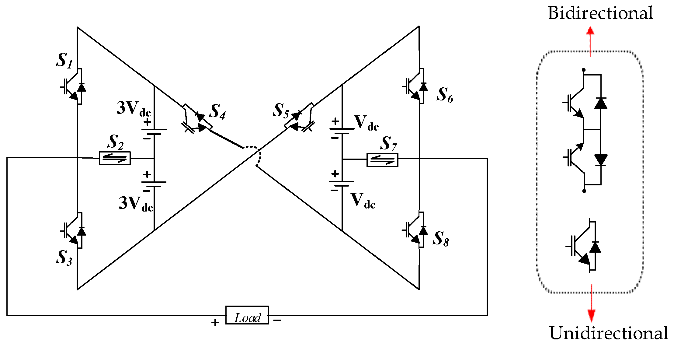
2. Proposed Circuit Topology

The proposed 17-level inverter topology, depicted in Figure 1, comprises thirteen switches labelled from S1 to S8, including two bidirectional switches (S2 and S7) and six unidirectional switches (S1, S3, S4, S5, S6, and S8). The unidirectional switches operate across two quadrants whereas the bidirectional switches operate across four quadrants. This configuration utilizes four isolated DC sources, 3Vdc, 3Vdc, Vdc, and Vdc, operating in an asymmetrical mode. Without utilizing an H-bridge at the output, these asymmetric sources and switch configurations provide distinct pathways for producing positive and negative 17-level bipolar output voltage. The specified magnitude for the isolated DC sources is Vdc = 39 V and 3Vdc = 117 V.
Three distinct configurations of bidirectional switches are well presented in [25] and can be explained as follows:
(I).
Common emitter configuration: This configuration utilizes an insulated gate bipolar transistor in a common emitter configuration. The common emitter setup involves the emitter terminal being common between the input and output circuits. In this arrangement, the IGBT serves as the main switching element, controlling the flow of current bidirectionally, as depicted in Figure 2a.
(II).
Power switch with four-diode configuration: This configuration incorporates a diode bridge switch. A diode bridge consists of four diodes arranged in a bridge configuration, allowing for current to flow bidirectionally. However, this setup typically involves more diodes compared to other configurations, potentially leading to higher conduction losses, as depicted in Figure 2b.
(III).
Common collector configuration: This configuration employs an IGBT in a common collector setup. In a common collector arrangement, the collector terminal serves as the common connection point between the input and output circuits. Here, the IGBT controls the current flow bidirectionally while providing a different configuration compared to the common emitter setup as depicted in Figure 2c.
Figure 2. Different types of configurations for bidirectional switches: (a) common emitter configuration; (b) power switch with four-diode configuration; (c) common collector configuration.
Technologies 12 00090 g002

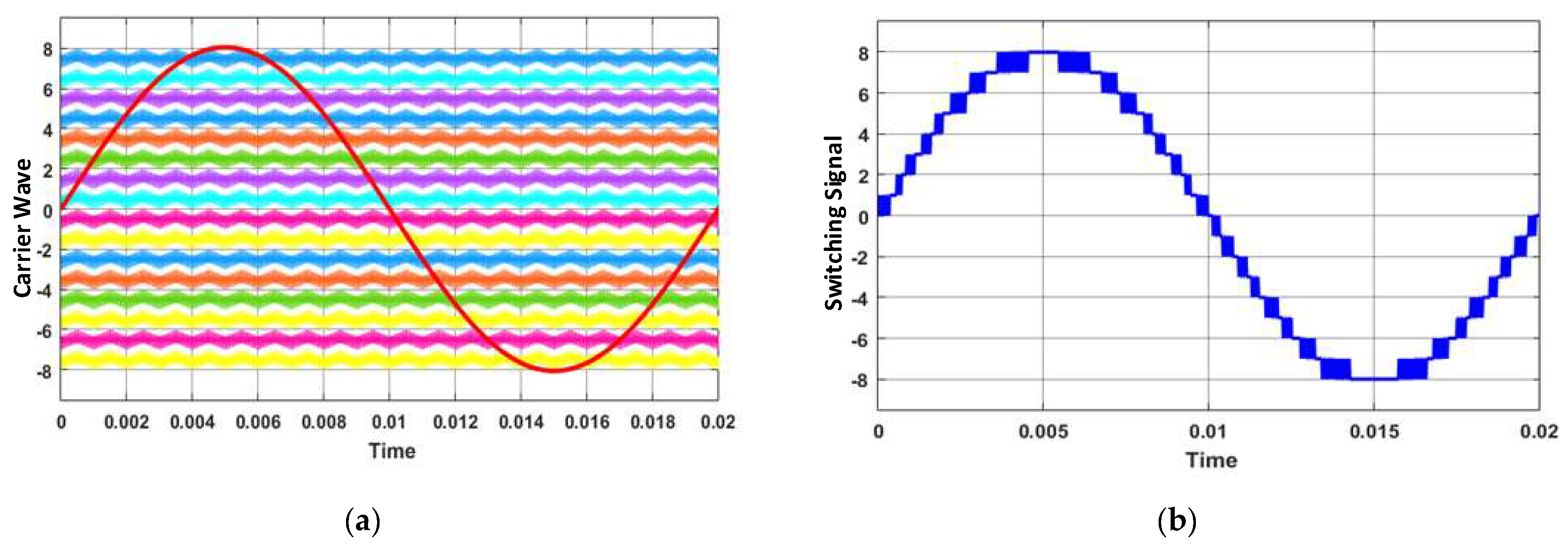
Modulation and Control of MLI

Many control modulation strategies have been presented by the researchers, including carrier-based pulse-width modulation, selective harmonic elimination (SHE), nearest level control, and space vector pulse-width modulation (SVPWM) [26,27,28]. Modulation techniques are essential for improving the efficiency of MLIs by minimizing switching losses, optimizing voltage and current waveforms [29]. In this study, the SPWM control modulation technique was used to produce the switching signal for a 17-level inverter, as depicted in Figure 3a. A carrier-based PWM modulator consists of both modulation signals and a carrier signal. The reference signal is represented by the red line which is typically a sine wave. The carrier signals are represented by different colors as triangular waves or sawtooth waves. Multiple carriers are shown, each in a different color. These carriers are compared with the reference signal to generate the PWM signals. To generate a switching signal for the 17-level inverter, 16 triangular carrier waveforms are utilized. The digital output is produced by continually comparing the carrier signals with the reference signal using sixteen comparators. As shown in Figure 3b, the sixteen output signals of the comparator were aggregated to create the inverter switching signal. The generated switching signal for a single-phase, 17-level inverter is depicted in Figure 3b along with the accompanying real-time simulation result. Further decoding of the switching signals yields the gate pulses for the relevant switching devices of the proposed MLI.

3. Modes of Operation

The different modes of voltage generation for the 17-level inverter are illustrated in Figure 4. The positive half-cycle voltage generation path of the proposed topology is represented by the red line while the negative half-cycle is represented by the blue one.
The working of the 17-level inverter is elucidated below:
  • Switches S1, S5, and S8 are activated to produce +8Vdc, as illustrated in Figure 4a, while S3, S4, and S6 are turned ON to generate −8Vdc.
  • The power switches S1, S5, and S7 are turned ON to generate +7Vdc, as illustrated in Figure 3b, whereas S3, S4, and S7 are activated to generate −7Vdc.
  • Switches S1, S5, and S6 are activated to achieve +6Vdc, as illustrated in Figure 4c, whereas S3, S4, and S8 are turned ON to generate −6Vdc.
  • Switches S2, S5, and S8 are turned ON to achieve +5Vdc, as illustrated in Figure 4d, whereas S2, S4, and S6 are turned ON to generate −5Vdc.
  • Switches S2, S5, and S7 are turned ON to achieve +4Vdc, as illustrated in Figure 4e, whereas S2, S4, and S7 are turned ON to generate −4Vdc.
  • Switches S2, S5, and S6 are turned ON to achieve +3Vdc, as illustrated in Figure 4f, whereas S2, S4, and S8 are activated to generate −3Vdc.
  • Switches S3, S8, and S5 are turned ON to achieve +2Vdc, as illustrated in Figure 4g, whereas S1, S4, and S6 are activated to generate −2Vdc.
  • Switches S2, S5, and S7 are activated to generate +Vdc, as illustrated in Figure 4h, whereas S1, S4, and S7 are activated to produce −Vdc.
  • Switches S3, S5, and S6 are activated to produce 0Vdc.
The switching mode of the proposed 17-level inverter have been shown in Table 1. The use of green (√) and red (×) symbols signifies the states of switches within the inverter circuit. When a switch position is marked with a green check mark (√), it indicates that the corresponding switch is in the “on” state. Conversely, when a switch position is marked with a red cross (×), it indicates that the switch is in the “off” state.

4. Comparative Study

In recent years, several newly developed MLI configurations have been introduced and analyzed in the various literature [30,31,32,33,34,35,36]. These analyses typically focus on different performance metrics, including the total number of power switches, input DC sources, and capacitors, as well as main diodes. Table 2 presents generalized formulas for these different MLI topologies proposed in the literature, where Z represents the number of output voltage levels of proposed topologies. For a specific example, such as a 17-level inverter, the relevant references are compiled in Table 3. The quantity of required gate driver circuits is equivalent to the quantity of switches utilized, as each switch necessitates one gate pulse for operation. Main diodes are those connected with the switches; a unidirectional switch typically involves one anti-parallel diode, while a bidirectional switch may have two or four associated diodes.
A comprehensive analysis and comparison was carried out with recently introduced topologies [30,31,32,33,34,35,36]. The circuits of the compared manuscript is depicted in Figure 5. In Table 3, a comparative study is shown for the 17-level output. From the comparative study, it can be concluded that the required total number of switches for the proposed MLI is the least compared to the other cited topologies. This reduction in the number of power switches not only simplifies construction but also enhances the control and reliability of the system, making it cost-effective. This can be considered as the advantage of the proposed topology.

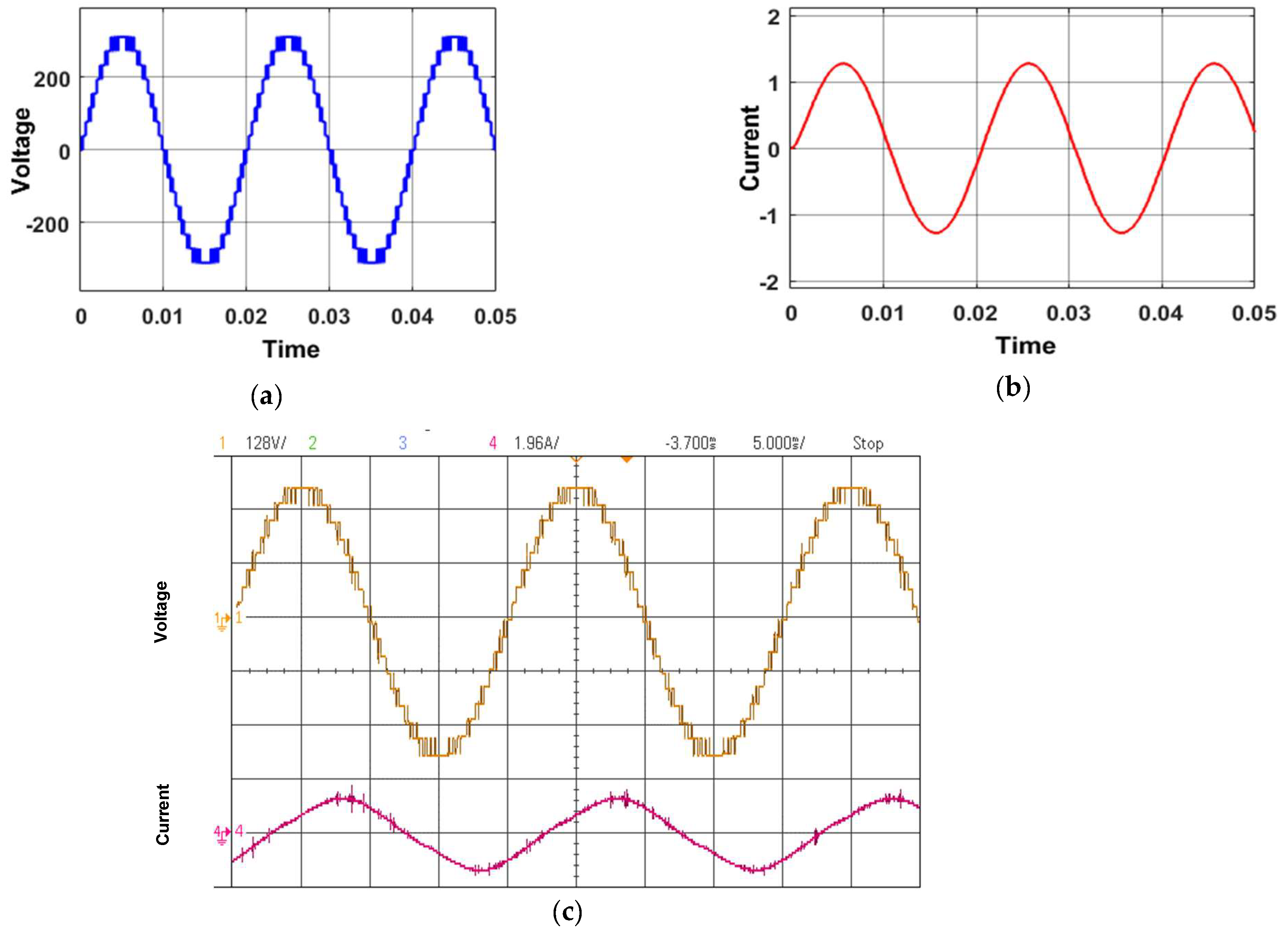
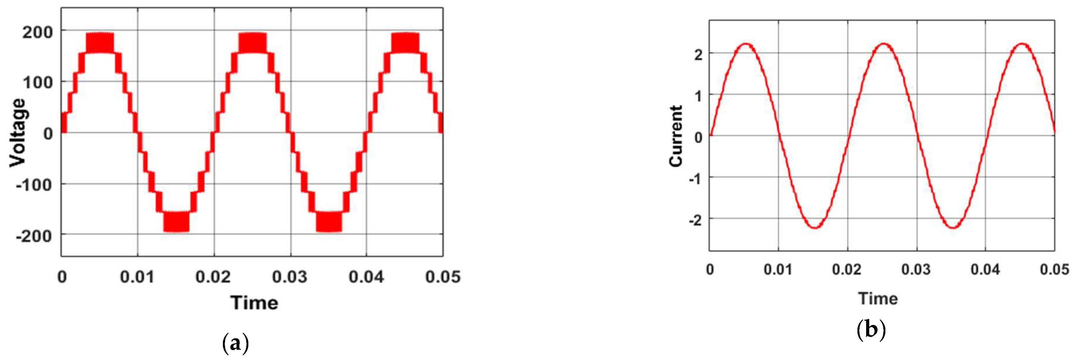
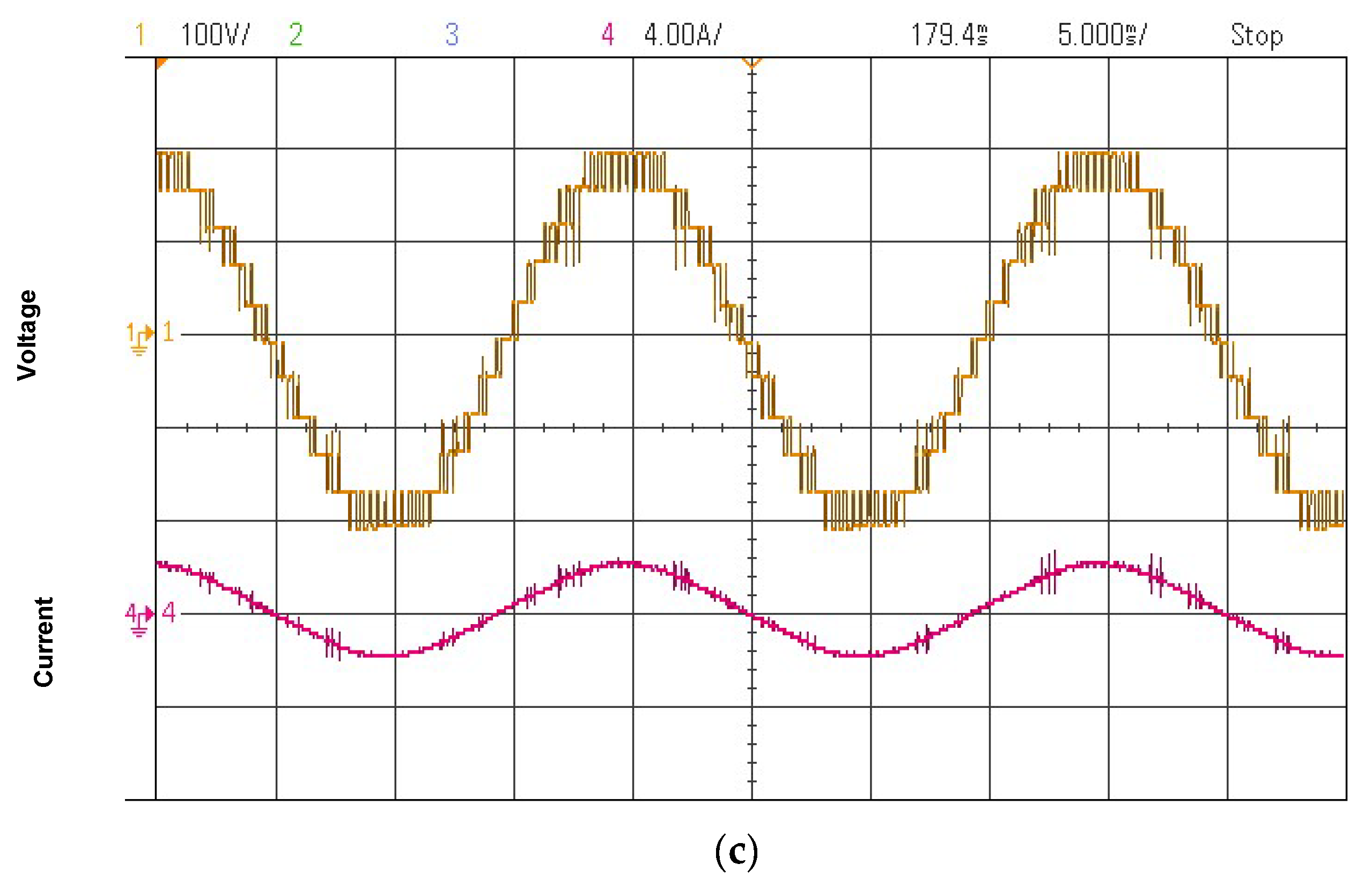
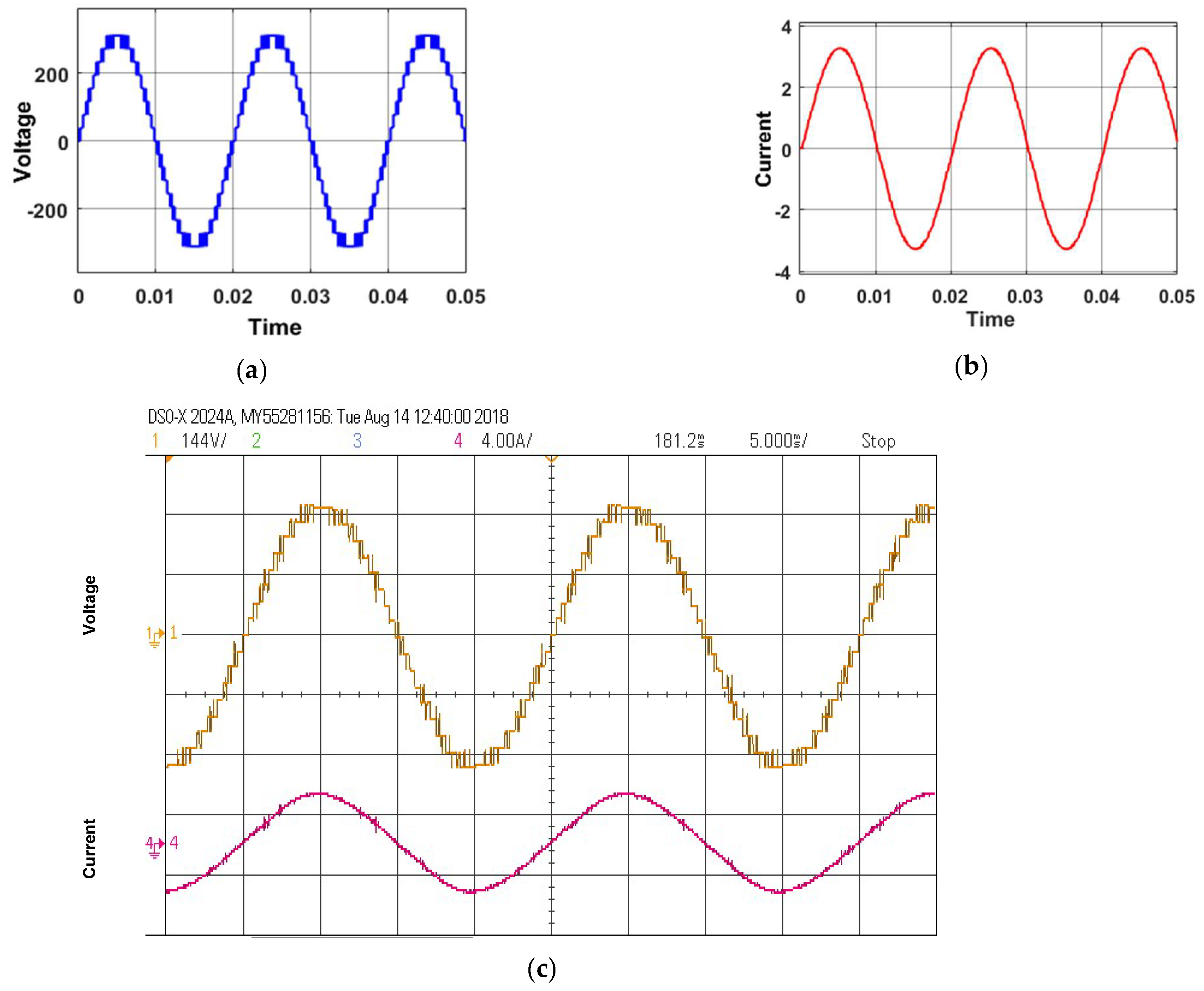
5. Simulation and Experimental Result

The proposed MLI topology was simulated, employing level-shifted SPWM on the MATLAB/Simulink platform. Subsequently, a prototype model of the MLI was constructed in a laboratory, employing a dSPACE-1103 controller. The components utilized in this prototype model include power switches (IGBT-CT60AM), gate driver circuits (TLP250), isolated DC sources, a DSO-X 2024A oscilloscope, and an RL load, as illustrated in Figure 6.
The blocking voltage in an MLI is critical for ensuring the reliability and safety of the circuit. It refers to the voltage rating that each switching device must withstand when in the off state. Overvoltage leads to semiconductor device failure and potentially damages the entire inverter circuit. Therefore, selecting switching devices with appropriate voltage ratings is crucial in MLI design to ensure dependable and safe operation. The blocking voltages across the switches S1, S2, S3, S4, S5, S6, S7, and S8 are as follows: 250 V, 120 V, 225 V, 78 V, 40 V, 78 V, 305 V, and 305 V, respectively, as depicted in Figure 7.
The simulation and experimentation were performed for the proposed 17-level inverter with two distinct loads: one with R = 180 Ω, L = 150 mH, and the other with R = 180 Ω, L = 25 mH at modulation index (MI) 0.6 and 1. The input volage values were V1 = V2 = 39 V and V3 = V4 = 117 V, as detailed in Table 4, with the output voltage and load current.
The simulation results for the proposed 17-level inverter at MI = 0.6 are illustrated in Figure 8. The simulation was conducted with an RL load, where R = 180 Ω and L = 150 mH. The input voltage parameters were set to Vdc = 39 V and 3Vdc = 117 V, as per the proposed topology. In Figure 8a, the simulation output voltage (Vo/p max) is shown to be 196 V. Similarly, in Figure 8b, the load current (Io/p max) is measured at 0.78 A for the same input DC voltage. The experimental result validates the simulation results of output voltage and load current, as shown in Figure 8c.
The performance analysis of the proposed 17-level inverter is conducted with the same set of loads where (R = 180 Ω and L = 150 mH) and input voltage (Vdc = 39 V and 3Vdc = 117 V) at MI = 1. Results from both simulations and experiments are depicted in Figure 9. In Figure 9a, the simulation result shows an output voltage of 320 V. Correspondingly, in Figure 9b, the load current is measured at 1.4 A. Furthermore, the simulation results for the output voltage and load current at MI = 1 were validated by the experimental data, as depicted in Figure 9c.
The simulation and experimentation were performed for the proposed 17-level inverter with the loads R = 90 Ω, L = 25 mH at MI = 0.6. The input volage values were V1 = V2 = 39 V and V3 = V4 = 117 V. The simulation output voltage (Vo/p max) was 196 V, as depicted in Figure 10a, and the load current was 1.8 A, as depicted in Figure 10b. The experimental result for the output voltage and the load current is shown in Figure 10c, which validates the simulation result.
The simulation and experimentation were performed with the loads R = 90 Ω, L = 25 mH at MI = 1 for the input volage values V1 = V2 = 39 V and V3 = V4 = 117 V. The simulation output voltage (Vo/p max) was 320 V, as depicted in Figure 11a, and the load current was 2.4 A, as depicted in Figure 11b. The output voltage and load current observed experimentally as depicted in Figure 11c aligned closely with the simulation results, further validating the effectiveness and accuracy of the proposed 17-level inverter.

6. Conclusions

This paper introduced a new criss-cross-based T-type MLI topology for 17-level output voltage. A comparative study was conducted with the proposed MLI topology. The number of switches required to generate 17-level voltage output is fewer compared to the other compared topologies. The reduction in the number of components makes the proposed topology cost-effective. All the simulation results were validated with a hardware result designed in the laboratory. The future scope of the proposed topology is broad and promising, driven by ongoing advancements in power electronics and renewable energy systems. Some potential avenues for development include investigating its fault-tolerance capabilities, reliability improvement, efficiency enhancement, and its application in motor vehicle and renewable energy systems as an efficient power converter. The limitation of the proposed topology is that it has to be modified on the basis of its application. It is complex in terms of its control strategies and circuit design.

Author Contributions

Methodology, B.M.; Software, K.K.M.; Formal analysis, D.D. and C.P.; Investigation, P.D.; Resources, D.D., G.F. and S.K.; Data curation, B.C.; Writing—review & editing, B.C. and V.V.; Supervision, B.M. All authors have read and agreed to the published version of the manuscript.

Funding

This research received no external funding.

Informed Consent Statement

Not applicable.

Data Availability Statement

The data presented in this study are available in this article.

Conflicts of Interest

The authors declare no conflict of interest.

References

  1. Bana, P.R.; Panda, K.P.; Naayagi, R.T.; Siano, P.; Panda, G. Recently developed reduced switch multilevel inverter for renewable energy integration and drives application: Topologies, comprehensive analysis and comparative evaluation. IEEE Access 2019, 7, 54888–54909. [Google Scholar] [CrossRef]
  2. Gupta, K.K.; Ranjan, A.; Bhatnagar, P.; Sahu, L.K.; Jain, S. Multilevel Inverter Topologies with Reduced Device Count: A Review. IEEE Trans. Power Electron. 2016, 31, 135–151. [Google Scholar] [CrossRef]
  3. Veenstra, M.; Rufer, A. Control of a hybrid asymmetric multilevel inverter for competitive medium-voltage industrial drives. IEEE Trans. Ind. Appl. 2005, 41, 655–664. [Google Scholar] [CrossRef]
  4. Chakraborty, A. Advancements in power electronics and drives in interface with growing renewable energy resources. Renew. Sustain. Energy Rev. 2011, 15, 1816–1827. [Google Scholar] [CrossRef]
  5. Mahato, B.; Jana, K.C.; Thakura, P.R. Constant V/f control and frequency control of isolated winding induction motor using nine-level three-phase inverter. Iran. J. Sci. Technol. Trans. Electr. Eng. 2019, 43, 123–135. [Google Scholar] [CrossRef]
  6. Shahin, A.; Hinaje, M.; Martin, J.-P.; Pierfederici, S.; Rael, S.; Davat, B. High voltage ratio DC-DC converter for fuel-cell applications. IEEE Trans. Ind. Electron. 2010, 57, 3944–3955. [Google Scholar] [CrossRef]
  7. Agrawal, R.; Jain, S. Multilevel inverter for interfacing renewable energy sources with low/medium- and high-voltage grids. IET Renew. Power Gener. 2017, 11, 1822–1831. [Google Scholar] [CrossRef]
  8. Yadav, D.; Singh, N.; Bhadoria, V.; Vita, V.; Fotis, G.; Tsampasis, E.G.; Maris, T.I. Analysis of the Factors Influencing the Performance of Single- and Multi-Diode PV Solar Modules. IEEE Access 2023, 11, 95507–95525. [Google Scholar] [CrossRef]
  9. Somasekhar, V.T.; Gopakumar, K.; Baiju, M.R.; Mohapatra, K.K.; Umanand, L. A multilevel inverter system for an induction motor with open-end windings. IEEE Trans. Ind. Electron. 2005, 52, 824–836. [Google Scholar] [CrossRef]
  10. Mahto, K.K.; Pal, P.K.; Das, P.; Mittal, S.; Mahato, B. A New Design of Multilevel Inverter Based on T-Type Symmetrical and Asymmetrical DC Sources. Iran. J. Sci. Technol. Trans. Electr. Eng. 2023, 47, 639–657. [Google Scholar] [CrossRef]
  11. Maris, T.I.; Kourtesi, S.; Ekonomou, L.; Fotis, G. Modeling of a single phase photovoltaic inverter. Sol. Energy Mater. Sol. Cells 2007, 91, 1713–1725. [Google Scholar] [CrossRef]
  12. Kala, P.; Arora, S. A comprehensive study of classical and hybrid multilevel inverter topologies for renewable energy applications. Renew. Sustain. Energy Rev. 2017, 76, 905–931. [Google Scholar] [CrossRef]
  13. Gritter, D.; Kalsi, S.S.; Henderson, N. Variable speed electric drive options for electric ships. In Proceedings of the IEEE Electric Ship Technologies Symposium, Philadelphia, PA, USA, 27 July 2005; pp. 347–354. [Google Scholar] [CrossRef]
  14. Bernet, S. Recent developments of high power converters for industry and traction applications. IEEE Trans. Power Electron. 2000, 15, 1102–1117. [Google Scholar] [CrossRef]
  15. Alishah, R.S.; Nazarpour, D.; Hosseini, S.H.; Sabahi, M. Novel topologies for symmetric, asymmetric, and cascade switched-diode multilevel converter with minimum number of power electronic components. IEEE Trans. Ind. Electron. 2014, 61, 5300–5310. [Google Scholar] [CrossRef]
  16. Dickerson, J.A.; Ottaway, G.H. Transformerless Power Supply with Line to Load Isolation. U.S. Patent 3,596,369, 3 August 1971. [Google Scholar]
  17. Meynard, T.A.; Foch, H. Multi-level conversion: High voltage choppers and voltage-source inverters. In Proceedings of the PESC Record—IEEE Annual Power Electronics Specialists Conference, Toledo, Spain, 29 June–3 July 1992; pp. 397–403. [Google Scholar] [CrossRef]
  18. Baker, R.H. Bridge Converter Circuit. U.S. Patent 4,270,163, 26 May 1981. [Google Scholar]
  19. Nabae, A.; Takahashi, I.; Agaki, H. A New Neutral-Point-Clamped PWM Inverter. IEEE Trans. Ind. Appl. 1981, 17, 518–523. [Google Scholar] [CrossRef] [PubMed]
  20. Mcmurray, W. Fast Response Stepped-Wave Switching Power Converter Circuit. U.S. Patent 3,581,212, 25 May 1971. [Google Scholar]
  21. Baker, I.R.H.; Bannister, L.H. Electric Power Converter. U.S. Patent 3,867,643, 18 February 1975. [Google Scholar]
  22. Vijeh, M.; Rezanejad, M.; Samadaei, E.; Bertilsson, K. A general review of multilevel inverters based on main submodules: Structural point of view. IEEE Trans. Power Electron. 2019, 34, 9479–9502. [Google Scholar] [CrossRef]
  23. Prabaharan, N.; Palanisamy, K. A comprehensive review on reduced switch multilevel inverter topologies, modulation techniques and applications. Renew. Sustain. Energy Rev. 2017, 76, 1248–1282. [Google Scholar] [CrossRef]
  24. Majumdar, S.; Mahato, B.; Jana, K.C. Analysis of most optimal multi-unit multi-level inverter having minimum components and lower standing voltage. IETE Tech. Rev. 2021, 38, 520–536. [Google Scholar] [CrossRef]
  25. Mahto, K.K.; Mahato, B.; Chandan, B.; Das, D.; Das, P.; Fotis, G.; Mann, M. A New Symmetrical Source-Based DC/AC Converter with Experimental Verification. Electronics 2024, 13, 1975. [Google Scholar] [CrossRef]
  26. Zhou, K.; Wang, D. Relationship Between Space-Vector Modulation and Three-Phase Carrier-Based PWM: A Comprehensive Analysis. IEEE Trans. Ind. Electron. 2002, 49, 186–196. [Google Scholar] [CrossRef]
  27. Perez, M.; Rodriguez, J.; Pontt, J.; Kouro, S. Power Distribution in Hybrid Multicell Converter with Nearest Level Modulation. In Proceedings of the 2007 IEEE International Symposium on Industrial Electronics, Vigo, Spain, 4–7 June 2007; pp. 736–741. [Google Scholar] [CrossRef]
  28. Leon, J.I.; Kouro, S.; Franquelo, L.G.; Rodriguez, J.; Wu, B. The Essential Role and the Continuous Evolution of Modulation Techniques for Voltage-Source Inverters in the Past, Present, and Future Power Electronics. IEEE Trans. Ind. Electron. 2016, 63, 2688–2701. [Google Scholar] [CrossRef]
  29. Panda, K.P.; Panda, G. Application of swarm optimization-based modified algorithm for selective harmonic elimination in reduced switch count multilevel inverter. IET Power Electron. 2018, 11, 1472–1482. [Google Scholar] [CrossRef]
  30. Kangarlu, M.F.; Babaei, E. Cross-switched multilevel inverter: An innovative topology. IET Power Electron. 2013, 6, 642–651. [Google Scholar] [CrossRef]
  31. Ajami, A.; Oskuee, M.R.; Khosroshahi, M.T.; Mokhberdoran, A. Cascade-multi-cell multilevel converter with reduced number of switches. IET Power Electron. 2014, 7, 2914–2924. [Google Scholar] [CrossRef]
  32. Gautam, S.P.; Kumar, L.; Gupta, S. Hybrid topology of symmetrical multilevel inverter using less number of devices. IET Power Electron. 2015, 8, 2125–2135. [Google Scholar] [CrossRef]
  33. Gupta, K.K.; Jain, S. Topology for multilevel inverters to attain maximum number of levels from given DC sources. IET Power Electron. 2012, 5, 435–446. [Google Scholar] [CrossRef]
  34. Babaei, E.; Hosseini, S.H. New cascaded multilevel inverter topology with minimum number of switches. Energy Convers. Manag. 2009, 50, 2761–2767. [Google Scholar] [CrossRef]
  35. Alishah, R.S.; Nazarpour, D.; Hosseini, S.H.; Sabahi, M. Reduction of Power Electronic Elements in Multilevel Converters Using a New Cascade Structure. IEEE Trans. Ind. Electron. 2015, 62, 256–269. [Google Scholar] [CrossRef]
  36. Ajami, A.; Oskuee, M.R.J.; Mokhberdoran, A.; Van den Bossche, A. Developed cascaded multilevel inverter topology to minimise the number of circuit devices and voltage stresses of switches. IET Power Electron. 2013, 7, 459–466. [Google Scholar] [CrossRef]
Figure 1. Proposed MLI topology.
Technologies 12 00090 g001
Figure 3. Carried-based SPWM: (a) comparison of carriers with reference signal; (b) switching signal of the 17-level inverter.
Technologies 12 00090 g003
Figure 4. Operating modes of the proposed topology.
Technologies 12 00090 g004
Figure 5. Circuit of compared reduced switch: (a) circuit proposed in [34]; (b) proposed in [31]; (c) proposed in [33]; (d) proposed in [36]; (e) proposed in [32]; (f) proposed in [30]; (g) proposed in [35].
Technologies 12 00090 g005
Figure 6. Experimental setup for the proposed 17-level inverter in the laboratory.
Technologies 12 00090 g006
Figure 7. Blocking voltages across the switches (a) S1, (b) S2, (c) S3, (d) S4, (e) S5, (f) S6, (g) S7, and (h) S8.
Technologies 12 00090 g007
Figure 8. Simulation results for the (a) output voltage; (b) load current; (c) experimental result for the outpour voltage and load current at MI = 0.6 for R = 180 Ω and L = 150 mH.
Technologies 12 00090 g008
Figure 9. Simulation results for the (a) output voltage; (b) load current; (c) experimental result for the outpour voltage and the load current at modulation index 1 for R = 180 Ω and L = 150 mH.
Technologies 12 00090 g009
Figure 10. Simulation results for the (a) output voltage; (b) load current; (c) experimental result for the outpour voltage and load current at modulation index 0.6 for R = 90 Ω and L = 25 mH.
Technologies 12 00090 g010aTechnologies 12 00090 g010b
Figure 11. Simulation results for the (a) output voltage; (b) load current; (c) experimental result for the outpour voltage and load current at MI = 1 for R = 90 Ω and L = 25 mH.
Technologies 12 00090 g011
Table 1. Switching status of switches for 17-level inverter topology.
S1S2S3S4S5S6S7S8
+8Vdc×××××
+7Vdc×××××
+6Vdc×××××
+5Vdc×××××
+4Vdc×××××
+3Vdc×××××
+2Vdc×××××
+1Vdc×××××
0Vdc×××××
−1Vdc×××××
−2Vdc×××××
−3Vdc×××××
−4Vdc×××××
−5Vdc×××××
−6Vdc×××××
−7Vdc××××××
−8Vdc×××××
Table 2. Comparative study illustrating generalized formulations for Z number of output voltage levels.
Cited PapersTotal Number of SwitchesIsolated DC SourcesCapacitorsMain Diodes
[30] Z + 1 Z 1 / 2 0 Z + 1
[31]3 Z 1 / 2 Z 1 / 2 0 3 Z 1 / 2
[32] 7 Z 1 / 8 2 Z 3 / 2 Z 1 / 8
[33] 2 Z 1 1 Z 1 / 2 2 Z 1
[34] Z + 3 1 Z 1 / 2 ( Z + 3 )
[35] Z + 5 / 2 1 Z 1 / 2 4
[36] Z + 3 Z 1 / 2 0 Z + 3
Proposed MLI Z 9 Z 9 / 2 0 Z 7
Table 3. Comparative study for 17-level inverter.
Cited PapersVoltage Level
( Z )
Total Number of SwitchesIsolated DC SourcesCapacitorsMain Diodes
[30]17188018
[31]17248024
[32]1714262
[33]17361832
[34]17201820
[35]1711184
[36]17208020
Proposed MLI1784010
Table 4. Circuit parameters in simulation and experimentation for proposed 17-level inverter.
ParametersSpecification
Switching parameters IGBTCT-60AM-18F: 900 V, 60 A
Von, IGBT = 1.3 V, Von, Dio= 1.5 V, RDio = 0.01 Ω, RIGBT = 0.11Ω, β = 3
Types of switching devices and their controlling elementsDriver
Controller
TLP250: 10–35 V, ±1.5 A
DS1103
Parameters of simulation and experiment(V1 = V2 = 39 V, V3 = V4 = 117 V)
R = 180 Ω, L = 150 mH, Vpk = 196 V, Ipk = 0.78 A, MI = 0.6
(V1 = V2 = 39 V, V3 = V4 = 117 V)
R = 180 Ω, L = 150 mH, Vpk = 320 V, Ipk= 1.17 A, MI = 1
(V1 = V2 = 39 V, V3 = V4 = 117 V)
R = 90 Ω, L = 25 mH, Vpk = 196 V, Ipk = 2.2 A, MI = 0.6
(V1 = V2 = 39 V, V3 = V4 = 117 V)
R = 90 Ω, L = 25 mH, Vpk = 320 V, Ipk = 3.2 A, MI = 1
Disclaimer/Publisher’s Note: The statements, opinions and data contained in all publications are solely those of the individual author(s) and contributor(s) and not of MDPI and/or the editor(s). MDPI and/or the editor(s) disclaim responsibility for any injury to people or property resulting from any ideas, methods, instructions or products referred to in the content.

