Article

Low-Complexity One-Dimensional Parallel Semi-Systolic Structure for Field Montgomery Multiplication Algorithm Perfect for Small IoT Edge Nodes

1
Computer Engineering Department, College of Computer Engineering and Sciences, Prince Sattam bin Abdulaziz University, Al-Kharj 16278, Saudi Arabia
2
Electrical and Computer Engineering Department, University of Victroia, Victoria, BC V8P 5C2, Canada
3
College of Business Administration, Prince Sattam bin Abdulaziz University, Al-Kharj 16278, Saudi Arabia
*
Author to whom correspondence should be addressed.
Mathematics 2023, 11(1), 111; https://doi.org/10.3390/math11010111
Submission received: 11 November 2022 / Revised: 13 December 2022 / Accepted: 14 December 2022 / Published: 26 December 2022
(This article belongs to the Special Issue New Advances in Coding Theory and Cryptography)

Abstract

:
The use of IoT technology in several applications is hampered by security and privacy concerns with IoT edge nodes. Security flaws can only be resolved by implementing cryptographic protocols on these nodes. The resource constraints of the edge nodes make it extremely difficult to implement these protocols. The majority of cryptographic protocols’ fundamental operation is finite-field multiplication, and their performance is significantly impacted by their effective implementation. Therefore, this work mainly focuses on implementing low-area with low-energy and high-speed one-dimensional bit-parallel semi-systolic multiplier for the Montgomery multiplication algorithm. The space and delay complexity analysis of the proposed multiplier structure reveals that the proposed design has a significant reduction in delay and a marginal reduction in the area when compared to the competitive one-dimensional multipliers. The obtained ASIC synthesis report demonstrates that the suggested multiplier architecture saves a marginal amount of space as well as a significant amount of time, area–delay product (ADP), and power–delay product (PDP) when compared to the competitive ones. The obtained results indicate that the proposed multiplier layout is very appropriate for use in devices with limited resources such as IoT edge nodes and tiny embedded devices.

1. Introduction

Our daily lives are currently greatly impacted by the Internet of Things. They can be applied to a variety of industries, including healthcare, transportation, entertainment, commercial appliances, agriculture, and housing. The primary objective of the IoT network is to gather data and send it to the cloud for additional analysis and decision-making. Since the majority of IoT applications are sensitive, the data gathered by IoT devices need to be secured at all IoT network layers. Implementing security mechanisms on most IoT edge nodes is difficult because of their constrained resource availability. As a result, numerous attempts have been made to find a solution to this difficult issue. There are many security protocols available that can be implemented on IoT edge nodes with limited resources. Elliptic Curve-Cryptography (ECC), among other cryptographic algorithms, are optimized for use on these nodes. Finite-field arithmetic operations, specifically finite-field multiplication, are the main foundation of the majority of optimized algorithms. In addition, finite-field multiplication is the fundamental operation for all other field operations, including inversion, division, and exponentiation [1]. As a result, it has given a great interest in supporting the implementation of small and extremely effective cryptographic algorithms [2,3,4,5,6,7,8,9,10,11,12].

1.1. Literature Review

The basis representations chosen for elements in GF( 2 m ) have a great effect on the efficiency of finite field multiplications. There are various basis representations, including polynomial basis (PB), normal basis (NB), dual basis (DB), and redundant basis (RB) [13]. Each foundation has unique advantages of its own. Among these bases, polynomial basis arithmetic is the most straightforward, regular, and scalable in hardware implementation [14,15,16,17,18]. In addition, it does not require a basis conversion like other ones. Therefore, it has wide employment in a variety of cryptographic protocols. The irreducible polynomial that is selected also affects the finite field multiplier’s efficiency. Generic polynomials, All-One polynomials (AOP), trinomials, and pentanomials are different types of irreducible polynomials used in cryptographic algorithms. Generic polynomial-based multipliers are appropriate for a wider range of applications, but trinomial and pentanomial-based multipliers are more efficient. Although irreducible AOPs are less common than irreducible trinomials or pentanomials, they can be used to implement efficient multipliers [19,20,21].
Different multipliers can be created depending on the method of implementation. Bit-serial multipliers are space-efficient and have significant savings in power consumption, but they are slow and require m clock cycles to multiply two elements [2,22,23]. In contrast, bit-parallel multipliers require excessive hardware cost and high power consumption, but produce the result in one clock cycle [4,5,8,24,25,26,27,28,29]. Systolic/semi-systolic serial or parallel multiplier architectures are more suitable for VLSI implementation than the other types of conventional implementations. This is attributed to their defined characteristics of regularity, modularity, local relatively homogenous interconnection, and concurrency. In addition, the pipeline’s inherent characteristics of the systolic/semi-systolic arrays allow for the use of a high clock frequency even when a lot of resources are being used.
Many authors in the literature have attempted to provide effective implementations of the systolic/semi-systolic multipliers over the binary extension field GF( 2 m ). Most of them made an effort to construct their structures using a particular irreducible polynomial. An error-detecting semi-systolic array multiplier was presented by Lee et al. [30] and Chiou et al. [2]. An effective semi-systolic array multiplier was suggested by Huang et al. [3] to reduce the time and space costs. For unified multiplication and squaring with minimal hardware overhead, Choi and Lee [5] created a highly area-time efficient serial and parallel systolic array. This makes fast modular exponentiation possible as it has the feature of computing multiplication and squaring simultaneously. The proposed LSB-first multiplication and exponentiation algorithms reinforce the performance of this architecture. A Chiou et al. [31] semi-systolic array multiplier was presented to reduce the time complexity. In a recent work, Lee [32,33] proposed new semi-systolic Montgomery Modular multipliers with two levels of systolic computation. The proposed multiplier structures are efficient in area and delay. A parallel and serial input are both available for the multiplier introduced by Mathe and Boppana [34]. Ibrahim [12] introduced an efficient one-dimensional bit-serial and bit-parallel systolic array structures to perform both multiplication and squaring operations over GF( 2 m ). The suggested trinomials for field sizes m = 233 and m = 409 are included in a recent GF( 2 m ) polynomial basis systolic multiplier proposed by Pillutla and Boppana [16]. GF( 2 m )-based multipliers have been developed for a number of applications, but their high hardware complexity and lengthy delay times are significant drawbacks for security applications. Thus, there is a need for additional study on effective multiplication architectures with minimal space and time requirements.
The equally spaced and AOP polynomials were used as the foundation for bit-parallel’s systolic multiplier structure proposed by Lee et al. [24,25]. In 2005, Lee et al. [26] suggested a mapping approach in order to reduce the complexity of the AOP-based bit-parallel systolic multiplier. The mapping approach changed the multiplier’s foundation from AOP to trinomials. The stated Montgomery-based bit-parallel multiplier’s complexity was lowered by applying the Toeplitz matrix-vector representation suggested by Lee et al. [27]. Sarmadi [28] offered a low space with high performance two-dimensional parallel systolic multiplier that is based on Montgomery algorithm. Mathe [29] adopted an interleaving multiplication algorithm over GF( 2 m ) to implement a two-dimensional parallel systolic multiplier layout with low space complexity.

1.2. Paper Contribution

This work develops a one-dimensional bit-parallel semi-systolic implementation of the field Montgomery multiplication algorithm suggested by [33]. The offered algorithm performs the multiplication operation over GF( 2 m ) and uses as a base the general irreducible polynomial. In contrast to many other algorithms, the adopted Montgomery algorithm has the advantage of reducing latency. In addition, it has the advantage of reducing the time and area overhead by using the same architecture to execute its two iterative parts [33]. Previous works in the literature used ad hoc approaches to extract the hardware structure with no thought given to how the structure might be altered to improve system performance factors such as latency, throughput, power, and area. In this work, we offer a mathematical approach for obtaining the proposed multiplier structure. The proposed approach has the advantage of selecting appropriate scheduling and projection functions to extract the optimal architecture that suits the required application.
To be able to extract the dependency graph (DG) for the adopted multiplication algorithm, we presented it in the bit-level form. By selecting the appropriate time-scheduling and node-projection functions, the DG will assist us in extracting the proposed low complexity one-dimensional bit-parallel semi-systolic multiplier structure. The proposed multiplier structure differs from the majority of those previously reported two-dimensional ones in that it exhibits area complexity of order O ( m ) as opposed to order O ( m 2 ) for the majority of those structures. As a result, the suggested multiplier structure significantly reduces both the complexity of the physical space and the amount of consumed power. The performance of the suggested multiplier structure is unaffected by the area reduction because it exhibits the same timing delays as the two-dimensional ones. Furthermore, the modular structure and local connectivity between the constituting PEs of the proposed multiplier structure make it more suitable for VLSI implementation. In addition, local interconnection between the PEs improves the multiplier structure’s overall performance by reducing wire delays. The suggested multiplier structure is better suited for use in tiny embedded devices or IoT edge nodes due to the significant space and power savings it offers.

1.3. Paper Organization

Following is a summary of the paper’s arrangement: The mathematical modeling of the chosen Montgomery multiplication algorithm is presented, along with its bit-level representation, in Section 2. The produced DG of the adopted algorithm is described in Section 3. The process for obtaining the suggested one-dimensional bit-parallel semi-systolic multiplier layout is described in Section 4. The analysis of space and time complexities of the suggested multiplier and the currently used effective multipliers is shown in Section 5. Additionally, this section offers a real assessment of the suggested multiplier design’s performance and competing one-dimensional multiplier designs based on ASIC synthesis. Section 6 provides conclusions for the offered work.

2. Montgomery Multiplication in GF( 2 m )

Suppose the irreducible polynomial creating the finite field GF( 2 m ) is F = j = 0 m f j · α j , where f m = f 0 = 1 for 1 j m 1 . Each component of GF( 2 m ) is a distinct linear combination made up of polynomials with degrees less than m. Adding two polynomials in GF( 2 m ) can easily be performed using bitwise exclusive-OR (XOR). On the other hand, multiplying two polynomials in GF( 2 m ) is a little more challenging because the intermediate result requires additional modular reduction by α m = j = 0 m 1 f i · α i .
Assume ζ and γ are two of the GF( 2 m ) elements that will be multiplied. In addition, assume C and D are the Montgomery residues of ζ and γ , respectively, and R is a special element satisfying g c d ( R , G ) = 1 . The Montgomery Modular Multiplication (MMM) of C = ζ R mod F = j = 0 m 1 c j · α j and D = γ R mod F = j = 0 m 1 d j · α j is computed by P = C D R 1 mod F = γ R mod F = j = 0 m 1 p j · α j . The final result T is then obtained by computing Montgomery multiplication using inputs P and 1, i.e., T = P R 1 mod F = ζ γ mod F . Because of the requirements for pre- and post-transformation, Montgomery multiplication is advantageous in many applications utilizing repeated multiplications, such as inversion, exponentiation, and elliptic curve point multiplication [32].
The Montgomery multiplication, P = C D R 1 mod F , can be expressed as follows using R = α ( m 1 ) / 2 [33]:
P = C ( d 0 + d 1 α + + d ( m 1 ) / 2 α ( m 1 ) / 2 + + d m 1 α m 1 ) α ( m 1 ) / 2 mod F
We can arrange Equation (1) to be as follows:
P = C ( d ( m 1 ) / 2 + d ( m + 1 ) / 2 α 1 + + d ( m 1 ) α ( m 1 ) / 2 ) + C ( d 0 α ( m 1 ) / 2 + d 1 α ( m 3 ) / 2 + + d ( m 3 ) / 2 α 1 ) mod F
It is worth noting that the most practical applications employ odd m. As a result, we will focus on using odd m when designing the multiplier.
Equation (1) can be represented as the summation of two polynomials A and B as:
A = C d ( m 1 ) α ( m 1 ) / 2 + C d ( m 2 ) α ( m 3 ) / 2 + + C d ( m + 1 ) / 2 α 1 + C d ( m 1 ) / 2 mod F
B = C d 0 α ( m 1 ) / 2 + C d 1 α ( m 3 ) / 2 + + C d ( m 5 ) / 2 α 2 + C d ( m 3 ) / 2 α 1 mod F
We can arrange Equations (2) and (3) as follows to be able to derive their recurrence forms:
A = ( ( ( C d ( m 1 ) ) α mod F + C d ( m 2 ) ) α mod F + + C d ( m + 1 ) / 2 ) α mod F + C d ( m 1 ) / 2
B = ( ( ( ( C d 0 ) α 1 mod F + C d 1 ) α 1 mod F + + C d ( m 5 ) / 2 α 1 mod F + C d ( m 3 ) / 2 ) α 1 mod F
Suppose A i and B i are the outcomes of the ( i ) th iteration of Equations (4) and (5), respectively, that can be calculated iteratively from the outcomes of ( i 1 ) th pair of iterators. The iterative equation of (4) at step i for 1 i ( m + 1 ) / 2 can be written as:
A i = A i 1 α mod F + C d ( m i )
where A 0 = 0 .
Equation (5) can be expressed recursively in the same way as Equation (4):
B i = B i 1 α 1 mod F + C d ( i 1 )
where B 0 = d ( m 1 ) / 2 = 0 .
It should be noted that, in order to compute the final B ( m + 1 ) / 2 , the value d ( m 1 ) / 2 = 0 is necessary. There is no data dependency between A i and B i , so they can be computed concurrently, as shown by Equations (6) and (7). The reduced form of A i for 1 i ( m + 1 ) / 2 can be obtained using the bit-level representation by replacing the expansion of α m in Equation (6). The resulting bit-level expression of A i can be given as follows:
A i = a m 2 i 1 α m 1 + + a 1 i 1 α 2 + a 0 i 1 α + a m 1 i 1 ( f m 1 α m 1 + + f 1 α + f 0 ) + d m i ( c m 1 α m 1 + + c 1 α + c 0 )
The recursive representation of A at step i can be expressed as follows:
a m 1 j i = a m 2 j i 1 + a m 1 i 1 f m 1 j + d m i c m 1 j
where a j 0 = a 1 i 1 = 0 and 0 j m 1 .
Since α is a root of F and f 0 = f m = 1 for any irreducible polynomial, we can obtain α 1 = j = 1 m f j α j 1 by multiplying each side of F by α 1 .
By replacing the expansion of α 1 on Equation (7), B i can be rewritten similarly to Equation (8) as follows:
B i = b m 1 i 1 α m 2 + + b 1 i 1 + b 0 i 1 ( f m α m 1 + + f 2 α + f 1 ) + d i 1 ( c m 1 α m 1 + + c 1 α + c 0 )
The recursive representation of B at step i can be expressed as follows:
b j i = b j + 1 i 1 + b 0 i 1 f j + 1 + d i 1 c j
where b j 0 = b m i 1 = d ( m 1 ) / 2 = 0 for 0 j m 1 .
Finally, m 2-input XOR gates should be used to add A ( m + 1 ) / 2 and B ( m + 1 ) / 2 to obtain the final product P.
The algorithm structure of the previously described formulas is represented by Algorithms 1 and 2. Algorithm 2 is the bit-level variant of Algorithm 1.
Algorithm 1 Montgomery Multiplication Algorithm in GF( 2 m )
      Input: C, D, R−1 = α−(m − 1)/2, and F
      Output: P
      Initialization:
      A0 ← 0, B0 ← 0
      Algorithm:
1:
for 1 i ( m + 1 ) / 2 do
2:
     A i = A i 1 α mod F + C d ( m i )
3:
     B i = B i 1 α 1 mod F + C d ( i 1 )
4:
end for
5:
P = A ( m + 1 ) / 2 + B ( m + 1 ) / 2
Algorithm 2 Montgomery Multiplication Algorithm in the bit-level formate
      Input: C = (cm − 1cm − 2c0), D = (dm − 1dm − 2d00), F = (fm − 1fm − 2f0),
      Output: P = (pm − 1pm − 2p0)
      Initialization:
      A0 = ( a m 1 0 a m 2 0 a 0 0 ) ← (00 ⋯ 0)
      B0 = ( b 0 0 b 1 0 b m 1 0 b m 0 ) ← (00 ⋯ 00)
      Algorithm:
1:
for  1 i ( m + 1 ) / 2   do
2:
     a 1 i 1 = 0
3:
     b m i 1 = 0
4:
    for  0 j m 1  do
5:
         a m 1 j i = a m 2 j i 1 + a m 1 i 1 f m 1 j + d m i c m 1 j
6:
         b j i = b j + 1 i 1 + b 0 i 1 f j + 1 + d i 1 c j
7:
    end for
8:
end for
9:
for  0 j m 1  do
10:
     p j = a m 1 j ( m + 1 ) / 2 + b j ( m + 1 ) / 2
11:
end for

3. Dependency Graph

The iterative portion of the Montgomery multiplication algorithm is described by the two recursive Equations (9) and (11). As we notice, the two equations have an identical and independent computation structure. Therefore, they can be represented using a unified dependency graph (DG). The extracted dependency graph is shown in Figure 1 for m = 5 . The DG is represented in a two-dimensional integer domain D with indices i and j. The DG has m × ( m + 1 ) / 2 nodes that compute the operations represented by the recursive Equations (9) and (11). As we notice, the coefficients of A and B are computed in sequence starting with the coefficients of A. We arranged the coefficients of D, C, and F to be able to use the same processing node when computing the coefficients of B.
The initial locations of all inputs are as follows: Input signals d m i and d i , 1 i ( m + 1 ) / 2 are entered in sequence from the left direction. The input signals c m 1 j and c j are entered in sequence from the top of the DG. In addition, f m 1 j and f j + 1 are entered in sequence from the top of the DG. The initial values of input signals a m 2 j 0 and b j + 1 0 are equal to 0 and entered in sequence using the slanted red lines shown at the right corners of the input nodes. These signals are computed in each node and passed to the nodes of the next row to compute the intermediate partial products. The final result P is the summation of the coefficients of A ( m + 1 ) / 2 and B ( m + 1 ) / 2 , where A ( m + 1 ) / 2 is delayed by one clock cycle relative to B ( m + 1 ) / 2 . The summation is implemented using 2-input XOR gates, and delay is implemented by using two Latches, indicated by the red boxes, at the bottom of the DG as shown in Figure 1.

4. Exploration of the Semi-Systolic Multiplier Layout

This section discusses the methodology used to explore the one-dimensional parallel semi-systolic multiplier architecture. We will focus on the scheduling and node projection techniques offered in [35,36,37] and applied to the DG to develop the recommended parallel multiplier structure from the chosen Montgomery algorithm.

4.1. Scheduling Function

Suppose point p ( i , j ) = [ i j ] defines any DG node. In addition, assume scheduling vector s = [ s 0 s 1 ] is used to determine the time scheduling of each node by using the following scheduling function:
G ( p ) = s p v = i s 0 + j s 1 v
where the scalar value v was incorporated in the previous equation to prevent assigning any node of the DG with negative time values. In our situation, selecting v 0 would ensure that only positive time values be allocated to the DG nodes depicted in Figure 1.
There are constraints on the scheduling vector, and it can only have a certain range of values. For instance, the nodes allocated at p = [ i , j ] must be executed after nodes allocated at p = [ i 1 , j ] , i.e.,
G ( p = [ i , j ] ) > G ( p = [ i 1 , j ] )
The equation above can be written as follows using the coordinate values of s :
i s 0 + j s 1 > ( i 1 ) s 0 + j s 1 s 0 > 0
Using the iterations in Equations (9) and (11), we can obtain further timing restriction. According to these equations, it is necessary to perform operations allocated at nodes p = [ i , j + 1 ] after operations allocated at nodes p = [ i 1 , j ] , i.e.,
G ( p = [ i , j + 1 ] ) > G ( p = [ i 1 , j ] )
The equation above can be written as follows using the coordinate values of s :
i s 0 + j s 1 + s 1 > i s 0 s 0 + j s 1 s 1 > s 0
We can select appropriate scheduling vectors using the inequalities (14) and (16). We could use the following scheduling vector s as one option for a legitimate scheduling vector:
s = [ 1 0 ]
The accompanying DG for this scheduling vector is displayed in Figure 2. As we notice, the input signals c m 1 j 1 , f m 1 j , c j , and f j + 1 are fed in parallel. After ( m + 1 ) / 2 + 3 clock cycles, the output signals p m 1 j , 0 j m 1 are gained in parallel.

4.2. Projection Function

In accordance with [35], the projection function converts a large number of DG nodes or points p ( i , j ) into a single processing element p ¯ . The systolic/semi-systolic array is developed by connecting the resulting processing elements together. One way to express the projection function is as follows:
p ¯ = H p
where H represents a projection matrix. In order to find the projection matrix, the projection vector V should be located first. As discussed [35], the projection vector V is the null space of projection matrix H . The restriction listed below ought to be applied to the projection vector, as per the discussion in [35]:
sV 0
This restriction makes sure that each PE completes the assigned tasks at various times. In addition, a more effective utilization of PE is produced by this multiplexing.
Using the restrictions imposed on V , Equation (19), the scheduling vector s = [ 1 0 ] , and the projection vector that produces the bit-parallel semi-systolic structure is provided by:
V = [ 1 0 ]
Because V is the null space of H , we can write the projection matrix H as follows:
H = [ 0 1 ]

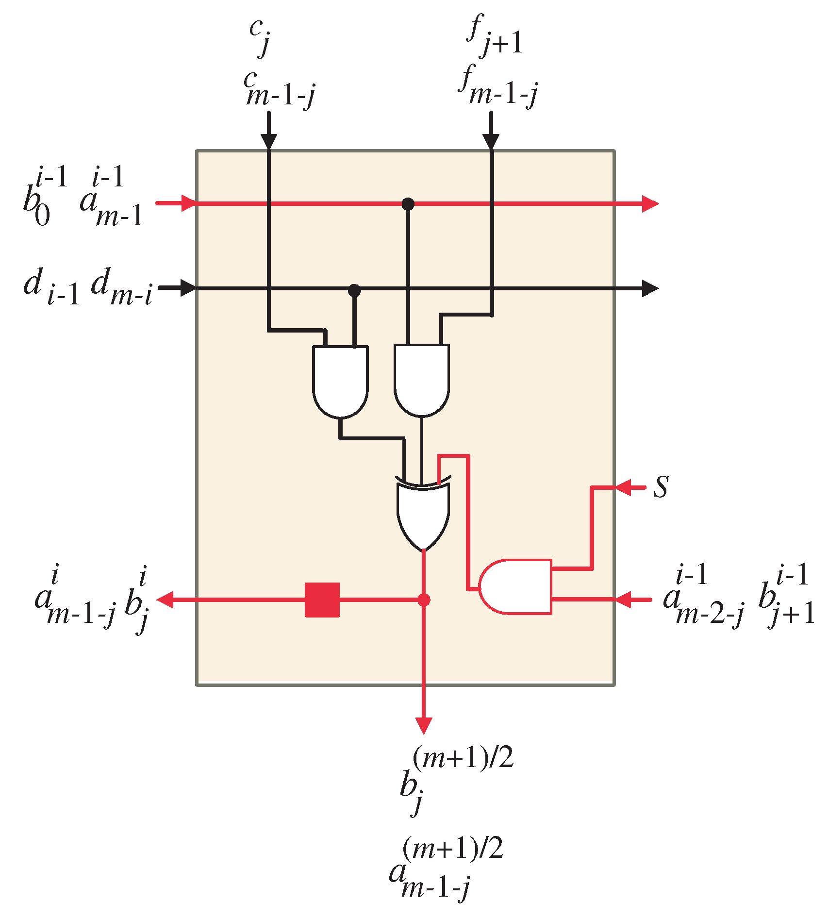
4.3. Semi-Systolic Multiplier Architecture

For each DG node or point, p [ i , j ] , we can acquire the G ( p ) and p ¯ ( p ) functions by including vectors s = [ 1 0 ] and H = [ 0 1 ] in Equations (12) and (18). The resultant functions can be defined as follows:
G ( p ) = i p ¯ ( p ) = j
By applying the derived functions of G ( p ) and p ¯ ( p ) to the DG points (nodes), we can extract the one-dimensional bit-parallel semi-systolic multiplier structure displayed in Figure 3. As depicted in Figure 3, the semi-systolic structure is composed of m regular PEs. The PEs’ internal logic is displayed in Figure 4. We can reduce the area and time complexities by modifying the PE logic by replacing the MUX component with an AND gate as shown in Figure 5. This modification will reduce the critical pass delay of the semi-systolic array to be represented as the summation of the delays of the 2-input AND gate and the 3-input XOR gate instead of 2-input MUX and 3-input XOR.
The proposed semi-systolic multiplier differs from the previously published two-dimensional parallel systolic designs in that it has an area complexity of order O ( m ) as opposed to O ( m 2 ) . Additionally, the semi-systolic array’s final output is accessible after a latency of ( m + 1 ) / 2 + 3 clock cycles, just like with the Montgomery two-dimensional parallel semi-systolic structures that have been recently published [32,33]. The resulting semi-systolic multiplier structure is superior to them in terms of space complexity. Moreover, the proposed multiplier structure outperforms the parallel multipliers that are based on the conventional field multiplication, [3,4,28,29,31,38,39], in terms of area and latency, as will be presented in the Results section.
By examining Figure 3 and Figure 4, we can describe the developed parallel semi-systolic multiplier’s layout as follows: The input signals c m 1 j , f m 1 j , c j , and f j + 1 are assigned to each PE. The initial values of input signals a m 2 j and b j + 1 , 0 j m 1 , are equal to zero. Therefore, the inputs at the right corners of the PEs are assigned zero values as shown in Figure 3. In addition, the initial values of input signals a m 1 and b 0 are equal to zero as indicated by the zero input shown on the left side of the semi-systolic array. The input signals d m i and d i 1 , 1 i ( m + 1 ) / 2 are fed in sequence and go through all the PEs. Each PE generates the intermediate signals of a m 1 j i and b j i , 1 i ( m + 1 ) / 2 and 0 j m 1 , in sequence and pipelined them through the D latch (the solid red box shown in Figure 4 and Figure 5) to the next PE. After ( m + 1 ) / 2 clock cycles, the resulting bits of a m 1 j ( m + 1 ) / 2 and b j ( m + 1 ) / 2 , 0 j m 1 will be available in parallel at the outputs of all the PEs. Signals of a m 1 j ( m + 1 ) / 2 are delayed by one clock cycle relative to signals of b j ( m + 1 ) / 2 , 0 j m 1 . This is implemented by using the latches (red boxes) shown at the output of the semi-systolic array shown in Figure 3. The final product bits p m 1 j , 0 j m 1 is obtained at clock cycle ( m + 1 ) / 2 + 3 from adding (using 2-input XOR gates) the bits of a m 1 j ( m + 1 ) / 2 and b j ( m + 1 ) / 2 , 0 j m 1 .
Following is an explanation of how the investigated bit-parallel semi-systolic multiplier structure functions:
  • Through the first two clock periods, select signal S is deactivated ( S = 0 ) to enforce the zero input bits of a m 2 j and b j + 1 , 0 j m 1 , to be localized in each PE. When S is equal to zero, the AND gate output will equal zero, which represents the initial values of a m 2 j and b j + 1 , 0 j m 1 . When S activates to one, the AND gate output will represent the intermediate values of the partial results of a m 2 j i 1 and b j + 1 i 1 , 0 j m 1 . At the same clock periods, the input bits of d m 1 and d 0 are fed in sequence to go through all the PEs.
  • The PEs produce the internal bit values a m 1 j i and b j i , 2 i ( m + 1 ) / 2 and 0 j m 1 , sequentially, over the forthcoming ( m + 1 ) / 2 1 clock periods. Additionally, all PEs receive input bits in a bit sequence from d m i and d i 1 , 2 i ( m + 1 ) / 2 .
  • The resultant output bits of the product P, p m 1 j , 0 j m 1 are produced in parallel at the outputs of XOR gates shown in Figure 3. They are generated at the last clock period ( m + 1 ) / 2 + 3 .

5. Results and Discussion

In this part, we compare the suggested one-dimensional bit-parallel semi-systolic multiplier to the previous impactful systolic/semi-systolic multiplier structures of [3,4,28,29,31,32,33,38,39] in addition to the competitive sequential multiplier of [34]. This section is divided into two subsections: The first one discusses in detail the area and time complexities of the proposed design and compares them to that of the competitive designs. The second subsection verifies the complexity analysis results using real implementation.

5.1. Complexity Analysis

As we notice from the offered semi-systolic structure depicted in Figure 3, it composed of regular m PEs having 3 m AND gates, m 3-input XOR gates that are equivalent to 2 m 2-input XOR gates, 0 MUXes, and 3 m Latches. Using m 2-input XOR gates, we added the resulting bits of a m 1 j ( m + 1 ) / 2 and b j ( m + 1 ) / 2 , 0 j m 1 , to produce the output bits of the final product p j . As a result, the overall number of used 2-input XOR gates ought to be 3 m . As was previously mentioned, the suggested multiplier takes ( m + 1 ) / 2 + 3 clock periods to generate the output results. By looking into the exact details of the PE logic, we can calculate the critical path delay (CPD) of the offered multiplier as the sum of the propagation delays of one 2-input AND gate ( T A ) and two 2-input XOR gates ( 2 T X ).
Table 1 estimates space in terms of the total number of utilized components (gates, MUXes, and latches), latency, and CPD of the recommended semi-systolic multiplier structure along with the currently available systolic/semi-systolic multiplier structures of [3,4,28,29,31,32,33,38,39] and the competitive sequential multiplier structure of [34]. Table 1 shows that the designs of [3,4,28,29,31,32,33,38] have an area complexity of order O ( m 2 ) , whereas the designs of [34,39], and the proposed one have an area complexity of order O ( m ) . In addition, it indicates that all the designs have time complexity of order O ( m ) . For IoT and embedded applications, the designs of [34,39] and the proposed one are more suitable than the other designs. Therefore, we will concentrate on comparing the proposed design to the competitive designs of [34,39]. In terms of area, we notice that the proposed design has m more AND and XOR gates than the competitive ones, but it has zero MUXes compared to them. In addition, the proposed design has the same latches compared to the design of [34] and the design of [39] has less area by m latches than the proposed one. On the other hand, the proposed design has significant less latency compared to the competitive designs of [34,39] and almost the same critical path delay (CPD). The real implementation results provided in Table 2 show that the proposed design has slightly lower area complexity and significantly lower time complexity than the competitive ones as we will discuss in the upcoming sections.

5.2. Implementation Results

To verify and assess the performance of the compared designs, we used VHDL programming language to model the recommended semi-systolic multiplier structure and the competing multiplier structures of [34,39]. The resultant code is synthesized by using Synopsis design compiler with Nangate library (1.5 nm, 0.8 V). The multiplier structures were tested using Modelsim’s functional verification tools before being synthesized. An evaluation of the power usage occurs at a frequency of 10 MHz.
For the recommended field sizes of m = 409 and m = 571 , we obtained the synthesis results of area, delay, and power consumption shown in Table 2. From the obtained synthesis results, we computed the design metrics of area–delay product (ADP) and power–delay product (PDP). Table 2 also illustrates the savings between the recommended bit-parallel semi-systolic multiplier structure and its competitors [34,39] in terms of space, consumed power, ADP, and PDP. The following can be seen by reading the results found in Table 2:
  • The suggested semi-systolic multiplier structure uses slightly less space and power than competing designs [34,39]. The average savings of area for m = 409 are ranging from 2% to 6.6% and ranging from 2.1% to 7.4% for m = 571 . The achievable average reduction in power consumptions for m = 409 of the developed multiplier structure over the competitive multiplier structures are ranging from 4.9% to 13.4% and ranging from 6.8% to 11.8% for m = 571 . The reduction in area and power is mainly due to the slightly lower gate counts and wire area of the proposed design over the competitive ones.
  • The suggested semi-systolic multiplier structure has significant savings in delay over the competitive designs of [34,39]. This is attributed to the significant reduction in latency of the proposed designs over the competitive ones. The average savings of delay for m = 409 are ranging from 49.2% to 50.0% and ranging from 45.9% to 46.4% for m = 571 ;
  • The ADP and PDP of the developed semi-systolic structure are significantly lower than those of the rival designs of [34,39]; The average reductions of ADP at m = 409 are ranging from 50.2% to 53.3% and ranging from 47.0% to 50.4% for m = 571 ; The achievable average reduction of PDP of the offered multiplier structure over the competitive ones for m = 409 is ranging from 51.7% to 56.7% and ranging from 49.5% to 52.8% for m = 571 .
As we notice from the acquired results, the suggested one-dimensional bit-parallel semi-systolic multiplier has marginal space and power savings. Additionally, it offers significant savings in terms of delay, ADP, and PDP results compared to the competitor ones. Therefore, the offered multiplier structure is more appropriate for use in devices with limited resources, such as IoT edge nodes and other tiny embedded devices.

6. Summary and Conclusions

In this article, we derived a low complexity one-dimensional bit-parallel semi-systolic array structure for polynomial-basis Montgomery multiplication in GF( 2 m ). A dependency graph can be used to depict the chosen algorithm, which is a standard iterative algorithm. We were able to acquire the feasible bit-parallel semi-systolic multiplier architecture by allocating the proper scheduling and node projection functions to each DG node. The developed one-dimensional parallel structure differs from the previously published two-dimensional parallel structures in that it has space complexity of order O ( m ) as opposed to order O ( m 2 ) of later ones. The recommended multiplier structure, like other systolic structures, has a modular structure with local connectivity between its PEs. This feature makes the recommended multiplier design more appropriate for VLSI implementation. According to the space and time complexities analysis, the offered multiplier has a significant reduction in delay when compared to the majority of the parallel competitive multipliers, as well as a comparable number of logic components. To confirm the findings of the complexity analysis, we used the ASIC CMOS library to synthesize the suggested and the previously described one-dimensional multiplier architectures to assess their performance. According to the acquired results, the offered multiplier architecture has marginal space and power savings compared to the competitive multiplier structures. In addition, it has significant savings in delay, area–delay, and power–delay products. Therefore, we can conclude that the offered multiplier architecture is appropriate for use in devices with limited resources, such as IoT edge nodes and tiny embedded systems. We will merge the recommended multiplier architecture into the ECC crypto-processor in the forthcoming project to quantify the system’s overall space, time, and energy savings.

Author Contributions

Conceptualization, A.I.; methodology, A.I. and F.G.; software, A.I.; validation, U.T.; formal analysis, A.I.; investigation, A.I.; resources, A.I. and T.A.A.; data curation, A.I.; writing—original draft preparation, A.I.; writing—review and editing, A.I. and F.G.; visualization, A.I. and U.T.; supervision, A.I.; project administration, A.I. and F.G.; funding acquisition, A.I. and F.G. All authors have read and agreed to the published version of the manuscript.

Funding

Deputyship for Research & Innovation, Ministry of Education in Saudi Arabia, project number (IF2-PSAU-2022/01/21637).

Institutional Review Board Statement

Not applicable.

Informed Consent Statement

Not applicable.

Data Availability Statement

Not applicable.

Acknowledgments

The authors extend their appreciation to the Deputyship for Research & Innovation, Ministry of Education in Saudi Arabia for funding this research work through the project number (IF2-PSAU-2022/01/21637).

Conflicts of Interest

The authors declare no conflict of interest.

Abbreviations

The following abbreviations are used in this manuscript:
IoTInternet of Things
ADPArea–Delay Product
PDPPower–Delay Product
ASICApplication Specific Integrated Circuit
ECCElliptic Curve Cryptography
DGDependency Graph
CPDCritical Path Delay

References

  1. Chen, C.C.; Lee, C.Y.; Lu, E.H. Scalable and Systolic Montgomery Multipliers Over GF(2m). IEICE Trans. Fundam. 2008, E91-A, 1763–1771. [Google Scholar] [CrossRef]
  2. Chiou, C.W.; Lee, C.Y.; Deng, A.W.; Lin, J.M. Concurrent error detection in Montgomery multiplication over GF(2m). IEICE Trans. Fundam. Electron. Commun. Comput. Sci. 2006, E89-A, 566–574. [Google Scholar] [CrossRef]
  3. Huang, W.T.; Chang, C.; Chiou, C.; Chou, F. Concurrent error detection and correction in a polynomial basis multiplier over GF(2m). IET Inf. Secur. 2010, 4, 111–124. [Google Scholar] [CrossRef]
  4. Kim, K.W.; Jeon, J.C. Polynomial Basis Multiplier Using Cellular Systolic Architecture. IETE J. Res. 2014, 60, 194–199. [Google Scholar] [CrossRef]
  5. Choi, S.; Lee, K. Efficient systolic modular multiplier/squarer for fast exponentiation over GF(2m). IEICE Electron. Express 2015, 12, 1–6. [Google Scholar] [CrossRef] [Green Version]
  6. Reyhani-Masoleh, A. A new bit-serial architecture for field multiplication using polynomial bases. In Cryptographic Hardware and Embedded Systems, Proceedings of the 7th International Workshop Cryptographic Hardware Embedded Systems (CHES 2008), Washington, DC, USA, 10–13 August 2008; Springer: Berlin/Heidelberg, Germany, 2008; pp. 314–330. [Google Scholar]
  7. Abdulrahman, E.A.; Reyhani-Masoleh, A. High-Speed Hybrid-Double Multiplication Architectures Using New Serial-Out Bit-Level Mastrovito Multipliers. IEEE Trans. Comput. 2016, 65, 1734–1747. [Google Scholar] [CrossRef]
  8. Kim, K.W.; Jeon, J.C. A semi-systolic Montgomery multiplier over GF(2m). IEICE Electron. Express 2015, 12, 20150769. [Google Scholar] [CrossRef] [Green Version]
  9. Ibrahim, A. Novel Bit-Serial Semi-Systolic Array Structure for Simultaneously Computing Field Multiplication and Squaring. IEICE Electron. Express 2019, 16, 20190600. [Google Scholar] [CrossRef] [Green Version]
  10. Kim, K.W.; Lee, J.D. Efficient unified semi-systolic arrays for multiplication and squaring over GF(2m). Electron. Express 2017, 14, 20170458. [Google Scholar] [CrossRef] [Green Version]
  11. Kim, K.W.; Kim, S.H. Efficient bit-parallel systolic architecture for multiplication and squaring over GF(2m). IEICE Electron. Express 2018, 15, 20171195. [Google Scholar] [CrossRef]
  12. Ibrahim, A. Efficient Parallel and Serial Systolic Structures for Multiplication and Squaring Over GF(2m). Can. J. Electr. Comput. Eng. 2019, 42, 114–120. [Google Scholar] [CrossRef]
  13. Roman, S. Field Theory, 2nd ed.; Springer: New York, NY, USA, 1983. [Google Scholar]
  14. Pillutla, S.R.; Boppana, L. Area-efficient low-latency polynomial basis finite field GF(2m) systolic multiplier for a class of trinomials. Microelectron. J. 2020, 97, 104709. [Google Scholar] [CrossRef]
  15. Imana, J.L. LFSR-Based Bit-Serial GF(2m) Multipliers Using Irreducible Trinomials. IEEE Trans. Comput. 2020, 70, 156–162. [Google Scholar]
  16. Pillutla, S.R.; Boppana, L. Low-latency area-efficient systolic bit-parallel GF(2m) multiplier for a narrow class of trinomials. Microelectron. J. 2021, 117, 105275. [Google Scholar] [CrossRef]
  17. Li, Y.; Cui, X.; Zhang, Y. An Efficient CRT-based Bit-parallel Multiplier for Special Pentanomials. IEEE Trans. Comput. 2021, 71, 736–742. [Google Scholar] [CrossRef]
  18. Li, Y.; Zhang, Y.; He, W. Fast hybrid Karatsuba multiplier for type II pentanomials. IEEE Trans. Very Large Scale Integr. (Vlsi) Syst. 2020, 28, 2459–2463. [Google Scholar] [CrossRef]
  19. Meher, P.K.; Lou, X. Low-Latency, Low-Area, and Scalable Systolic-Like Modular Multipliers for GF(2m) Based on Irreducible All-One Polynomials. IEEE Trans. Circuits Syst. Regul. Pap. 2016, 64, 399–408. [Google Scholar] [CrossRef]
  20. Mohaghegh, S.; Yemiscoglu, G.; Muhtaroglu, A. Low-Power and Area-Efficient Finite Field Multiplier Architecture Based on Irreducible All-One Polynomials. In Proceedings of the 2020 IEEE International Symposium on Circuits and Systems (ISCAS), Seville, Spain, 12–14 October 2020; pp. 1–5. [Google Scholar]
  21. Zhang, Y.; Li, Y. Efficient Hybrid GF(2m) Multiplier for All-One Polynomial Using Varied Karatsuba Algorithm. IEICE Trans. Fundam. Electron. Comput. Sci. 2021, 104, 636–639. [Google Scholar] [CrossRef]
  22. Zhou, B.B. A New Bit Serial Systolic Multiplier over GF(2m). IEEE Trans. Comput. 1988, 37, 749–751. [Google Scholar] [CrossRef]
  23. Fenn, S.T.J.; Taylor, D.; Benaissa, M. A Dual Basis Bit Serial Systolic Multiplier for GF(2m). Integration 1995, 18, 139–149. [Google Scholar] [CrossRef]
  24. Lee, C.Y.; Lu, E.H.; Lee, J.Y. Bit-Parallel Systolic Multipliers for GF(2m) Fields Defined by All-One and Equally-Spaced Polynomials. IEEE Trans. Comput. 2001, 50, 358–393. [Google Scholar]
  25. Lee, C.Y.; Lu, E.H.; Sun, L.F. Low-Complexity Bit-Parallel Systolic Architecture for Computing AB2+C in a Class of Finite Field GF(2m). IEEE Trans. Circuits Syst. II 2001, 50, 519–523. [Google Scholar]
  26. Lee, C.Y.; Chiou, C.W. Efficient Design of Low-Complexity Bit-Parallel Systolic Hankel Multipliers to Implement Multiplication in Normal and Dual Bases of GF(2m). IEICE Trans. Fundam. Electron. Commun. Comput. Sci. 2005, E88-A, 3169–3179. [Google Scholar] [CrossRef]
  27. Lee, C.Y. Low-latency bit-pararallel systolic multiplier for irreducible xm+xn+1 with GCD(m,n)=1. IEICE Trans. Fund. Elect. Commun. Comput. Sci. 2008, 55, 828–837. [Google Scholar]
  28. Bayat-Sarmadi, S.; Farmani, M. High-Throughput Low-Complexity Systolic Montgomery Multiplication Over GF(2m) Based on Trinomials. IEEE Trans. Circuits Syst. II 2015, 62, 377–381. [Google Scholar] [CrossRef]
  29. Mathe, S.E.; Boppana, L. Bit-parallel systolic multiplier over GF(2m) for irreducible trinomials with ASIC and FPGA implementations. IET Circuits Desvices Syst. 2018, 12, 315–325. [Google Scholar] [CrossRef]
  30. Lee, C.Y.; Chiou, C.W.; Lin, J.M. Concurrent error detection in a polynomial basis multiplier over GF(2m). J. Electron. Test. 2006, 22, 143–150. [Google Scholar] [CrossRef]
  31. Chiou, C.W.; Lee, C.M.; Sun, Y.S.; Lee, C.Y.; Lin, J.M. High-throughput Dickson basis multiplier with a trinomial for lightweight cryptosystems. IET Comput. Digit. Tech. 2018, 12, 187–191. [Google Scholar] [CrossRef]
  32. Lee, K. Resource and Delay Efficient Polynomial Multiplier over Finite Fields GF(2m). J. Korea Soc. Digit. Ind. Inf. Manag. 2020, 16, 1–9. [Google Scholar]
  33. Lee, K. Low Complexity Systolic Montgomery Multiplication over Finite Fields GF(2m). J. Korea Soc. Digit. Ind. Inf. Manag. 2022, 18, 1–9. [Google Scholar]
  34. Mathe, S.E.; Boppana, L. Design and Implementation of a Sequential Polynomial Basis Multiplier over GF(2m). KSII Trans. Int. Inf. Syst. 2017, 11, 2680–2700. [Google Scholar]
  35. Gebali, F. Algorithms and Parallel Computers; John Wiley: New York, NY, USA, 2011. [Google Scholar]
  36. Ibrahim, A.; Gebali, F. Scalable and Unified Digit-Serial Processor Array Architecture for Multiplication and Inversion over GF(2m). IEEE Trans. Circuits Syst. I Regul. Pap. 2017, 22, 2894–2906. [Google Scholar] [CrossRef]
  37. Ibrahim, A.; Alsomani, T.; Gebali, F. New Systolic Array Architecture for Finite Field Inversion. IEEE Can. J. Electr. Comput. Eng. 2017, 40, 23–30. [Google Scholar] [CrossRef]
  38. Chiou, C.W.; Lin, J.M.; Lee, C.Y.; Ma, C.T. Novel Mastrovito Multiplier over GF(2m) Using Trinomial. In Proceedings of the 2011 5th International Conference on Genetic and Evolutionary Computing (ICGEC), Kitakyushu, Japan, 29 August–1 September 2011; pp. 237–242. [Google Scholar]
  39. Ibrahim, A.; Gebali, F.; Bouteraa, Y.; Tariq, U.; Ahanger, T.; Alnowaiser, K. Compact Bit-Parallel Systolic Multiplier Over GF(2m). IEEE Can. J. Electr. Comput. Eng. 2021, 44, 199–205. [Google Scholar] [CrossRef]
Figure 1. DG of the Montgomery algorithm for m = 5 .
Mathematics 11 00111 g001
Figure 2. Node timing for m = 5 .
Mathematics 11 00111 g002
Figure 3. Semi-systolic bit-parallel multiplier structure.
Mathematics 11 00111 g003
Figure 4. Logic diagram of PE j .
Mathematics 11 00111 g004
Figure 5. Simplified Logic diagram of PE j .
Mathematics 11 00111 g005
Table 1. Complexity analyses in terms of area and time of the suggested and the existing multipliers.
DesignANDXORMUXLatchLatencyCPDArea ComplexityTime Complexity
Huang [3] 2 m 2 2 m 2 0 2 m 2 + m + 1 m + 1 T A + T X O ( m 2 ) O ( m )
Chiou [31] m 2 3 m 2 + 2 m 0 3 m 2 + 4 m m + 1 T A + 3 T X O ( m 2 ) O ( m )
Lee [32] m 2 + m m 2 + 2 m 0 1.6 m 2 + 4 m ( m + 7 ) / 2 T A + T X O ( m 2 ) O ( m )
Lee [33] m 2 + m m 2 + ( 7 m + 1 ) / 2 0 2.1 m 2 + 6.5 m ( m + 7 ) / 2 T A + T X O ( m 2 ) O ( m )
Chiou [38] m 2 m 2 + m m 2 m 2 + 3 m m + 1 T A + T X + T M O ( m 2 ) O ( m )
Kim [4] 2 m 2 + 2 m 2 m 2 + 3 m 0 3 m 2 + 4 m m 2 + 1 T A + T X O ( m 2 ) O ( m )
Sarmadi [28]( m 2 ) * 1.5 m 2 + 0.5 m 1.5 m 2 2.5 m + 3 1.5 m 2 + 2 m 1 m + 2 T N + T X O ( m 2 ) O ( m )
Mathe [29]m m 2 1 m 2 m m 2 m T M + 2 T X O ( m 2 ) O ( m )
Mathe [34] 2 m 2 m 2 m 3 m m T A + T X + T M O ( m ) O ( m )
Ibrahim [39] 2 m 2 m 3 m 2 m m T A + T X + T M O ( m ) O ( m )
Proposed 3 m 3 m 0 3 m ( m + 7 ) / 2 T A + 2 T X O ( m ) O ( m )
(∗) 2-input NAND gates.
Table 2. Analyzing the performance of different multiplier structures for the values of m = 409 and m = 571 .
MultiplierTypemArea
[Kgates]
Delay
[ns]
Power
[mW]
ADPPDPArea Saving
(%)
Delay Saving
(%)
Power Saving
(%)
ADP Saving
(%)
PDP Saving
(%)
Mathe [34]Sequential40910.613.46.7142.089.86.650.013.453.356.7
57114.918.39.3272.7170.27.446.411.850.452.8
Ibrahim [39]Systolic40910.113.26.1133.380.52.049.24.950.251.7
57114.118.18.8255.2159.32.145.96.847.049.5
ProposedSystolic4099.96.75.866.338.9----
57113.89.88.2135.280.4----
Disclaimer/Publisher’s Note: The statements, opinions and data contained in all publications are solely those of the individual author(s) and contributor(s) and not of MDPI and/or the editor(s). MDPI and/or the editor(s) disclaim responsibility for any injury to people or property resulting from any ideas, methods, instructions or products referred to in the content.

