1. Introduction
In recent years, the use of mobile devices with short battery life has expanded significantly. Wearable technology, mobile phones, tablet computers, and handheld devices are examples of a few of those devices. Power consumption and delay are the major issues arising due to the short battery life of these devices [
1,
2]. Many applications of image processing are fault tolerant. The approximation has recently become a viable option for reducing circuit factors [
3]. Hardware constraints can be solved via circuit design to some extent, however, it will entail sacrificing precision. Full Adder circuits play the primary role in many mathematical systems. These can be used in multipliers, adders, subtractors and more complex structures [
4,
5]. Therefore, building a high-performance Full Adder cell is essential.
By 2006, MOSFET transistors had reached a nanoscale dimension of 65 nm [
6]. In the Nano region, bulk silicon MOSFETs commonly suffer from high parametric variations and increased leakage currents [
7]. There have been numerous advances in post-silicon technologies designed to overcome the problems associated with nanoscale MOSFETs. A CNFET device has remarkable electrical properties. Since they conduct charge carriers near ballistic conduction and have low off-currents, they are inherently fast and low-powered [
8]. These features make CNFETs a promising alternative to its competitors. Thin graphite tubes are called CNTs. It is formed by spinning graphite composed of hexagonal carbon, called graphene, into CNTs [
9]. A CNT can be either metallic or semiconductor based on its chirality vector.
In this paper, we propose a new design of a 1-bit Full Adder. For assessment, the presented Adder is compared to several progressive inaccurate Adders. We also simulate changes in voltage, output load, and temperature using software simulations. Based on the simulation results, the proposed cell performs better in delay, PDP, and EDP. Following that, the proposed inaccurate Adder is used in alpha blending applications. PSNR and SSIM are used to assess the efficiency of inaccurate circuits. Two merit figures are used to reconcile transistor results with application results.
In
Section 2, we discourse the primary concepts of CNFET and inaccurate computing.
Section 3 investigates the pros and cons of several advanced inaccurate Full Adders. In
Section 4 and
Section 5, we present the detailed design and simulation results, respectively, and in
Section 6, the article is summarized and future works are introduced.
2. Literature Review
As a method of increasing hardware metrics, such as energy consumption, delay and area, approximate computation is a computationally efficient solution [
3,
10]. We examine some of the main error metrics in Equations (1) and (2). It should be noted that the symbols S, S’, and N indicate the accurate output, inaccurate output and the number of input signals, respectively. The first characteristic is the error distance. It refers to the absolute difference between inaccurate and accurate results [
11,
12].
In the design of high-performance circuits, it is important to minimize the length of the critical path. The critical path is defined as the longest temporal path from the circuit input to its output.
Several advanced inaccurate Full Adder circuits are discussed in detail based on their transistor level and accuracy.
In [
13], a bridge-based inexact Full Adder is proposed. This circuit has twelve transistors. Both outputs of this design are full-swing. The Cout output is derived from the SUM output, and it becomes weak while driving large loads. The weak SUM signal results in slower Cout switching speeds. Consequently, this design has a considerable delay. Due to the precision of the Cout output, the calculation error in one level does not propagate to the next levels with higher significance values. Out of the eight possible input combinations, two of the SUM signals are incorrect.
Two Full Adder circuits proposed in [
14] have thirteen and nine transistors (13T, 9T), respectively. In this design, the circuits are based on the Capacitive Threshold Logic (CTL) technique. The first design comprises thirteen transistors, four of which are located on the critical path. Inverters at the outputs ensure that the Cout and SUM have a full voltage swing. There are only nine transistors in the second scheme, three of which are located on the critical path. The SUM output in the second scheme is not derived by a strong signal. It is worth mentioning that both schemes have high energy consumption due to using a capacitor network with three inputs to generate non-full swing signals. In both schemes, there are three incorrect combinations in the SUM output, while the Cout output is never incorrect. As a result, these designs are less accurate than those described in [
13].
Eight transistors are in the circuit [
15]. Both outputs are full-swing. The SUM output derives the Cout output, as in the scheme [
13]. The SUM signal becomes weak when it drives large loads. The Cout output switches slower when the SUM signal is weak. As a result, this circuit is expected to have a long delay. In scheme [
16], both output signals are inaccurate. Using the Cout signal, the error is transferred to the higher significant bits.
There are nine transistors in a CMOS style scheme in the circuit [
17]. The drawback of this design emerges because the Cout signal depends on the SUM signal. As a result, large loads significantly increase power and delay. In this circuit, both Cout and SUM signals are produced with incorrect values. Consequently, errors are transferred to higher significant bit positions as in [
15].
There are fifteen transistors in the scheme [
18], four of which are located along the critical path. To generate internal signals, it uses two capacitor networks. The output of the capacitive network section is a non-full voltage swing, which increases the energy consumption. Three inverters are devised at the output section to produce the high drive capacity. This circuit’s SUM signal values are incorrect, but Cout signals remain correct.
There are eight transistors in the inexact circuit in [
19], four of which are located on the critical path. Unlike Cout, the SUM signal is full-swing in this circuit. The Cout output derives the SUM output. As a result, the Cout signal becomes weak while driving large loads.
In [
20], a new exact Full Adder is proposed. This design has ten transistors and it suffers from threshold loss on both outputs. Therefore, it is unable to carry large loads effectively.
To conclude,
Table 1 summarizes some of the criteria of the various Full Adder designs in terms of transistor level and accuracy.
3. Proposed Method
Table 2 presents the approximate design and the truth table of the suggested Full Adder. The Cout and SUM outputs produce one and three incorrect values, respectively.
To develop an efficient approximate Full Adder, a balance must be achieved between the logic and transistor levels. This necessitates tolerable imprecision in the logic circuit to allow for an acceptable error margin at the application level, such as in image processing. Meanwhile, the transistor-level considerations must prioritize low delay and power consumption characteristics. Consequently, the design process entails concurrent completion of the truth table and the transistor-level circuit.
In addition, the truth table of the proposed design should be simplified relative to the truth table of the exact Full Adder circuit. This simplification makes the final circuit require a smaller number of transistors for implementation. However, it is of utmost importance to maintain a minimal increase in the error distance, as a significant increase in the error distance will lead to a decrease in the efficiency of the circuit at the application level. Moreover, the design process necessitates careful consideration of the trade-off between achieving a full-swing design and minimizing transistor usage. Neglecting both these aspects would lead to heightened power consumption and delay.
Equations (3) and (4) generate the SUM and Cout outputs, respectively. To achieve maximum symmetry in the design, a combination of an OR gate and two 2:1 multiplexers (MUXs) was employed, with the OR gate serving as a data selector for the MUXs. Therefore, the presented design benefits from a symmetrical architecture [
21].
Figure 1 shows the architecture of the presented Full Adder cell at the transistor level. To implement a NOR gate with two inputs, a CMOS-style scheme is used. Then, an OR function is generated using a simple inverter. All internal nodes are of full-swing design. Therefore, lower energy consumption and more excellent drive capability are expected. With a rail-to-rail signal in the output, the presented cell ensures appropriate performance when there are large loads [
22]. The proposed cell contains fourteen transistors, four of which are located on its critical path.
The presented scheme produces independent SUM and Cout output signals. Therefore, the proposed cell’s output signals can drive large loads properly. A CNFET device with three tubes as transistor channels simulates the proposed cell.
4. Hardware-Level Simulation Results
Hardware-level simulations are performed via the HSPICE software (H-2013.03) using Circuit-Compatible SPICE 32 nm CNFET model [
16,
23].
Table 3 presents a tabulated representation of the significant parameters encompassed within this model.
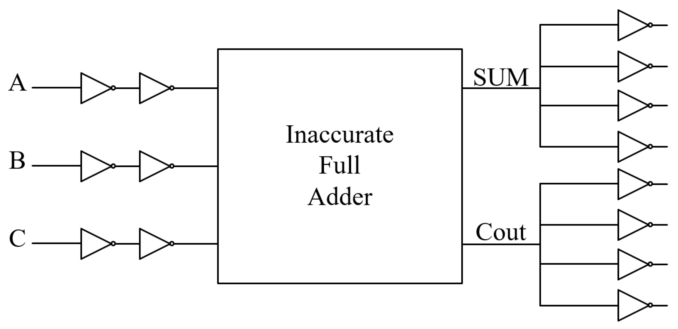
Figure 2 shows the simulation testbed [
24]. In order to examine the performance of the approximate Full Adders, we apply a comprehensive test pattern that incorporates all possible input transitions. Circuit delay is calculated by considering all transmissions at the outputs and reporting the maximum amount. Moreover, the average energy consumption is calculated. PDP and EDP criteria are also considered [
25,
26].
Simulated circuits are tested in the range of 0.8 V to 1 V VDD at 25 °C and 1 GHz at FO4 load to evaluate performance against different power supplies.
Table 4 shows the simulation results. The results indicate that the presented Full Adder performs better than its competitors. Additionally, to unify the simulation conditions, all CNTs in the presented circuit and competitor circuits have a diameter of 1.4877 nm. To assess the circuit parameters comprehensively, a duration of 32.5 s has been selected as the period for conducting an exhaustive test.
Upon examination of
Table 4, it can be concluded that the suggested cell exhibits superior performance in regard to delay, PDP and EDP metrics across all supply voltages in comparison to its counterparts. As an illustrative example, at 1 V VDD, the suggested cell has 49%, 29%, 19%, 31%, 42%, 17%, 18% and 19% less delay and 52%, 81%, 79%, 24%, 37%, 79%, 7% and 35% less PDP in comparison to [
13], [
14] (13T), [
14] (9T), [
15], [
17], [
18], [
19] and [
20], respectively.
It is crucial to examine the circuit performance under varying output loads. All circuits are simulated at 0.9 V VDD, 25 °C, and 1 GHz frequency against various output loads. The simulation results are shown in
Figure 3. The suggested cell demonstrates successful performance under variation of loads, in contrast to other cells which exhibit inadequacy in handling large loads. Based on the simulation results, it is clear that the presented Full Adder has the best delay, PDP and EDP for various loads. As expected, circuits with non-full swing nodes perform unacceptably against large loads.
As an illustrative example, at FO8, the suggested cell has 60%, 18%, 10%, 42%, 48%, 5%, 27% and 39% less delay and 61%, 52%, 48%, 32%, 41%, 50%, 45% and 16% less PDP in comparison to [
13], [
14] (13T), [
14] (9T), [
15], [
17], [
18], [
19] and [
20], respectively.
In circuit evaluation, temperature resistance is one of the most important criteria.
Figure 4 shows the performance of the designs at different temperatures. As expected, circuits that include capacitor networks perform unacceptably against high temperatures.
The proposed cell appears to function properly and to be resistant to temperature changes, as shown in
Figure 4. PDP and EDP of the presented Full Adder remain almost constant without any significant changes.
The performance of all circuits is investigated over a range of clock frequencies at 0.9 V power supply, 25 °C temperature, and FO4. The simulation results are shown in
Figure 5. Clearly, the presented Full Adder has the best delay, PDP and EDP among its peers at all frequencies.
5. Application of Presented Full Adder
Alpha blending (image blending) systems are among the most popular image processing applications [
27]. The process of alpha blending involves the overlay of a transparent foreground image onto a background image. This process is shown in
Figure 6. This technique is commonly utilized in the domain of computer graphics and image editing.
Alpha blending can be achieved by combining two pictures, as shown in Equation (5).
where, α is the alpha ratio and serves as a determinant for the degree of image manifestation and lies within the range [0, 1]. Furthermore, P1 and P2 are input pictures [
28].
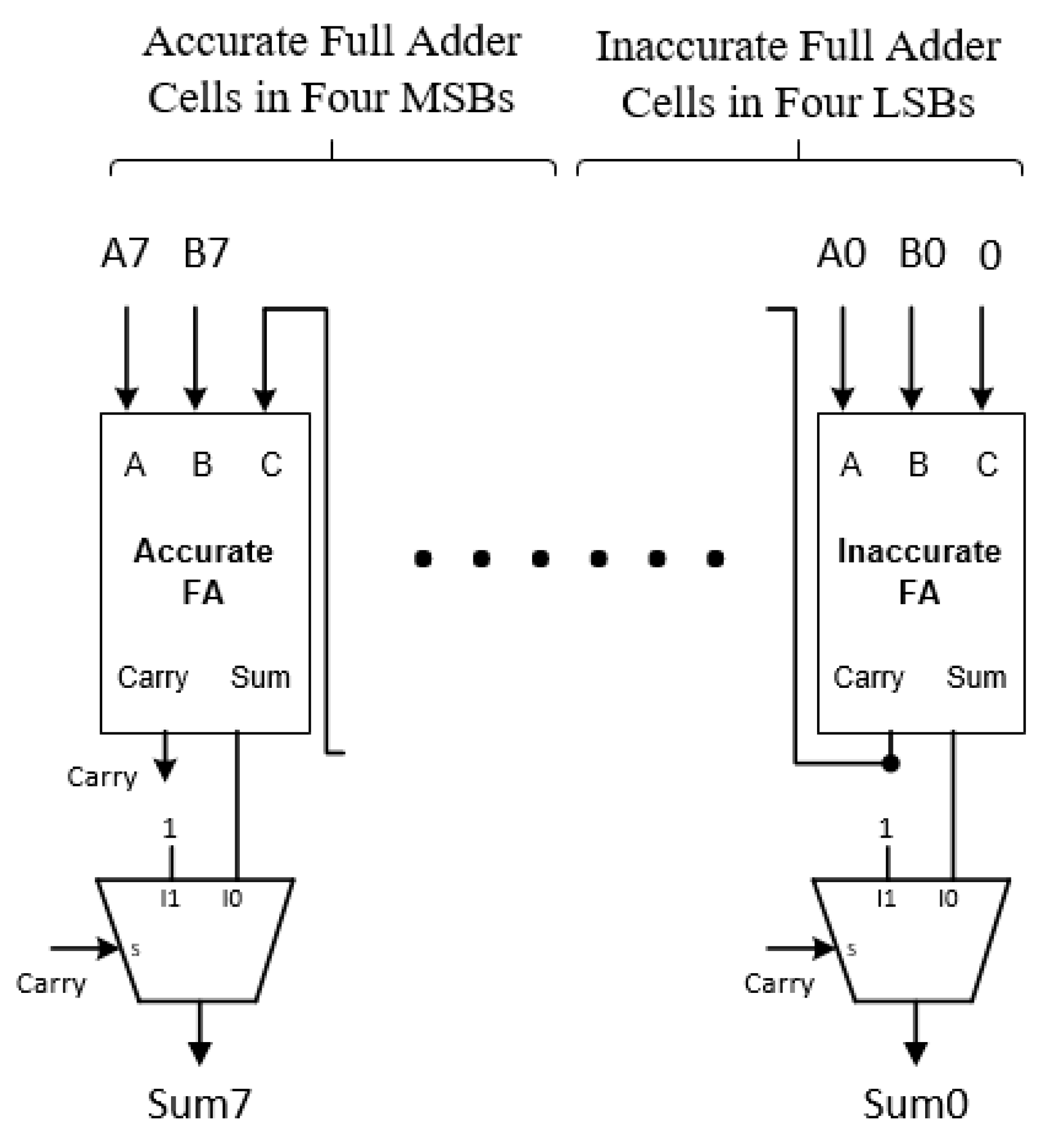
Alpha blending for a wide range of α has been performed using MATLAB [
29,
30]. The architecture of accurate and inaccurate Full Adder cells is presented in
Figure 7. Indeed, this 8-bit Full Adder is positioned within the adder block, as depicted in
Figure 6.
The results of the Alpha blending of images for α = 0.5 are shown in
Figure 8. As seen from the results, the inaccurate images possess acceptable quality against the main pictures.
PSNR is a commendable characteristic for evaluating image quality [
31]. SSIM is the structural similarity index measure and quantifies the similarity between the reference and the target pictures [
32]. Evidently, high PSNR and SSIM quantities are preferred. Moreover, two characteristics are used to create a reconciliation with different design levels. Equations (6) and (7) define the merit criteria. A lower FOM value indicates better results [
29].
Table 5 presents the simulation results obtained according to the presented architecture in
Figure 7 for α = 0.2, 0.5 and 0.8. All circuits are simulated at 0.9 V VDD, 25 °C, and 1 GHz frequency.
Simulations indicate that the presented design closely competes with its peers in respect of PSNR and SSIM, and also has the best FOMs.
The superiority of the proposed circuit in the FOMs characteristic confirms that it has the best performance among its competitors in terms of compromising the application level and circuit characteristics.
6. Conclusions
This paper proposes an advanced Full Adder cell that accepts errors in numerical outputs. We investigated the performance of the designs through extensive computer simulations. HSPICE was used to examine the efficiency of circuits under various VDDs, Fan-outs, working temperatures, and frequencies. In addition, MATLAB software (H-2013.03) was used to evaluate circuit performance at the application level.
Simulations demonstrate that the presented design is superior in transistor and application levels compared to its competitors.
Significant reduction in delay and as a result EDP and PDP while maintaining output accuracy compared to competitors are the main advantages of this circuit. The adoption of the proposed design for an inexact Full Adder cell yields a notable decrease of 12%, 7%, and 23% in the metrics of delay, PDP and EDP, respectively.
On the other hand, the presence of more transistors than its competitors which increases the consumption area and to some extent the power consumption are the main disadvantages of this design.
In consideration of further work, the designing of inexact compressors and multipliers employing the cell presented in this study will be subject to scrutiny. Moreover, the dynamic calibration of the precision of the Full Adder cells is subjected for future investigation.


