Article

Anti-Disturbance Bumpless Transfer Control for a Switched Systems via a Switched Equivalent-Input-Disturbance Approach

1
School of Information Science and Technology, Beijing University of Technology, Beijing 100124, China
2
Beijing Institute of Artificial Intelligence, and School of Information Science and Technology, Beijing University of Technology, Beijing 100124, China
*
Author to whom correspondence should be addressed.
Mathematics 2024, 12(15), 2307; https://doi.org/10.3390/math12152307
Submission received: 13 June 2024 / Revised: 19 July 2024 / Accepted: 19 July 2024 / Published: 23 July 2024
(This article belongs to the Special Issue Complex Process Modeling and Control Based on AI Technology)

Abstract

:
This paper concentrates on the issue of anti-disturbance bumpless transfer (ADBT) control design for switched systems. The ADBT control design problem refers to designing a continuous controller and a switching rule to ensure the switched system satisfies the ADBT property. First, the concept of the ADBT property is introduced. Then, via a switched equivalent-input-disturbance (EID) methodology, a switched EID estimator is formulated to estimate the impact of external disturbances within the switched system. Second, a bumpless transfer control is then constructed via a compensator integrating an EID estimation. Finally, the effectiveness of the presented control scheme is verified by controlling a switching resistor–inductor–capacitor circuit on the Matlab platform. Above all, a new configuration for ADBT control of switched systems is established via a switched EID methodology.

1. Introduction

With the advancement in control technologies, switching control is extensively utilized across engineering practices to meet various control requirements [1,2]. However, the sudden change in the control input signal during switching can occasionally adversely affect the dynamic behaviour of a practical system [3,4]. Meanwhile, external and internal disturbances are unavoidable during the operation of automated systems, which can potentially cause decreased efficiency or even instability [5,6]. Thereby, the ADBT control technique is significant for effectively suppressing disturbances, ensuring smooth transitions during control system switching, and guaranteeing stable system operation.
Anti-disturbance (AD) control techniques effectively attenuate unpredictable disturbances [7,8,9]. Many existing AD control methods have been proposed so far to achieve efficient disturbance suppression, such as output regulation theory [10,11], adaptive robust control theory [12,13] and active disturbance rejection control [14,15,16]. The EID approach, as an effectively active disturbance rejection method, is introduced to counteract both anticipated and unanticipated disruptions [17,18]. Utilizing a signal within the channel of the control input, this approach creates an equivalent effect on the output which is induced by actual disturbances. However, most of the existing results via the EID approach are for nonswitched systems, and these results cannot be applied to switched systems directly. In fact, differing from nonswitched systems, the EID estimator design and AD analysis for switched systems possess greater complexity and difficulty.
For switched systems, transient behaviours are inevitable when switching between different subsystems [19,20,21]. At the switching instant, the control input signal undergoes abrupt changes, which often results in undesirable transient performance between different controllers. BT control effectively mitigates bumps during switching transitions. Recently, based on different definitions of the BT level, many controller designing strategies are introduced to guarantee the BT performance for switched systems, such as event-triggered controller designs [22,23], state-dependent switching methods [24,25], time-dependent switching methods [26,27] and compensation-based BT controllers [28,29]. The concept of compensation is often employed to address the BT problem [29]. Yan Shi et al. introduce a straightforward bumpless transfer control framework that includes components such as a differentiator and an integrator for maintaining the smoothness of control [29]. Additionally, a compensator is implemented to address deviations from the original switching control input signal, aiming to eliminate steady-state errors. Further, it is essential to preserve switching transient performance when handling both matched and unmatched disturbances.
In this work, a switching methodology based on average dwell time (ADT) and a switched EID estimator are presented for the control of switched linear systems to suppress unknown disturbances via ADBT control. To summarize, the following contributions are proposed:
  • Although there exist many works on the ADBT control design problem, such as [10,30,31], the definitions of the ADBT control problem are different. In all these works, the BT performance is described by limiting the jump amplitude at switching instants or the amplitude difference between the actual control law u ( t ) and the auxiliary control signal v ( t ) rather than requiring the controller to operate continuously. In our work, a continuous controller is obtained. Moreover, in these existing works, H reliable controller design (as in [30]) and disturbance observer design (as in [10,31]) are always provided to achieve the AD performance. However, a switched EID methodology is introduced in our paper to achieve the AD performance. In fact, rare results are provided on the design of the switched EID estimator for switched systems.
  • We extend the EID estimator design issue from its original nonswitched version. The switched EID estimator, which relies on switching signals, indicates that each subsystem possesses its own EID estimator. To reduce the conservativeness that arises from using a common EID estimator for all subsystems, distinct EID estimators are designed for each subsystem.
  • Based on the switched EID estimator, through the construction of an additional compensator, a new formulation for the ADBT controller is devised for switched systems. Through an ADT switching methodology, sufficient conditions are derived for the ADBT control of switched systems. A continuous controller and an ADT switching strategy are jointly developed to address the ADBT control design problem for switched systems.
Below, we outline the organization of our work. It begins with the configuration of switched EID-based ADBT control and problem formulation in Section 2. The ADBT control designing analysis is put forward in Section 3. The effectiveness is demonstrated using a model of a switching RLC circuit, discussed in Section 4. A discussion is provided in Section 5. Lastly, our study is concluded in Section 6.
NotationsMeaning
R n n-dimensional real vector space
x 2-norm of x
λ m a x ( P ) ( λ m i n ( P ) )Greatest (least) eigenvalue of the matrix P
NSet of natural numbers
LMILinear matrix inequality

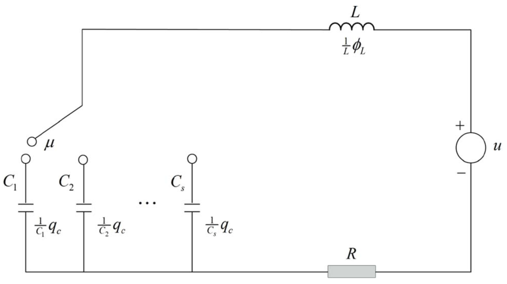
2. Configuration of Switched EID-Based ADBT Control and Problem Formulation

Take into account a switched linear system (SLS) affected by an external disturbance:
x ˙ ( t ) = A ^ σ ( t ) x ( t ) + B ^ σ ( t ) u ( t ) + B ^ d σ ( t ) d ( t ) ,
y ( t ) = C ^ x ( t ) ,
where σ ( t ) M = { 1 , , m } . The state x ( t ) maintains its continuity at every point; the control is denoted by u ( t ) R n u ; the unknown disturbance is represented by d ( t ) R n d ; the performance output is indicated by y ( t ) R n y ; real constant matrices A ^ i , B ^ i , B ^ d i , and C ^ are of suitable dimensions, i M . We denote the switching instants as t 0 < t 1 < < t l < . For t [ t l , t l + 1 ) , σ ( t ) = i l , l N .
Assumption A1
([32]). The controllability of ( A ^ i , B ^ i ) and the observability of ( A ^ i , C ^ ) are assumed.
In many cases, obtaining all state information is difficult or expensive. In that case, it is necessary to formulate a switched state observer as
x ^ ˙ ( t ) = A ^ σ ( t ) x ^ ( t ) + B ^ σ ( t ) u f ( t ) + L σ ( t ) ( y ( t ) y ^ ( t ) ) ,
y ^ ( t ) = C ^ x ^ ( t ) ,
where x ^ ( t ) R n is the estimation of the system state; the input is denoted as u f ( t ) , the measured output is represented by y ^ ( t ) ; and the switched observer gain, denoted as L σ ( t ) , is required to be determined.
Firstly, we denote the estimation error
x ˜ ( t ) = x ( t ) x ^ ( t ) ,
y ˜ ( t ) = y ( t ) y ^ ( t ) .
Additionally, a switched EID estimator from a general switched filter and a switched controller gain is utilized to estimate the EID d e ( t ) associated with the disturbance d ( t ) . The EID is estimated as
d ^ e ( t ) = u ( t ) + u f ( t ) + K e σ ( t ) y ˜ ( t ) ,
where K e σ ( t ) is the switched estimator gain. In the meantime, the switched filter’s state-space representation is
x ˙ F ( t ) = A ^ F σ ( t ) x F ( t ) + B ^ F σ ( t ) d ^ e ( t ) ,
d ˜ e ( t ) = C ^ F x F ( t ) ,
where x F ( t ) R n f is the state and d ˜ e ( t ) represents the filtered estimate of d e ( t ) . For i M , define
A ^ e i = A ^ F i , B ^ e i = B ^ F i K e i , C ^ e = C ^ F .
One has
x ˙ e ( t ) = A ^ e σ ( t ) x e ( t ) + B ^ e σ ( t ) y ˜ ( t ) + B ^ F σ ( t ) ( u f ( t ) u ( t ) ) ,
d ˜ e ( t ) = C ^ e x e ( t ) ,
where x e ( t ) = x F ( t ) R n f represents the state variable for the switched EID estimator.
Further, to ensure the continuity of the input signal, based on the idea of [29] on the BT controller design, a compensator takes the form
x ˙ c ( t ) = k c ( x c ( t ) K p σ ( t ) x ^ ( t ) + t 0 t K p σ ( τ ) x ^ ˙ ( τ ) d τ + K p σ ( t 0 ) x ^ ( t 0 ) ) ,
where x c ( t ) R l represents the compensator’s state, k c > 0 represents an adjustable coefficient, initialized with x c ( t 0 ) = 0 . The BT controller is designed as
u ( t ) = d ˜ e ( t ) + x c ( t ) + u f ( t ) Δ σ ( t ) ( x ^ ( t ) ) ,
where u f ( t ) and Δ σ ( t ) ( x ^ ( t ) ) are taken as
u f ( t ) = K p σ ( t ) x ^ ( t ) ,
Δ σ ( t ) ( x ^ ( t ) ) = K p σ ( t ) x ^ ( t ) ( t 0 t K p σ ( τ ) x ^ ˙ ( τ ) d τ + K p σ ( t 0 ) x ^ ( t 0 ) ) = k = 1 N σ ( t , t 0 ) K p σ ( t k ) K p σ ( t k 1 ) x ^ ( t k ) .
Then, with setting x ¯ c ( t ) = x c ( t ) Δ σ ( t ) ( x ^ ( t ) ) , the complete closed-loop representation of the SLS is inferred by
x ˙ ( t ) = ( A ^ σ ( t ) + B ^ σ ( t ) K p σ ( t ) ) x ( t ) B ^ σ ( t ) K p σ ( t ) x ˜ ( t ) B ^ σ ( t ) C ^ e x e ( t ) + B ^ σ ( t ) x ¯ c ( t ) + B ^ d σ ( t ) d ( t ) ,
x ˜ ˙ ( t ) = ( A ^ σ ( t ) L σ ( t ) C ^ ) x ˜ ( t ) B ^ σ ( t ) C ^ e x e ( t ) + B ^ σ ( t ) x ¯ c ( t ) + B ^ d σ ( t ) d ( t ) ,
x ˙ e ( t ) = ( A ^ e σ ( t ) + B ^ F σ ( t ) C ^ e ) x e ( t ) + B ^ e σ ( t ) C ^ x ˜ ( t ) B ^ F σ ( t ) x ¯ c ( t ) ,
x ¯ ˙ c ( t ) = k c I l × l x ¯ c ( t ) .
Therefore, the augmented system described above is formulated as
ξ ˙ ( t ) = A ¯ σ ( t ) ξ ( t ) + B ¯ d σ ( t ) d ( t ) ,
where ξ ( t ) = x T ( t ) x ˜ T ( t ) x e T ( t ) x ¯ c T ( t ) T ,
A ¯ i = A ^ i + B ^ i K p i B ^ i K p i B ^ i C ^ e B ^ i 0 A ^ i L i C ^ B ^ i C ^ e B ^ i 0 B ^ e i C ^ A ^ e i + B ^ F i C ^ e B ^ F i 0 0 0 k c I l × l , B ¯ d i = B ^ d i B ^ d i 0 0 , i M .
To this end, let us illustrate the issue of the ADBT control design problem.
Problem 1.
Considering the SLS (1), the issue of ADBT control design problem involves the constructions of a continuous controller u ( t ) and the switching law σ ( t ) satisfying the AD property as described below:
(i) (Asymptotic stability) Assuming the perturbation signal d ( t ) 0 , the system (12) is of asymptotic stability.
(ii) ( L 2 -gain property) Assuming the perturbation signal d ( t ) 0 , the system (12) meets the L 2 -gain property:
0 y T ( τ ) y ( τ ) d τ 1 ε 0 d T ( τ ) d ( τ ) d τ + δ ( x 0 )
for any d ( t ) L 2 [ 0 , ) with an initial condition of zero, where ε > 0 and the function δ ( x 0 ) is a real value function and satisfies the condition δ ( 0 ) = 0 .

3. Anti-Disturbance Bumpless Transfer Control

In this section, the main results about the ADBT control of the system (12) can be encapsulated in the subsequent theorem. With the continuous controller designed in (9), a switching law characterized by ADT is constructed to solve the ADBT control design issue for the SLS (1).
Theorem 1.
Suppose there are symmetric positive definite matrices  P 0 i , P 1 i , P 2 i , and  P 3 i , constants  α > 0 , k c > 0 , μ > 0  and appropriate matrices  L i , K p i , A ^ e i , B ^ e i , C ^ e  and  K e i , such that for  i , j M ,
G i + G d i + C ^ T C ^ + α P 0 i P 0 i B ^ i K p i + D i P 0 i B ^ i C ^ e P 0 i B ^ i W i + T i + α P 1 i S i P 1 i B ^ i Q i + α P 2 i P 2 i B ^ F i 2 k c P 3 i + α P 3 i 0 ,
P 0 i μ P 0 j , P 1 i μ P 1 j , P 2 i μ P 2 j , P 3 i μ P 3 j ,
where G i = ( A ^ i + B ^ i K p i ) T P 0 i + P 0 i ( A ^ i + B ^ i K p i ) , G d i = P 0 i B ^ d i ( B ^ d i ) T P 0 i , D i = P 0 i B ^ d i ( B ^ d i ) T P 1 i , W i = P 1 i B ^ d i ( B ^ d i ) T P 1 i T i = ( A ^ i L i C ^ ) T P 1 i + P 1 i ( A ^ i L i C ^ ) , S i = ( B ^ e i C ^ ) T P 2 i P 1 i B ^ i C ^ e , Q i = ( A ^ e i + B ^ F i C ^ e ) T P 2 i + P 2 i ( A ^ e i + B ^ F i C ^ e ) . The problem of ADBT control is resolved utilizing controller (9) while ensuring each switching signal is characterized by ADT τ d satisfying
τ d l n ( μ γ ) α α ^ ,
where  0 < α ^ < α  and  γ = 1 + max { sup i , j 2 ( 1 + ϵ i ) λ m a x ( K p j i T P 3 i K p j i ) min { λ m i n ( P 0 i ) , λ m i n ( P 1 i ) , λ m i n ( P 2 i ) } , sup i 1 ϵ i }  with  K p j i = K p j K p i  and  ϵ i > 0  for  i , j M .
Proof. 
Firstly, for i M , we choose the multiple Lyapunov function as
V i ( ξ ) = ξ T P i ξ ,
where P i = diag { P 0 i , P 1 i , P 2 i , P 3 i } . □
When σ ( t ) = i , we calculate the derivative with respect to time of V i ( ξ ( t ) ) as
V ˙ i ( ξ ( t ) ) = ξ ˙ T ( t ) P i ξ ( t ) + ξ T ( t ) P i ξ ˙ ( t ) = ξ T ( t ) G i P 0 i B ^ i K p i P 0 i B ^ i C ^ e P 0 i B ^ i T i S i P 1 i B ^ i Q i P 2 i B ^ F i 2 k c P 3 i ξ ( t ) + d T ( t ) ( B ^ d i ) T P 0 i ( B ^ d i ) T P 1 i 0 0 ξ ( t ) + ξ T ( t ) P 0 i B ^ d i P 1 i B ^ d i 0 0 d ( t ) , ξ T ( t ) G i P 0 i B ^ i K p i P 0 i B ^ i C e P 0 i B ^ i T i S i P 1 i B ^ i Q i P 2 i B ^ F i 2 k c P 3 i + ε P 0 i B ^ d i P 1 i B ^ d i 0 0 P 0 i B ^ d i P 1 i B ^ d i 0 0 T ξ ( t ) + 1 ε d T ( t ) d ( t ) .
Set Ξ ( t ) = y T ( t ) y ( t ) 1 ε d T ( t ) d ( t ) . It generates
V ˙ i ( ξ ( t ) ) + Ξ ( t ) = ξ ˙ T ( t ) P i ξ ( t ) + ξ T ( t ) P i ξ ˙ ( t ) + Ξ ( t ) ξ T ( t ) G i P 0 i B ^ i K p i P 0 i B ^ i C ^ e P 0 i B ^ i T i S i P 1 i B ^ i Q i P 2 i B ^ F i 2 k c P 3 i + ε P 0 i B ^ d i P 1 i B ^ d i 0 0 P 0 i B ^ d i P 1 i B ^ d i 0 0 T ξ ( t ) + 1 ε d T ( t ) d ( t ) + ξ T ( t ) C ^ T C ^ 0 0 0 0 0 0 0 0 0 0 0 0 0 0 0 ξ ( t ) 1 ε d T ( t ) d ( t ) .
When d ( t ) 0 , if the ith subsystem is activated, via (14a), one deduces
V ˙ i ( ξ ( t ) ) α V i ( ξ ( t ) ) .
Without loss of generality, assuming at t l , the SLS transitions from ith subsystem to jth subsystem. Then, the state x ¯ c ( t ) exhibits discontinuity and jumps from x ¯ c ( t l ) = x c ( t l ) Δ σ ( t l 1 ) ( x ^ ( t l ) ) T to x ¯ c ( t l ) = x c ( t l ) Δ σ ( t l ) ( x ^ ( t l ) ) T at t l . Let Φ = n = 1 l 1 ( K p σ ( t n ) K p σ ( t n 1 ) ) x ^ ( t n ) , K p j i = K p j K p i and Ψ = x c ( t l ) Φ . Employing Lemma 1 in [29], for any ϵ i > 0 , one obtains
V i ( ξ ( t l ) ) V i ( ξ ( t l ) ) x T ( t l ) P 0 i x ( t l ) + x ˜ T ( t l ) P 1 i x ˜ ( t l ) + x e T ( t l ) P 2 i x e ( t l ) x T ( t l ) P 0 i x ( t l ) + x ˜ T ( t l ) P 1 i x ˜ ( t l ) + x e T ( t l ) P 2 i x e ( t l ) + Ψ T P 3 i Ψ + ( Ψ K p j i x ^ ( t l ) ) T P 3 i ( Ψ K p j i x ^ ( t l ) ) x T ( t l ) P 0 i x ( t l ) + x ˜ T ( t l ) P 1 i x ˜ ( t l ) + x e T ( t l ) P 2 i x e ( t l ) + Ψ T P 3 i Ψ 1 + x ^ T ( t l ) K p j i T P 3 i K p j i x ^ ( t l ) 2 x ^ T ( t l ) K p j i T P 3 i Ψ x T ( t l ) P 0 i x ( t l ) + x ˜ T ( t l ) P 1 i x ˜ ( t l ) + x e T ( t l ) P 2 i x e ( t l ) + Ψ T P 3 i Ψ .
Denote Γ j i = K p j i T P 3 i K p j i and λ i = min { λ m i n ( P 0 i ) , λ m i n ( P 1 i ) , λ m i n ( P 2 i ) } ,
V i ( ξ ( t l ) ) V i ( ξ ( t l ) ) 1 + ( 1 + ϵ i ) λ m a x ( Γ j i ) x ^ ( t l ) 2 + 1 ϵ i Ψ T P 3 i Ψ λ m i n ( P 0 i ) x ( t l ) 2 + λ m i n ( P 1 i ) x ˜ ( t l ) 2 + λ m i n ( P 2 i ) x e ( t l ) 2 + Ψ T P 3 i Ψ 1 + 2 ( 1 + ϵ i ) λ m a x ( Γ j i ) ( x ( t l ) 2 + x ˜ ( t l ) 2 ) + 1 ϵ i Ψ T P 3 i Ψ λ m i n ( P 0 i ) x ( t l ) 2 + λ m i n ( P 1 i ) x ˜ ( t l ) 2 + λ m i n ( P 2 i ) x e ( t l ) 2 + Ψ T P 3 i Ψ 1 + 2 ( 1 + ϵ i ) λ m a x ( Γ j i ) ( x ( t l ) 2 + x ˜ ( t l ) 2 + x e ( t l ) 2 ) + 1 ϵ i Ψ T P 3 i Ψ λ i ( x ( t l ) 2 + x ˜ ( t l ) 2 + x e ( t l ) 2 ) + Ψ T P 3 i Ψ .
Hence, there is a constant
γ = 1 + max { sup i , j 2 ( 1 + ϵ i ) λ m a x ( Γ j i ) λ i , sup i 1 ϵ i } > 1
such that
V i ( ξ ( t l ) ) γ V i ( ξ ( t l ) ) .
In addition, taking into account the variation in adjacent Lyapunov functions during switching instants, with condition (14b), one has
V j ( ξ ( t l ) ) μ γ V i ( ξ ( t l ) ) .
Thereby, following a similar proving procedure in [33], via the ADT method, when we denote τ a l n ( μ γ ) α , the SLS (12) has asymptotic stability when d ( t ) 0 .
Under a zero initial condition, when d ( t ) 0 , for d ( t ) L 2 [ 0 , ) , we compute the integral of V ˙ i ( ξ ( t ) ) + Ξ ( t ) 0 over the variable τ , employing a similar induction procedure as the one described in [33], by defining V ( t ) = V σ ( t ) ( x ( t ) ) , for t [ t l , t l + 1 ) , one obtains
V ( t ) V ( t l ) e α ( t t l ) t l t e α ( t τ ) Ξ ( τ ) d τ μ γ V ( t l ) e α ( t t l ) t l t e α ( t τ ) Ξ ( τ ) d τ e α ( t t 0 ) + N σ ( t 0 , t ) l n ( μ γ ) V ( t 0 ) t 0 t e α ( t τ ) + N σ ( τ , t ) l n ( μ γ ) Ξ ( τ ) d τ .
Further, due to μ γ > 1 , by setting other positive constants λ > 0 and α ^ < α , combined with the ADT condition:
N σ ( τ , t ) N 0 + t τ τ d , N 0 = λ l n ( μ γ ) , τ d = l n ( μ γ ) α α ^ .
Then, from (24) and V ( t ) 0 , one obtains
t 0 t e α ( t τ ) y T ( τ ) y ( τ ) d τ V ( t ) + t 0 t e α ( t τ ) + N σ ( τ , t ) l n ( μ γ ) y T ( τ ) y ( τ ) d τ e α ( t t 0 ) + N σ ( t 0 , t ) l n ( μ γ ) V ( t 0 ) + 1 ε t 0 t e α ( t τ ) + N σ ( τ , t ) l n ( μ γ ) d T ( τ ) d ( τ ) d τ = e λ α ^ ( t t 0 ) V ( t 0 ) + 1 ε t 0 t e λ α ^ ( t τ ) d T ( τ ) d ( τ ) d τ .
By integrating the above inequality from t 0 to , one obtains
1 α t 0 y T ( τ ) y ( τ ) d τ e λ α ^ V ( t 0 ) + e λ ε α ^ t 0 d T ( τ ) d ( τ ) d τ .
Thus, addressing the ADBT control problem for the system (12) involves selecting the L 2 gain as α e λ ε α ^ and δ ( x 0 ) = α e λ α ^ V ( x 0 ) .
In the given scenario, Theorem 1 provides a collection of sufficient conditions for resolving the ADBT control design issue. In fact, condition (14) is formulated nonlinearly through a matrix inequality. Then, it becomes apparent that solving (14a) and (14b) simultaneously presents challenges. By setting μ = max κ { 0 , 1 , 2 , 3 } , i M { λ m a x { P κ i } } min κ { 0 , 1 , 2 , 3 } , i M { λ m i n { P κ i } } , condition (14b) is satisfied, directly. In the following, we illustrate how to solve the condition (14a).
Corollary 1.
With given constants α > 0 , k c > 0 , assume there are symmetric positive definite matrices P 0 i , P 1 i , P 2 i , P 3 i and appropriate matrices L i , K p i , A ^ e i , B ^ e i , C ^ e and K e i such that for i M ,
Γ 0 i B ^ i W 1 i + B ^ d i ( B ^ d i ) T Γ 1 i < 0 ,
A ˜ 2 i T + A ˜ 2 i + α P 2 i + Γ ˘ 11 i Γ ˘ 12 i B ˜ 2 i Γ 11 i P 0 i B ^ i Γ 12 i P 1 i B ^ i B ˜ 2 i T + Γ 21 i P 0 i B ^ i C ^ e Γ 22 i ( C ^ T B ˜ 2 e i P 1 i B ^ i C ^ e ) ( α 2 k c ) P 3 i Γ 21 i P 0 i B ^ i Γ 22 i P 1 i B ^ i < 0 ,
where
Γ 0 i = ( A ^ i X 0 i + B ^ i W 0 i ) + ( A ^ i X 0 i + B ^ i W 0 i ) T + B ^ d i ( B ^ d i ) T + X 0 i C ^ T C ^ X 0 i + α X 0 i , Γ 1 i = B ^ d i ( B ^ d i ) T + ( A ^ i X 1 i Θ i ) + ( A ^ i X 1 i Θ i ) T , X 0 i = P 0 i 1 , W 0 i = K p i X 0 i , X 1 i = P 1 i 1 , W 1 i = K p i X 1 i , Θ i = L i C ^ X 1 i , G i + G d i + C ^ T C ^ + α P 0 i P 0 i B ^ i K p i + D i W i + T i + α P 1 i 1 = Ξ 11 i Ξ 12 i Ξ 21 i Ξ 22 i , Γ 11 i = C ^ e T B ^ i T P 0 i Ξ 11 i + ( B ˜ 2 e i T C ^ C ^ e T B ^ i T P 1 i ) Ξ 21 i , Γ ˘ 11 i = Γ 11 i P 0 i B ^ i C ^ e , Γ 12 i = C ^ e T B ^ i T P 0 i Ξ 12 i + ( B ˜ 2 e i T C ^ C ^ e T B ^ i T P 1 i ) Ξ 22 i , Γ ˘ 12 i = Γ 12 i ( C ^ T B ˜ 2 e i P 1 i B ^ i C ^ e ) , Γ 21 i = B ^ i T P 0 i Ξ 11 i + B ^ i T P 1 i Ξ 21 i , Γ 22 i = B ^ i T P 0 i Ξ 12 i + B ^ i T P 1 i Ξ 22 i , A ˜ 2 i = P 2 i A ^ e i + B ˜ 2 i C ^ e , B ˜ 2 i = P 2 i B ^ F i , B ˜ 2 e i = B ^ e i T P 2 i , B ^ e i = B ^ F i K e i , D i = P 0 i B ^ d i ( B ^ d i ) T P 1 i , W i = P 1 i B ^ d i ( B ^ d i ) T P 1 i , T i = ( A ^ i L i C ) T P 1 i + P 1 i ( A ^ i L i C ) .
Then, the condition (14a) is solvable.
Proof. 
Firstly, set
G i + G d i + C ^ T C ^ + α P 0 i P 0 i B ^ i K p i + D i P 0 i B ^ i C ^ e P 0 i B ^ i W i + T i + α P 1 i S i P 1 i B ^ i Q i + α P 2 i P 2 i B ^ F i 2 k c P 3 i + α P 3 i = S 11 i S 12 i S 21 i S 22 i .
with denoting
S 11 i = G i + G d i + C ^ T C ^ + α P 0 i P 0 i B ^ i K p i + D i W i + T i + α P 1 i , S 12 i = P 0 i B ^ i C ^ e P 0 i B ^ i S i P 1 i B ^ i , S 21 i = C ^ e T B ^ i T P 0 i S i T B ^ i T P 0 i B ^ i T P 1 i , S 22 i = Q i + α P 2 i P 2 i B ^ F i 2 k c P 3 i + α P 3 i .
Then, by employing the Schur complement lemma, multiplying S 11 i by diag { P 0 i 1 , I } and diag { I , P 1 i 1 } on both sides, the condition (28a) is deduced, where P 0 i 1 , K p i X 0 i , P 1 i 1 , K p i X 1 i and L i C ^ X 1 i in S 11 i are replaced by their specific expressions X 0 i , W 0 i , X 1 i , W 1 i and Θ i . Hence, the condition (28a) is a LMI. Thereby, with the fixed constant α , one can easily compute P 0 i , P 1 i . L i and K p i .
Moreover, with the above chosen matrices, the condition (28b) is deduced by S 22 i S 12 i ( S 11 i ) 1 S 21 i 0 , where (28b) is also a LMI. Then, with fixed constants α and k c , one can easily compute A ^ e i , B ^ F i , K e i , C ^ e , P 2 i and P 3 i . Thus, by fixing constants α and k c , the computation of the controller gains K p i and the switched EID estimator can be carried out. □

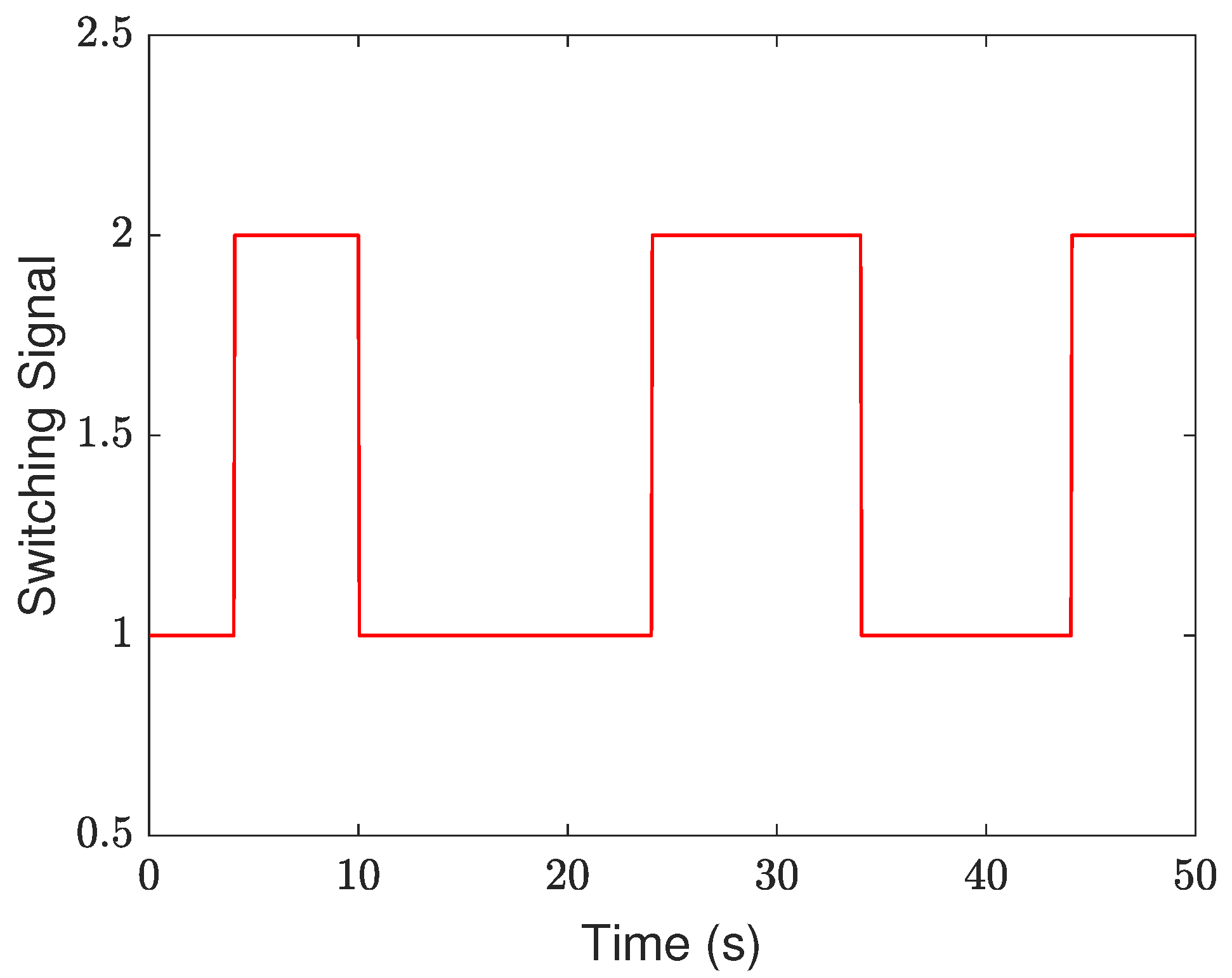
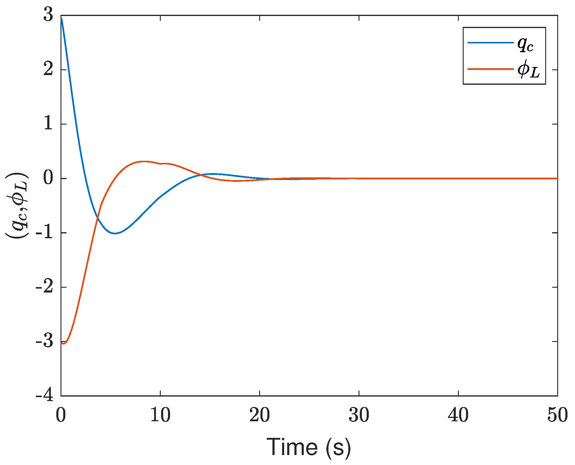
4. Simulation Example

This section is devoted to demonstrating the effectiveness of the developed ADBT control. We consider a switching resistor–inductor–capacitor (RLC) circuit [10] which is shown in Figure 1
z ˙ ( t ) = A ^ σ ( t ) z ( t ) + B ^ σ ( t ) u ( t ) ,
y ( t ) = C ^ z ( t ) ,
where z ( t ) = [ q c ϕ L ] T . q c represents the charge on the capacitor C j , j { 1 , 2 } . ϕ L indicates the flux through inductor L. The input voltage supply is noted as u ( t ) . σ ( t ) { 1 , 2 } indicates the switching signal. Let us assume that the model (29) is affected by the disturbance d ( t ) = e 2 t cos t .
Below, the model data are presented.
A ^ i = 0 1 L 1 C ^ i R L , B ^ 1 = 0 1 , B ^ 2 = 0.1 1 , B ^ d 1 = 0.5 0.3 , B ^ d 2 = 0.2 0.1 , C ^ = 1 0 , R = 3 , L = 2 , C 1 = 2 , C 2 = 4 , z ( t 0 ) = [ 3 3 ] T .
In the ADBT control designing scenario, by computing the conditions of Corollary 1, we set α = 0.8 , k c = 2 , A ^ e 1 = 31 , A ^ e 2 = 30 , B ^ F 1 = 30 , B ^ F 2 = 30 , C ^ e = 1 , K e 1 = K e 2 = 1.7 × 10 5 , K p 1 = 0 1 , K p 2 = 0 0.8 , L 1 = 2.3016 0.1620 T , L 2 = 3.1270 0.1765 T . The results indicate that the ADBT control strategy exhibits continuous behavior. Figure 2 illustrates the switching rule. In Figure 3, the amount of charge q c ( t ) stored in the capacitor and the magnetic flux passing through the inductance L are depicted. As shown in Figure 4, the power input source u ( t ) demonstrates that no bumping occurs.
To verify the effectiveness of the proposed ADBT control designing strategy, we use the sawtooth wave signal as a disturbance signal affecting the system. The sawtooth wave signal is commonly generated in many circuit models and is difficult to describe using general exogenous systems. From Figure 2, Figure 3 and Figure 4, one can clearly see that the proposed ADBT control strategy can estimate the sawtooth wave disturbance and, at the same time, achieve good BT performance. Hence, it can be concluded that the designed ADBT control strategy is effective.

5. Discussion

This paper proposes a new configuration for ADBT control via a switched EID methodology for switched linear systems. Although the ADBT control design problem has been solved in this paper, there still exist three aspects worth discussing. First, while our control method achieved good results in AD response, the convergence speed was slow. This is attributable to the choice of adjustable parameters and is worth studying in the future. Second, the ADBT control method in this paper is for switched linear systems; however, nonlinearities appear in most practical systems, such as spacecraft, robots and industrial processes. Therefore, this requires further research and discussion for switched nonlinear systems. A possible solution to the current implementation is to develop a switched nonlinear EID approach. We will leave this problem for future work. Additionally, we will try to apply the proposed control method to switched systems with more general structures and switched multi-agent systems.

6. Conclusions

In this paper, we studied the ADBT control design problem for switched linear systems. Firstly, a new switched EID estimator was established to estimate the impact of external disturbances for switched linear systems. Then, through the collaborative efforts of a switched EID estimator and a compensator, a continuous controller and a switching rule characterized by ADT were dual designed. Finally, by employing a switching RLC circuit model, we successfully demonstrated the effectiveness and practicality of the proposed ADBT control method. Through the simulation result, we showcased the great potential of the switched EID estimator in practical applications, offering valuable insights for future research and development. This research provides a new approach to solve the ADBT control design problem for switched linear systems. Moreover, notice that time delays and faults often occur in the practical systems. As an interesting research topic, the interaction between delays and the BT performance and the interaction between faults and BT performance need to be studied in the future.

Author Contributions

Conceptualization, Q.L.; methodology, Q.L. and J.W.; validation, J.W., Q.L. and P.Y.; formal analysis, Q.L.; investigation, J.W.; writing—original draft preparation, J.W.; writing—review and editing, Q.L.; visualization, Q.L.; supervision, P.Y.; funding acquisition, P.Y. All authors have read and agreed to the published version of the manuscript.

Funding

This research was funded by the National Natural Science Foundation of China grant number 62003010 and the R&D Program of Beijing Municipal Education Commission grant number KM202410005036.

Data Availability Statement

The data are contained within the article.

Conflicts of Interest

The authors declare no conflicts of interest.

References

  1. Zhang, J.; Huang, J.; Li, C. Distributed interval observers with switching topology design for cyber-physical systems. Mathematics 2024, 12, 163. [Google Scholar] [CrossRef]
  2. Ronanki, D.; Dasari, Y.; Williamson, S.S. Power electronics-based switched supercapacitor bank circuits with enhanced power delivery capability for pulsed power applications. In Proceedings of the 2021 IEEE Applied Power Electronics Conference and Exposition (APEC), Phoenix, AZ, USA, 14–17 June 2021; pp. 2271–2276. [Google Scholar]
  3. Shi, Y.; Sun, X. Bumpless transfer control for switched linear systems and its application to aero-engines. IEEE Trans. Circuits Syst. I Regul. Pap. 2021, 68, 2171–2182. [Google Scholar] [CrossRef]
  4. Zong, G.; Yang, D.; Lam, J.; Song, X. Fault-tolerant control of switched LPV systems: A bumpless transfer approach. IEEE/ASME Trans. Mechatron. 2021, 27, 1436–1446. [Google Scholar]
  5. Chen, W.; Yang, J.; Guo, L.; Li, S. Disturbance-observer-based control and related methods—An overview. IEEE Trans. Ind. Electron. 2015, 63, 1083–1095. [Google Scholar] [CrossRef]
  6. Han, J. From PID to active disturbance rejection control. IEEE Trans. Ind. Electron. 2009, 56, 900–906. [Google Scholar] [CrossRef]
  7. Guo, L.; Cao, S. Anti-Disturbance Control for Systems with Multiple Disturbances; CRC Press: Boca Raton, FL, USA, 2013. [Google Scholar]
  8. Guo, L.; Cao, S. Anti-disturbance control theory for systems with multiple disturbances: A survey. ISA Trans. 2014, 53, 846–849. [Google Scholar] [CrossRef] [PubMed]
  9. Yong, K.; Chen, M.; Wu, Q. Anti-disturbance control for nonlinear systems based on interval observer. IEEE Trans. Ind. Electron. 2019, 67, 1261–1269. [Google Scholar] [CrossRef]
  10. Zhao, Y.; Wu, D.; Xu, C.; Yu, S.; Liu, T.; Yang, D. Adaptive anti-disturbance bumpless transfer control for switched neural network systems with its application to switched circuit model. IEEE Trans. Circuits Syst. I Regul. Pap. 2024, 71, 411–420. [Google Scholar] [CrossRef]
  11. Liu, F.; Chen, M.; Shi, S.; Tao, L. Almost output regulation for turbofan switched systems under multi-source disturbances and time delay. Int. J. Robust Nonlinear Control 2024, 34, 378–396. [Google Scholar] [CrossRef]
  12. Yang, Y.; Zheng, W.; Liu, B. Adaptive anti-disturbance control for systems with saturating input via dynamic neural network disturbance modeling. IEEE Trans. Cybern. 2020, 52, 5290–5300. [Google Scholar]
  13. Zhang, S.; Zhang, B.; Li, X.; Wang, Z.; Qian, F. A method of enhancing fast steering mirror’s ability of anti-disturbance based on adaptive robust control. Math. Probl. Eng. 2019, 2019, 2152858. [Google Scholar] [CrossRef]
  14. Huang, Y.; Xue, W. Active disturbance rejection control: Methodology and theoretical analysis. ISA Trans. 2014, 53, 963–976. [Google Scholar] [CrossRef] [PubMed]
  15. Feng, H.; Guo, B. Active disturbance rejection control: Old and new results. Annu. Rev. Control 2017, 44, 238–248. [Google Scholar] [CrossRef]
  16. Du, Y.; Cao, W.; She, J.; Wu, M.; Fang, M.; Kawata, S. Disturbance rejection and robustness of improved equivalent-input-disturbance-based system. IEEE Trans. Cybern. 2021, 52, 8537–8546. [Google Scholar] [CrossRef]
  17. Yu, P.; Liu, K.Z.; Wu, M.; She, J. Improved Equivalent-Input-Disturbance Approach Based on H Control. IEEE Trans. Ind. Electron. 2019, 67, 8670–8679. [Google Scholar] [CrossRef]
  18. Mei, Q.; She, J.; Wang, F.; Nakanishi, Y.; Hashimoto, H.; Chugo, D. Disturbance rejection and control system design using 1-inverse-based equivalent-input-disturbance approach. IEEE Trans. Ind. Electron. 2022, 70, 1666–1675. [Google Scholar] [CrossRef]
  19. Zhang, L.; Xu, K.; Yang, J.; Han, M.; Yuan, S. Transition-dependent bumpless transfer control synthesis of switched linear systems. IEEE Trans. Autom. Control 2022, 68, 1678–1684. [Google Scholar] [CrossRef]
  20. Wu, T.; Zhu, Y.; Zhang, L.; Shi, P. Bumpless transfer model predictive control for Markov jump linear systems. IEEE Trans. Autom. Control 2023. [Google Scholar] [CrossRef]
  21. Yang, Y.; Huang, Z.; Zhang, P. Double-observer-based bumpless transfer control of switched positive systems. Mathematics 2024, 12, 1724. [Google Scholar] [CrossRef]
  22. Li, J.; Zhao, J. Bumpless transfer control for switched linear systems with bump induced event-triggered mechanism. J. Frankl. Inst. 2023, 360, 6081–6098. [Google Scholar] [CrossRef]
  23. Wang, Y.; Wang, X.; Zhao, Y.; Chen, Y.; Li, W. Finite-time event-triggered bumpless transfer control for switched systems. Int. J. Robust Nonlinear Control 2022, 32, 6962–6982. [Google Scholar] [CrossRef]
  24. Zong, G.; Huang, C.; Yang, D. Bumpless transfer fault detection for switched systems: A state-dependent switching approach. Sci. China Inf. Sci. 2021, 64, 172208. [Google Scholar] [CrossRef]
  25. Shi, J.; Zhao, J. State bumpless transfer control for a class of switched descriptor systems. IEEE Trans. Circuits Syst. I Regul. Pap. 2021, 68, 3846–3856. [Google Scholar] [CrossRef]
  26. Zhang, S.; Zhao, J. Dwell-Time-Dependent H Bumpless transfer control for discrete-time switched interval type-2 fuzzy systems. IEEE Trans. Fuzzy Syst. 2021, 30, 2426–2437. [Google Scholar] [CrossRef]
  27. Wen, S.X.; Shi, Y.; Pan, Z.R.; Sun, X.M. Practical bumpless transfer design for switched linear systems: Application to aeroengines. IEEE Trans. Ind. Inform. 2023, 19, 11910–11919. [Google Scholar] [CrossRef]
  28. Wu, F.; Wang, D.; Lian, J. Bumpless transfer control for switched systems via a dynamic feedback and a bump-dependent switching law. IEEE Trans. Cybern. 2022, 53, 5372–5379. [Google Scholar] [CrossRef]
  29. Shi, Y.; Zhao, J.; Sun, X. A bumpless transfer control strategy for switched systems and its application to an aero-engine. IEEE Trans. Ind. Inform. 2020, 17, 52–62. [Google Scholar] [CrossRef]
  30. Zhao, Y.; Zhao, J. H reliable bumpless transfer control for switched systems with state and rate constraints. IEEE Trans. Syst. Man Cybern. Syst. 2018, 50, 3925–3935. [Google Scholar] [CrossRef]
  31. Yang, D.; Zong, G.; Nguang, S.K.; Zhao, X. Bumpless transfer H anti-disturbance control of switching Markovian LPV systems under the hybrid switching. IEEE Trans. Cybern. 2020, 52, 2833–2845. [Google Scholar] [CrossRef]
  32. Levine, W.S. The Control Handbook; CRC Press: Boca Raton, FL, USA, 1996. [Google Scholar]
  33. Zhai, G.; Hu, B.; Kazunori, Y.; Michel, A. L2 gain analysis of switched systems with average dwell time. Trans. Soc. Instrum. Control Eng. 2000, 36, 937–942. [Google Scholar] [CrossRef]
Figure 1. A switching resistor–inductor–capacitor (RLC) circuit.
Mathematics 12 02307 g001
Figure 2. The switching signal σ ( t ) of the switching RLC circuit.
Mathematics 12 02307 g002
Figure 3. The charge q c ( t ) in the switched capacitor C σ ( t ) and the flux ϕ L ( t ) in the inductance L.
Mathematics 12 02307 g003
Figure 4. The input power source u ( t ) of the switching RLC circuit.
Mathematics 12 02307 g004
Disclaimer/Publisher’s Note: The statements, opinions and data contained in all publications are solely those of the individual author(s) and contributor(s) and not of MDPI and/or the editor(s). MDPI and/or the editor(s) disclaim responsibility for any injury to people or property resulting from any ideas, methods, instructions or products referred to in the content.

