
FMEA-TSTM-NNGA: A Novel Optimization Framework Integrating Failure Mode and Effect Analysis, the Taguchi Method, a Neural Network, and a Genetic Algorithm for Improving the Resistance in Dynamic Random Access Memory Components

Abstract
1. Introduction
2. Motivation for Problem Description
- (1)
- Thin film deposition operates by building up structures on a wafer using different types of materials in a layered manner. The first deposition method is chemical vapor deposition (CVD), which involves the use of corrosive gasses and chemicals which provide a thin covering to the wafers upon a chemical reaction. First of all, the gas containing target material is injected into the reaction chamber, and the wafer is located in this chamber. After that, by adjusting parameters such as the temperature and pressure, the gas molecules are prompted to chemically react with the aim of depositing the correct thin film material. These materials are deposited at the surface of the wafer, and after some time, they stack up and develop a film-like structure. The second deposition technique is physical vapor deposition (PVD), which is an advanced technology that transfers physical state materials into a gas or plasma state and deposits them on the surface of the wafer. Some PVD technologies are sputter deposition and evaporation deposition. Often, the material that is going to be deposited in any PVD technique becomes heated or is bombed first so that it can evaporate in the form of gas or plasma. These high-energy particles are then directed to the surface of the wafer, and in the process of collision, it is transformed into a thin film structure.
- (2)
- A microfabrication technique that is closely related to the manufacturing of a semiconductor is photolithography, where fine semiconductor circuit patterns are printed. The four sub-process operations are cleaning, photoresist application, exposure, and development, which the wafers undergo in the main process. Before photolithography is carried out, there is always a need to cleanse the wafer to remove any particles which may hinder the photolithography process. The cleaning methods which are employed for the wafers are solution washing, high-pressure water cleaning, and ultrasonic cleaning. Then, a layer of material known as the photoresist, a polymer that can be dissolved by exposure to light of a specific wavelength, is formed on the wafer’s surface. The photoresist is typically used and can be dispensed uniformly on the surface of the wafer by the spin-coating method. Incidentally, the photomask may be exposed to a light source of a given wavelength with the intention of projecting some patterns on the surface of the wafer. These light rays will only pass through the parts of the photo res dose where the thickness of the photo res dose will be consistent with that of the underlying layer, and they will not pass through areas where the layers of the photo res dose will have to be stripped off. Finally, the wafer is put into a developer solution where the other parts of the photoresist layer exposed to light are dissolved. This method is called positive photoresist development, where the exposed layer of the photoresist becomes the pattern in the shape and size of the required design.
- (3)
- In the etching process, the un-masked areas in the wafer are chemically or physically etched to make the circuit structure of the required semiconductor materials by erasing the unwanted areas. Dry etching can be described as the technique of taking material on a wafer’s surface by means of gas plasma or reactive plasma. In the course of the dry etching process, the wafer is located in the vacuum chamber, and a gas flow containing the reactive gas is used. Finally, the gas experiences a reaction under plasma excitation, which allows the removal of material deposited on the surface of the wafer. Wet etching also involves the process of removing material on the wafer’s surface by an actual chemical process which occurs in a liquid medium. In the wet etching process, the wafer is completely submerged in a bath which contains an etching solution. The etching solution decomposes chemically with the materials on the wafer, and this results in their removal.
- (4)
- The polishing process is employed in the manufacturing process to planarize the wafer. The steps include coarse polishing, fine polishing, cleaning, and inspection. First, the wafer is placed on the rotating polishing disk, and then, with the polishing particles, a preliminary polish is performed to minimize surface roughness, protrusions, and depressions on the wafer. However, an additional step of planarization is required to further smooth the wafer’s surface. This step uses the smallest polishing particles and the highest pressure to achieve the desired flatness. During the polishing process of ion-implanted silicon wafers, polish debris and dirt are extensively produced. Therefore, it is necessary to perform chemical or physical cleaning on the wafer’s surface to meet the required cleanliness and smoothness conditions, as the presence of high amounts of polishing powder and dirt may hinder this. After polishing and cleaning, there may still be slight roughness or scratches on the wafer’s surface in terms of flatness. To further enhance the flatness and surface quality of the wafer, other methods like chemical mechanical polishing or even conventional mechanical polishing can be employed. Lastly, the wafers are required to undergo a final cleaning step to ensure that the entire surface is free of any dirt and polishing residue and to verify that the wafer’s flatness meets the required standards.
3. Methodology
3.1. Taguchi Method
- (1)
- Problem Definition and Objective Setting: The output attributes and the inputs related to the performance, for instance, the quality of the product, are determined. When writing down the specifications, it is necessary to state the target performance issues of the system as well as define its target values or response curves if any.
- (2)
- Experimental Design: The control factors that define the system’s performance are chosen and their possible levels are defined. As noted in the Taguchi method, it is possible to test more than one input factor. It is recommended to apply Taguchi’s orthogonal array to build an experimental matrix that would cover all possible combinations of the factor level settings.
- (3)
- Experimentation and Data Collection: Experiments are performed on the basis of designed specifications of the input and output characteristics. For each run of the experiment, the response values (the output characteristics) are documented.
- (4)
- Data Analysis: Regarding quality characteristics, the SN is used in order to determine the stability of the system. On that basis, the key factors that play a crucial role in shaping the output characteristics are defined, and their importance is assessed.
- (5)
- Optimization and Validation: Multiple comparison is performed using the post hoc test to define the best level of the factor on the basis of the mean value of the SN ratio and the ANOVA. Using a practical test or more precise factor confirmation experiments, the advantages of the selected factor setting are confirmed.
- (1)
- Define the Problem
- −
- To ensure clarity on what the experiment would set out to achieve, the following is carried out:
- −
- The output (response) characteristics, which should be optimized, are identified.
- −
- The relations between the input factors (variables) and output are determined.
- (2)
- Select Factors and Levels
- −
- The research objectives and questions or hypotheses are formulated for the control factors for the study.
- −
- The method used to measure each factor is described.
- (3)
- Design the Experiment
- −
- An appropriate orthogonal array is chosen depending on the factor number and level number.
- −
- The experimental matrix is developed through the choice of orthogonal array, chosen above.
- (4)
- Conduct the Experiments
- −
- The experiments are carried out as per the design matrix laid out above.
- −
- A record of the final output values obtained at the end of each of the experimental runs is made.
- (5)
- Analyze the Data
- −
- The signal-to-noise (SN) ratio values of each experimental runs are determined.
- −
- The trends in the SN ratios could be analyzed in order to obtain an idea about the performance of the system.
- −
- An analysis of variance (ANOVA) test is performed to determine the contribution of each factor.
- (6)
- Optimize the Process
- −
- The combination of factor levels is determined, which could be considered as optimal according to the analysis.
- −
- All of the process parameters are changed to the best possible values.
3.2. Artificial Neural Network
- (1)
- Initialize the Network
- −
- The number of neurons in the input layer, hidden layer, and output layer is decided.
- −
- Initial values of the weights and biases are assigned with respect to each neuron (these may preferably be assigned randomly).
- (2)
- Forward Propagation
- −
- The following is carried out for each input sample:
- Input Layer:
- −
- Let the input layer take in the input data.
- Hidden Layer:
- −
- The following is carried out for each hidden layer neuron:
- −
- The weighted sum of inputs is found, and bias is added to them.
- −
- An activation function, such as ReLU, sigmoid, or other, is applied to the sum.
- Output Layer:
- −
- The following is carried out for each output neuron:
- −
- The sum of the products of the weight in the connection between two neurons and the hidden layer’s output plus the bias term are found.
- −
- An activation function is applied to the sum to come up with the final output.
- (3)
- Calculate Loss
- −
- The difference between the predicted output and the target output is found by using a loss function, e.g., mean squared error or cross entropy.
- (4)
- Backpropagation
- −
- The backpropagation algorithm is used to determine the gradient with respect to all of the weights and biases of the network.
- −
- The following is carried out for each layer:
- The derivative of the activation function is determined.
- The first-order derivative of the loss with the weights and the biases is calculated.
- The weights and the biases are updated according to the gradients calculated at the beginning of the current iteration.
- (5)
- Iterate
- −
- Steps 2–4 are repeated for a certain number of epochs or until the loss function falls within an acceptable range.
- (6)
- Output the Results
- −
- Once training is complete, the network can be used to predict the outputs of other inputs.
- −
- The effectiveness of the network is assessed using a testing dataset.
3.3. Genetic Algorithm
- (1)
- Initialize population: First, a set of potential solutions is randomly created, which forms the first generation of the population.
- (2)
- Evaluate population: The performance value of each possible solution is measured, and it is referred to as the fitness function value.
- (3)
- Select parents: Some solutions with high fitness function values are chosen as parents. In most cases, roulette wheel selection or the elite preservation strategy is employed for the selection of parents.
- (4)
- Crossover: Two parents are randomly chosen to crossover in order to create two new chromosomes.
- (5)
- Mutation: Sometimes, it is necessary to mutate the offspring with some certain probability in order to avoid falling into local optima.
- (6)
- Select next generation: Numbers of offspring and parents are chosen as the next generation of the population.
- (7)
- Iteration steps 2 to 6 are performed over and over until either the condition for convergence is reached or the maximum number of iterations has been exhausted.
- (8)
- Finally, the candidate with the highest objective value is chosen as the global optimal solution to the presented mathematical model.
- (1)
- Initialize Population
- −
- The first generation of the candidate solutions, commonly known as the chromosomes, is produced.
- −
- Each chromosome is a candidate solution, and most commonly, these chromosomes are stored as binary strings of numbers and real numbers, amongst other formats.
- (2)
- Evaluate Fitness
- −
- The following is carried out for each chromosome in the population:
- The chromosome is translated into the solution on the chromosome it represents.
- Another measure of the solution obtained is determined by considering the goal or objective function of the problem.
- (3)
- Selection
- −
- Parent chromosomes in the current population are chosen using the fitness measure defined.
- −
- Higher fitness enhances the likelihood of selection, for example, by means of roulette wheel and tournament selections.
- (4)
- Crossover
- −
- The following is carried out for each pair of selected parents:
- The crossover point(s) is selected as a victim.
- Equal segments of the parent’s chromosomes are exchanged at crossover point(s) to form the offspring commonly referred to as children.
- −
- With a certain crossover probability, a crossover operation should be performed in order to generate new offsprings.
- (5)
- Mutation
- −
- The following is carried out for each offspring:
- A possibility of mutation is created that will cause some arbitrary change to some genes in the chromosome.
- It must be ensured that mutation contributes to the creation of diversity but does not interfere with searching.
- (6)
- Create New Population
- −
- The waiting list state is populated by replacing the old population with the new population, which is the offspring.
- −
- Optionally, some of the chromosomes with good quality are transferred to the old population in order to guarantee the existence of good solutions.
- (7)
- Iterate
- −
- Steps 2–6 are repeated for a specified number of generations or until a termination condition is met (e.g., the fitness threshold or maximum number of generations).
- (8)
- Output the Best Solution
- −
- After the final generation, the chromosome with the highest fitness is identified and output as the best solution found by the algorithm.
4. The Proposed Methodology
- Defining the problem: In this step, the existing abnormal phenomena and their yield loss rate of defects in the case study are described. The manufacturing process that may be causing the abnormalities is identified based on the adverse phenomena observed.
- Using FMEA to assess production attributes: FMEA was used to assess the production attributes affecting memory component resistance in thin film deposition, etching, plating, and polish processes. Relevant production attribute setting is then identified to improve the average resistance of DRAM components in the medical equipment through the optimization of these production attributes.
- Applying first stage Taguchi method to find important attributes: In this step, we will use the Taguchi method L12(211) orthogonal array to collect experimental data. We will then use attribute response tables, attribute response charts, and ANOVA (analysis of variance) tables to analyze the data and identify important production attributes that affect the average resistance of DRAM components. At present, many researchers have used Taguchi method to assist in the optimization and improvement of engineering problems. Gao and Zhou (2024) employs the Taguchi Method to conduct sensitivity analysis on operating parameters for a proton exchange membrane fuel cell (PEMFC) combined heat and power (CHP) cogeneration system in variable climate regions, proposing cost-effective strategies for electricity- and heat-dominated outputs [25]. Xie et al. (2024) used the Taguchi method to explore key parameters in pure waterjet surface treatment of Ti6Al4V specimens, emphasizing the significance of operation pressure for biomaterial surface fine-tuning [26]. Tanürün et al. (2024) employed the Taguchi method to optimize Vertical Axis Wind Turbine (VAWT) performance with an adaptive flap design, achieving a 74.01% increase in power coefficient (CP) compared to conventional VAWTs, with flap position identified as the most influential factor [27]. Lu et al. (2024) used the Taguchi method to optimize CO2 laser polishing of fused silica, revealing laser beam scanning speed as a crucial factor, resulting in a substantial reduction in surface roughness from Ra = 0.157 μm to 0.005 μm [28]. Yang et al. (2024) utilized the Taguchi method and Gray relation analysis to identify the optimal design parameters (perforation length, height, and tilt angle) for slit fins with lateral perforations, achieving the highest j-factor and lowest f-factor [29]. Based on the empirical evidence presented in the literature, it is clear that Taguchi’s experimental design can effectively assist researchers in identifying important parameters across various fields and finding optimal parameter settings for different engineering problems.
- Applying second stage Taguchi method to recollect data and find out the optimal attribute setting: To collect experimental data, we used the Taguchi method L18(21 × 37) orthogonal array. We conducted a second Taguchi method in the production attribute region, with the aim of recollecting experimental data that could potentially contain optimal solutions using the L18(21 × 37) orthogonal array. We analyzed the collected data using attribute response tables, attribute response charts, and ANOVA table to determine the optimal attribute setting in the region.
- Using artificial neural networks to build a model: To construct the relationship between the important production attributes and the resistance value of DRAM components of medical equipment in the L18(21 × 37) orthogonal array, an artificial neural network can be used. Recent studies frequently use neural networks to establish relationships between production attributes and response variables, and subsequently use these models to determine the optimal attribute settings and enhance product quality. Acharjee et al. (2024) developed two artificial neural network based models (W-ANN and H-ANN) for predicting dynamic modulus in Colombian hot-mix asphalt mixtures, outperforming previous models and providing practical tools for pavement design with reduced testing requirements [30]. Liu (2024) presents a sensor array based on noble metal-doped In2O3, employing a back propagation neural network (BPNN) integrated with the whale optimization algorithm (WOA) for anti-interference detection of mixed NOX, achieving quantitative prediction of components in the presence of cross interference [31]. Mudawar et al. (2024) employed artificial neural networks to predict heat transfer and critical heat flux (CHF) in both microgravity and Earth gravity [32]. Sayed et al. (2024) applied artificial intelligence (ANN and FBI) to optimize yeast and wastewater concentrations in a microalgae microbial fuel cell, achieving significant improvements in power density and COD removal [33]. Sanni et al. (2024) employed an adaptive neuro-fuzzy inference system (ANFIS) to model the corrosion rate of AISI 316 stainless steel under various inhibitor dosages and schedules, achieving superior prediction accuracy [34].
- Adopting genetic algorithm to identify the best production attribute setting: The genetic algorithm will be used to identify the best setting of production attribute levels across the entire production attribute region. Many researchers have also confirmed the feasibility of the genetic algorithm. Park et al. (2024) integrated genetic algorithms and deep learning to enhance the I-V modeling of DRAM transistors, addressing limitations of the BSIM model and accurately modeling devices with hot-carrier degradation effects [35]. Mukhanov et al. (2020) introduced DStress, a framework using genetic algorithms to identify worst-case DRAM error patterns, enhancing testing by detecting critical reliability issues and improving testing mechanisms [36]. Leu et al. (2021) used genetic algorithms to reduce thickness deviation in DRAM manufacturing. The approach successfully decreased deviation from 45.0 to 12.9 Å [37]. Babu et al. (2024) proposed a novel IoT network optimization strategy using a genetic algorithm (GA) for energy efficiency and mixed integer linear programming (MILP) for node deployment, with blockchain enhancing data privacy; outperforming existing models in network lifetime and throughput [38]. Nigam et al. (2024) accelerated molecular design using a genetic algorithm and an artificial neural network, identifying over 10,000 potential organic emitters with inverted singlet-triplet gaps (INVEST) and appreciable fluorescence rates for potential use in new-generation organic light-emitting diodes [39]. Wang et al. (2024) applied an improved genetic algorithm for optimal scheduling in hybrid energy ship power systems, reducing costs and environmental impacts [40]. Bhat et al. (2024) enhanced aluminum alloy design using machine learning, incorporating data-driven classes and genetic algorithms for feature optimization, achieving improved tensile strength and elongation predictions [41]. Ildarabadi et al. (2024) applied a genetic algorithm with elitism mechanism to optimize the cost of restoring power to a distribution network after disasters by building Tie-lines between damaged and healthy sections [42]. GA is an optimization technique that can be applied to a wide range of engineering problem areas. Therefore, it is favored by researchers who want to find optimal solutions to complex problems.
- Performing confirmation experiments and comparisons: After identifying the optimal settings for production attributes, confirmation experiments are carried out to confirm the efficacy of the suggested methodology., and the results are compared with the average resistance of DRAM components before improvement to confirm the effectiveness of the improvements.
- (1)
- Define the problem.
- −
- The various abnormal phenomena and the yield loss rate of defects that is associated with it are explained.
- −
- The manufacturing processes that is responsible for the formation of such abnormalities is determined.
- (2)
- Examine the possibility of failure in the future and identify product attributes in the FMEA.
- −
- The FMEA is used to assess the production characteristics that impact memory component resistance.
- −
- The critical production attributes of thin film deposition, etching and plating, and polishing are determined.
- −
- The optimal settings of the production attributes that will cause the DRAM components to have an average resistance greater than past records are determined.
- (3)
- Use the first stage of the Taguchi method.
- −
- The L12(211) orthogonal array is chosen to plan the experiments.
- −
- Research is conducted and information is obtained.
- −
- The analysis of attribute data can be carried out with the help of attribute response tables, response chars, and an ANOVA in order to determine important production attributes influencing DRAM component resistance.
- (4)
- Use the second stage of the Taguchi method.
- −
- Further experimentation should be carried out using the L18(21 × 37) orthogonal array.
- −
- More tests should be conducted in order to gather information on the area of important attributes.
- −
- This means that one has to perform the analysis of the obtained data to identify the appropriate values of production attributes.
- (5)
- Develop a model employing artificial neural networks.
- −
- An artificial neural network is performed with the dependent variable of resistance values of DRAM components, with the independent variables being the important production attributes.
- −
- The neural network model should be trained and validated using the experimental data collected from the second stage of the Taguchi method.
- (6)
- Optimize the production attribute settings with the genetic algorithm.
- −
- A genetic algorithm search is performed regarding the overall attribute region of the production attribute in order to obtain the global optima of the attribute settings.
- −
- The suitability of several contexts is analyzed and the most appropriate one is determined.
- (7)
- Confirmation experiments and comparison.
- −
- Confirmation experiments are carried out using the best production attribute settings which were found.
- −
- The findings are assessed with pre-change data to ensure that the above proposed methodology has a powerful impact.
- −
- Details, especially the outline of the results of their work, are determined with an emphasis on increases in the average resistance of DRAM parts.
5. Case Study
Details Content of the Proposed Methodology
- (1)
- Problem Definition
- (2)
- Using FMEA to assess production attributes
- (3)
- Applying first stage Taguchi method to find important attributes
- (4)
- Applying second stage Taguchi method to recollect data and find out the optimal attribute setting
- (5)
- Using artificial neural networks to build a model
- (6)
- Adopting genetic algorithm to identify the best production attribute setting
- (7)
- Performing confirmation experiments and comparisons
6. Numerical Simulations and Discussion
- (a)
- Analysis of variance (ANOVA)
- (b)
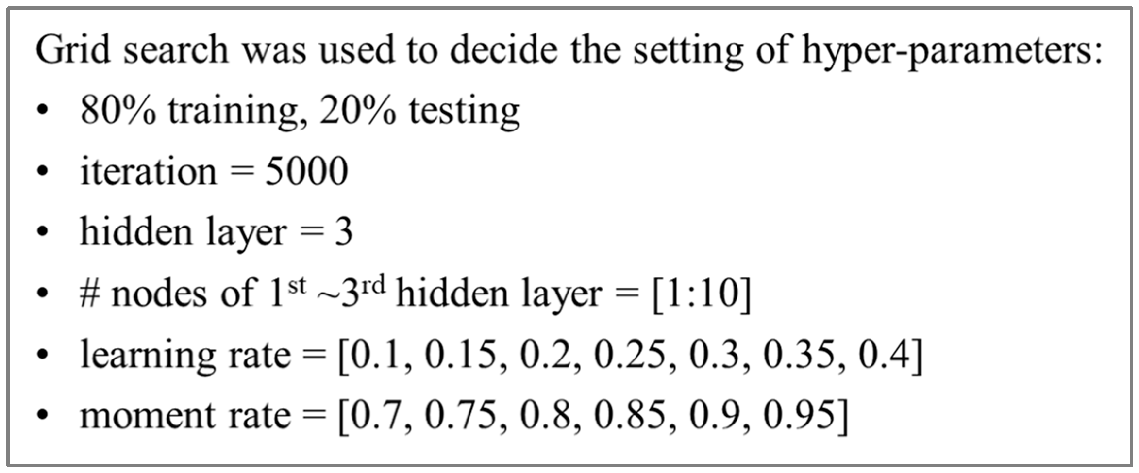
- Neural networks (NN)
- (c)
- Genetic algorithm (GA)
7. Conclusions
Author Contributions
Funding
Data Availability Statement
Conflicts of Interest
References
- Mathews, K. COVID-19’s Impact on the Semiconductor Industry. 2021. Available online: https://kidder.com/trend-articles/covid-19s-impact-on-the-semiconductor-industry/ (accessed on 30 August 2024).
- Kim, K. The smallest engine transforming humanity: The past, present, and future. In Proceedings of the 2021 IEEE International Electron Devices Meeting (IEDM), San Francisco, CA, USA, 11–16 December 2021. [Google Scholar] [CrossRef]
- Cohen, S.; Hershcovitch, M.; Taraz, M.; Kißig, O.; Wood, A.; Waddington, D.; Chin, P.; Friedrich, T. Drug repurposing using link prediction on knowledge graphs with applications to non-volatile memory. In Complex Networks & Their Applications X: Volume 2, Proceedings of the Tenth International Conference on Complex Networks and Their Applications COMPLEX NETWORKS 2021; Springer International Publishing: Cham, Switzerland, 2022; Volume 1073, pp. 742–753. [Google Scholar] [CrossRef]
- Shiratake, S. Scaling and performance challenges of future DRAM. In Proceedings of the 2020 IEEE International Memory Workshop (IMW), Dresden, Germany, 17–20 May 2020. [Google Scholar]
- Arpaia, P.; Cataldo, A.; Criscuolo, S.; De Benedetto, E.; Masciullo, A.; Schiavoni, R. Assessment and Scientific Progresses in the Analysis of Olfactory Evoked Potentials. Bioengineering 2022, 9, 252. [Google Scholar] [CrossRef]
- Rahman, H.; Bukht, T.F.N.; Imran, A.; Tariq, J.; Tu, S.; Alzahrani, A. A Deep Learning Approach for Liver and Tumor Segmentation in CT Images Using ResUNet. Bioengineering 2022, 9, 368. [Google Scholar] [CrossRef] [PubMed]
- Chen, T.C.T. Sustainable smart healthcare applications: Lessons learned from the COVID-19 pandemic. In Sustainable Smart Healthcare: Lessons Learned from the COVID-19 Pandemic; Springer Nature: Cham, Switzerland, 2023; pp. 65–92. [Google Scholar] [CrossRef]
- Kim, D.H.; Kwon, H.J.; Bae, S.J. DRAM circuit and process technology. In Semiconductor Memories and Systems; Woodhead Publishing: Sawston, UK, 2022; pp. 87–117. [Google Scholar] [CrossRef]
- Kim, S.S.; Yong, S.K.; Kim, W.; Kang, S.; Park, H.W.; Yoon, K.J.; Sheen, D.S.; Lee, S.; Hwang, C.S. Review of semiconductor flash memory devices for material and process issues. Adv. Mater. 2023, 35, 2200659. [Google Scholar] [CrossRef]
- Linliu, K. DRAM (Dynamic Random Access Memory) Process Flow; Independently Published: 2020. Available online: https://www.amazon.com/Dynamic-Random-Access-Memory-Process/dp/B084DLVSSP (accessed on 12 August 2024).
- Xiao, H. 3D IC Devices, Technologies, and Manufacturing; SPIE Press Monographs: Washington, WA, USA, 2016. [Google Scholar]
- Prince, B. Semiconductor Memories: A Handbook of Design, Manufacture and Application, 2nd ed.; John Wiley & Sons: New York, NY, USA, 1996. [Google Scholar]
- Kuo, Y. Thin Film Transistor Technologies VI: Proceedings of the International Symposium; The Electrochemical Society: New Jersey, NJ, USA, 2003. [Google Scholar]
- Phadke, M.S. Quality Engineering Using Robust Design; Prentice-Hall: New Jersey, NJ, USA, 1989. [Google Scholar]
- Fowlkes, W.Y.; Creveling, C.M. Engineering Methods for Robust Product Design; Addison-Wesley Publishing Company: Boston, MA, USA, 1995. [Google Scholar]
- Su, C.T. Quality Engineering: Off-Line Methods and Applications, 1st ed.; CRC Press: Boca Raton, FL, USA, 2013. [Google Scholar]
- Ross, P.J. Taguchi Techniques for Quality Engineering: Loss Function, Orthogonal Experiments, Parameter and Tolerance Design, 2nd ed.; McGraw-Hill: New York, NY, USA, 1996. [Google Scholar]
- Rosenblatt, F. Principles of Neurodynamics: Perceptrons and the Theory of Brain Mechanisms; Spartan Books: New York, NY, USA, 1962. [Google Scholar]
- Stern, H.S. Neural networks in applied statistics. Technometrics 1996, 38, 205–214. [Google Scholar] [CrossRef]
- McClelland, J.L.; Rumelhart, D.E. Explorations in Parallel Distributed Processing: A Handbook of Models, Programs, and Exercises, 1st ed.; MIT Press: London, UK, 1989. [Google Scholar]
- Fausett, L. Fundamentals of Neural Networks: An Architecture, Algorithms, and Applications; Prentice Hall: New Jersey, NJ, USA, 1994. [Google Scholar]
- Hagan, M.T.; Demuth, H.B.; Beale, M. Neural Network Design; PWS: Boston, MA, USA, 1995. [Google Scholar]
- Goldberg, D.E. Genetic Algorithm in Search, Optimization and Machine Learning, 1st ed.; Addison-Wesley: New York, NY, USA, 1989. [Google Scholar]
- Renders, J.M.; Flasse, S.P. Hybrid methods using genetic algorithms for global optimization. IEEE Trans. Syst. Man Cybern. Part B (Cybern.) 1966, 26, 243–258. [Google Scholar] [CrossRef]
- Gao, B.; Zhou, Y. In-field experimental study and multivariable analysis on a PEMFC combined heat and power cogeneration for climate-adaptive buildings with taguchi method. Energy Convers. Manag. 2024, 301, 118003. [Google Scholar] [CrossRef]
- Xie, J.; Qiao, Y.; Qi, Y.; Xu, Q.; Shemtov-Yona, K.; Chen, P.; Rittel, D. Application of the Taguchi method to areal roughness-based surface topography control by waterjet treatments. Appl. Surf. Sci. Adv. 2024, 19, 100548. [Google Scholar] [CrossRef]
- Tanürün, H.E. Improvement of vertical axis wind turbine performance by using the optimized adaptive flap by the Taguchi method. Energy Sources Part A Recovery Util. Environ. Eff. 2024, 46, 71–90. [Google Scholar] [CrossRef]
- Lu, G.; Li, X.; Wang, D.; Wang, K. Process Parameter Optimization for CO2 Laser Polishing of Fused Silica Using the Taguchi Method. Materials 2024, 17, 709. [Google Scholar] [CrossRef]
- Yang, P.; Wang, L.; Qing, T.; Liu, Y. Multi-objective optimization of geometrical parameters of laterally perforated on silt fin by gray relation analysis based on Taguchi method. Int. J. Therm. Sci. 2024, 196, 108705. [Google Scholar] [CrossRef]
- Acharjee, P.K.; Souliman, M.I.; Freyle, F.; Fuentes, L. Development of dynamic modulus prediction model using artificial neural networks for colombian mixtures. J. Transp. Eng. Part B Pavements 2024, 150, 04023038. [Google Scholar] [CrossRef]
- Liu, Y.; Yang, Z.; Huang, L.; Zeng, W.; Zhou, Q. Anti-interference detection of mixed NOX via In2O3-based sensor array combining with neural network model at room temperature. J. Hazard. Mater. 2024, 463, 132857. [Google Scholar] [CrossRef] [PubMed]
- Mudawar, I.; Darges, S.J.; Devahdhanush, V.S. Prediction technique for flow boiling heat transfer and critical heat flux in both microgravity and Earth gravity via artificial neural networks (ANNs). Int. J. Heat Mass Transfer. 2024, 220, 124998. [Google Scholar] [CrossRef]
- Sayed, E.T.; Rezk, H.; Abdelkareem, M.A.; Olabi, A.G. Artificial neural network based modelling and optimization of microalgae microbial fuel cell. Int. J. Hydrogen Energy 2024, 52, 1015–1025. [Google Scholar] [CrossRef]
- Sanni, O.; Adeleke, O.; Ukoba, K.; Ren, J.; Jen, T.C. Prediction of inhibition performance of agro-waste extract in simulated acidizing media via machine learning. Fuel 2024, 356, 129527. [Google Scholar] [CrossRef]
- Park, J.H.; Kim, J.N.; Lee, S.; Kim, G.J.; Lee, N.; Baek, R.H.; Kim, D.H.; Kim, C.; Kang, M.; Kim, Y. Current-Voltage Modeling of DRAM Cell Transistor Using Genetic Algorithm and Deep Learning. IEEE Access 2024, 12, 23881–23886. [Google Scholar] [CrossRef]
- Mukhanov, L.; Nikolopoulos, D.S.; Karakonstantis, G. Dstress: Automatic synthesis of dram reliability stress viruses using genetic algorithms. In Proceedings of the 2020 53rd Annual IEEE/ACM International Symposium on Microarchitecture (MICRO), Athens, Greece, 17–21 October 2020; pp. 298–312. [Google Scholar] [CrossRef]
- Leu, Y.; Lin, C.M.; Yang, W.N. Reducing Thickness Deviation of W-Shaped Structures in Manufacturing DRAM Products Using RSM and ANN_GA. IEEE Trans. Compon. Packag. Manuf. Technol. 2021, 11, 899–910. [Google Scholar] [CrossRef]
- Babu, R.M.; Satamraju, K.P.; Gangothri, B.N.; Malarkodi, B.; Suresh, C.V. A hybrid model using genetic algorithm for energy optimization in heterogeneous internet of blockchain things. Telecommun. Radio Eng. 2024, 83, 1–16. [Google Scholar] [CrossRef]
- Nigam, A.; Pollice, R.; Friederich, P.; Aspuru-Guzik, A. Artificial design of organic emitters via a genetic algorithm enhanced by a deep neural network. Chem. Sci. 2024, 15, 2618–2639. [Google Scholar] [CrossRef]
- Wang, X.; Zhu, H.; Luo, X.; Chang, S.; Guan, X. An energy dispatch optimization for hybrid power ship system based on improved genetic algorithm. Proc. Inst. Mech. Eng. Part A J. Power Energy 2024, 238, 348–361. [Google Scholar] [CrossRef]
- Bhat, N.; Barnard, A.S.; Birbilis, N. Inverse Design of Aluminium Alloys Using Genetic Algorithm: A Class-Based Workflow. Metals 2024, 14, 239. [Google Scholar] [CrossRef]
- Ildarabadi, R.; Lotfi, H.; Hajiabadi, M.E. Resilience enhancement of distribution grids based on the construction of Tie-lines using a novel genetic algorithm. Energy Syst. 2024, 15, 371–401. [Google Scholar] [CrossRef]
- Kroese, D.P.; Brereton, T.; Taimre, T.; Botev, Z.I. Why the Monte Carlo method is so important today. Wiley Interdiscip. Rev. Comput. Stat. 2014, 6, 386–392. [Google Scholar] [CrossRef]
- St»Hle, L.; Wold, S. Analysis of variance (ANOVA). Chemom. Intell. Lab. Syst. 1989, 6, 259–272. [Google Scholar] [CrossRef]


| No | A | B | C | D | E | F | G | H | I | J | K |
|---|---|---|---|---|---|---|---|---|---|---|---|
| 1 | 1 | 1 | 1 | 1 | 1 | 1 | 1 | 1 | 1 | 1 | 1 |
| 2 | 1 | 1 | 1 | 1 | 1 | 2 | 2 | 2 | 2 | 2 | 2 |
| 3 | 1 | 1 | 2 | 2 | 2 | 1 | 1 | 1 | 2 | 2 | 2 |
| 4 | 1 | 2 | 1 | 2 | 2 | 1 | 2 | 2 | 1 | 1 | 2 |
| 5 | 1 | 2 | 2 | 1 | 2 | 2 | 1 | 2 | 1 | 2 | 1 |
| 6 | 1 | 2 | 2 | 2 | 1 | 2 | 2 | 1 | 2 | 1 | 1 |
| 7 | 2 | 1 | 2 | 2 | 1 | 1 | 2 | 2 | 1 | 2 | 1 |
| 8 | 2 | 1 | 2 | 1 | 2 | 2 | 2 | 1 | 1 | 1 | 2 |
| 9 | 2 | 1 | 1 | 2 | 2 | 2 | 1 | 2 | 2 | 1 | 1 |
| 10 | 2 | 2 | 2 | 1 | 1 | 1 | 1 | 2 | 2 | 1 | 2 |
| 11 | 2 | 2 | 1 | 2 | 1 | 2 | 1 | 1 | 1 | 2 | 2 |
| 12 | 2 | 2 | 1 | 1 | 2 | 1 | 2 | 1 | 2 | 2 | 1 |
| No | Process | Attributes | Severity | Occurrence | Detection | RPN |
|---|---|---|---|---|---|---|
| 1 | SiCo TF-depo | HtrSpace1/HtrSpace2 | 3 | 4 | 4 | 48 |
| 2 | Pressure (Torr) | 4 | 3 | 3 | 36 | |
| 3 | RF1Time/RF2Time (s) | 7 | 8 | 2 | 112 | |
| 4 | HighFreqRF1Pwr/HighFreqRF2Pwr (W) | 3 | 4 | 3 | 36 | |
| 5 | LowFreqRF1Pwr/LowFreqRF2Pwr (W) | 5 | 4 | 3 | 60 | |
| 6 | OMCTS Flow Set (mgm) | 2 | 3 | 2 | 12 | |
| 7 | HE_OMCTS Flow Set (sccm) | 3 | 4 | 4 | 48 | |
| 8 | O2 Flow Set (sccm) | 2 | 4 | 4 | 32 | |
| 9 | ARC-LTO etch | E.Time (s) | 3 | 4 | 2 | 24 |
| 10 | Pressure (mTorr) | 9 | 8 | 3 | 216 | |
| 11 | RF Power 60 MHz | 3 | 3 | 4 | 36 | |
| 12 | RF Power 13.56 MHz | 2 | 4 | 4 | 32 | |
| 13 | HV (-V) | 3 | 2 | 3 | 18 | |
| 14 | Gas O2 (sccm) | 5 | 3 | 4 | 60 | |
| 15 | Gas CF4 (sccm) | 2 | 3 | 4 | 24 | |
| 16 | Gas CHF3 (sccm) | 4 | 2 | 4 | 32 | |
| 17 | Gas ratio (center%) | 2 | 3 | 4 | 24 | |
| 18 | Temp Top (°C) | 4 | 4 | 3 | 48 | |
| 19 | Temp Wall (°C) | 3 | 4 | 3 | 36 | |
| 20 | Temp Bottom (°C) | 3 | 4 | 3 | 36 | |
| 21 | Oxide-SiCO etch | E.Timt (s) | 7 | 7 | 3 | 147 |
| 22 | Pressure (mTorr) | 3 | 5 | 3 | 45 | |
| 23 | RF Power (W) 60 MHz | 3 | 4 | 4 | 48 | |
| 24 | RF Power (W) 13.56 MHz | 3 | 3 | 4 | 36 | |
| 25 | HV (-V) | 3 | 3 | 3 | 27 | |
| 26 | Gas O2 (sccm) | 5 | 3 | 4 | 60 | |
| 27 | Gas CF4 (sccm) | 2 | 4 | 4 | 32 | |
| 28 | Gas CHF3 (sccm) | 9 | 5 | 4 | 180 | |
| 29 | Gas ratio (center%) | 8 | 4 | 4 | 128 | |
| 30 | Temp Top (°C) | 5 | 3 | 3 | 45 | |
| 31 | Temp Wall (°C) | 2 | 3 | 3 | 18 | |
| 32 | Temp Bottom (°C) | 3 | 3 | 3 | 27 | |
| 33 | Cu polish | Head States: Zone 1–5 (psi) | 6 | 8 | 4 | 192 |
| 34 | End Step Criteria: Max Time (s) | 7 | 8 | 2 | 112 |
| Factor | Depo Time (s) | Depo He Flow (sccm) | Depo O2 Flow (sccm) | ARC-LTO Etch Time (s) | ARC-LTO Etch Pressure (mTorr) | Ox-SiCO Etch Time (s) | Ox-SiCO Gas Ratio (%) | Ox-SiCO CHF3 Flow (sccm) | Polish Time (s) | Polish Pressure (psi) |
|---|---|---|---|---|---|---|---|---|---|---|
| A | B | C | D | E | F | G | H | I | J | |
| Level 1 | 29 | 850 | 160 | 45 | 55 | 60 | 30 | 40 | 90 | 2.2 |
| Level 2 | 33 | 950 | 170 | 55 | 85 | 80 | 50 | 60 | 100 | 4.2 |
| EXP. | Control Factors | Resistance (Ohm × 10−3) | Average Resistance (Ohm × 10−3) | Standard Deviation | SN | |||||||||||||
|---|---|---|---|---|---|---|---|---|---|---|---|---|---|---|---|---|---|---|
| A | B | C | D | E | F | G | H | I | J | N1 | N2 | N3 | N4 | N5 | ||||
| 1 | 1 | 1 | 1 | 1 | 1 | 1 | 1 | 1 | 1 | 1 | 224.44 | 223.55 | 222.37 | 223.08 | 231.02 | 224.893 | 3.505 | 36.15 |
| 2 | 1 | 1 | 1 | 1 | 1 | 2 | 2 | 2 | 2 | 2 | 219.18 | 227.35 | 218.39 | 229.68 | 225.53 | 224.027 | 5.014 | 33.00 |
| 3 | 1 | 1 | 2 | 2 | 2 | 1 | 1 | 1 | 2 | 2 | 219.59 | 211.61 | 225.11 | 227.83 | 231.26 | 223.080 | 7.703 | 29.24 |
| 4 | 1 | 2 | 1 | 2 | 2 | 1 | 2 | 2 | 1 | 1 | 222.06 | 226.81 | 209.83 | 225.08 | 220.27 | 220.811 | 6.644 | 30.43 |
| 5 | 1 | 2 | 2 | 1 | 2 | 2 | 1 | 2 | 1 | 2 | 205.75 | 217.19 | 213.93 | 217.38 | 206.87 | 212.224 | 5.584 | 31.60 |
| 6 | 1 | 2 | 2 | 2 | 1 | 2 | 2 | 1 | 2 | 1 | 227.24 | 223.62 | 215.12 | 218.87 | 207.80 | 218.528 | 7.562 | 29.22 |
| 7 | 2 | 1 | 2 | 2 | 1 | 1 | 2 | 2 | 1 | 2 | 235.70 | 234.86 | 228.51 | 221.27 | 232.19 | 230.505 | 5.874 | 31.88 |
| 8 | 2 | 1 | 2 | 1 | 2 | 2 | 2 | 1 | 1 | 1 | 214.47 | 215.74 | 204.49 | 210.04 | 201.42 | 209.232 | 6.204 | 30.56 |
| 9 | 2 | 1 | 1 | 2 | 2 | 2 | 1 | 2 | 2 | 1 | 215.29 | 225.17 | 214.69 | 227.10 | 216.86 | 219.821 | 5.858 | 31.49 |
| 10 | 2 | 2 | 2 | 1 | 1 | 1 | 1 | 2 | 2 | 1 | 242.10 | 234.50 | 238.00 | 230.50 | 229.20 | 234.864 | 5.326 | 32.89 |
| 11 | 2 | 2 | 1 | 2 | 1 | 2 | 1 | 1 | 1 | 2 | 219.78 | 222.01 | 227.80 | 222.68 | 228.03 | 224.061 | 3.680 | 35.69 |
| 12 | 2 | 2 | 1 | 1 | 2 | 1 | 2 | 1 | 2 | 2 | 226.32 | 226.94 | 217.65 | 230.61 | 232.51 | 226.805 | 5.723 | 31.96 |
| 222.404 | 5.723 | 32.01 | ||||||||||||||||
| Factor | A | B | C | D | E | F | G | H | I | J |
|---|---|---|---|---|---|---|---|---|---|---|
| Level 1 | 220.6 | 221.9 | 223.4 | 222.0 | 226.1 | 226.8 | 223.2 | 221.1 | 220.3 | 221.4 |
| Level 2 | 224.2 | 222.9 | 221.4 | 222.8 | 218.7 | 218.0 | 221.7 | 223.7 | 224.5 | 223.5 |
| Effect | 3.6 | 1.0 | 2.0 | 0.8 | 7.5 | 8.8 | 1.5 | 2.6 | 4.2 | 2.1 |
| Rank | 4 | 9 | 7 | 10 | 2 | 1 | 8 | 5 | 3 | 6 |
| Factor | A | B | C | D | E | F | G | H | I | J |
|---|---|---|---|---|---|---|---|---|---|---|
| Level 1 | 31.61 | 32.05 | 33.12 | 32.69 | 33.14 | 32.09 | 32.84 | 32.13 | 32.72 | 31.79 |
| Level 2 | 32.41 | 31.96 | 30.90 | 31.32 | 30.88 | 31.93 | 31.17 | 31.88 | 31.30 | 32.23 |
| Effect | 0.80 | 0.09 | 2.22 | 1.37 | 2.26 | 0.16 | 1.67 | 0.25 | 1.42 | 0.44 |
| Rank | 6 | 10 | 2 | 5 | 1 | 9 | 3 | 8 | 4 | 7 |
| Factor | Depo Time (s) | Depo O2 Flow (sccm) | ARC-LTO Etch Time (s) | ARC-LTO Etch Pressure (mTorr) | Ox-SiCO Etch Time (s) | Ox-SiCO Gas Ratio (%) | Polish Time (s) |
|---|---|---|---|---|---|---|---|
| A | C | D | E | F | G | I | |
| Level 1 | 25 | 140 | 35 | 85 | 80 | 20 | 80 |
| Level 2 | 27 | 150 | 40 | 95 | 90 | 25 | 85 |
| Level 3 | 29 | 160 | 45 | 100 | 100 | 30 | 90 |
| EXP. | Parameters | Resistance (Ohm × 10−3) | Average Resistance (Ohm × 10−3) | Standard Deviation | SN | ||||||||||
|---|---|---|---|---|---|---|---|---|---|---|---|---|---|---|---|
| A | C | D | E | F | G | I | N1 | N2 | N3 | N4 | N5 | ||||
| 1 | 1 | 1 | 1 | 1 | 1 | 1 | 1 | 178.88 | 179.21 | 176.94 | 175.53 | 175.96 | 177.30 | 1.676 | 40.49 |
| 2 | 1 | 2 | 2 | 2 | 2 | 2 | 2 | 172.46 | 170.81 | 176.63 | 172.20 | 172.89 | 173.00 | 2.175 | 38.01 |
| 3 | 1 | 3 | 3 | 3 | 3 | 3 | 3 | 166.60 | 165.81 | 171.62 | 168.77 | 175.64 | 169.69 | 4.019 | 32.51 |
| 4 | 2 | 1 | 1 | 2 | 2 | 3 | 3 | 184.08 | 177.80 | 179.70 | 180.63 | 180.56 | 180.55 | 2.278 | 37.98 |
| 5 | 2 | 2 | 2 | 3 | 3 | 1 | 1 | 166.48 | 168.81 | 173.47 | 166.24 | 173.67 | 169.74 | 3.644 | 33.36 |
| 6 | 2 | 3 | 3 | 1 | 1 | 2 | 2 | 179.81 | 190.91 | 182.01 | 185.43 | 188.41 | 185.32 | 4.531 | 32.23 |
| 7 | 3 | 1 | 2 | 1 | 3 | 2 | 3 | 182.61 | 179.65 | 186.47 | 183.07 | 186.50 | 183.66 | 2.893 | 36.05 |
| 8 | 3 | 2 | 3 | 2 | 1 | 3 | 1 | 187.20 | 181.33 | 178.89 | 178.84 | 181.11 | 181.48 | 3.412 | 34.52 |
| 9 | 3 | 3 | 1 | 3 | 2 | 1 | 2 | 174.91 | 184.51 | 178.74 | 179.64 | 178.54 | 179.27 | 3.442 | 34.33 |
| 10 | 1 | 1 | 3 | 3 | 2 | 2 | 1 | 163.96 | 167.04 | 168.76 | 167.05 | 172.11 | 167.78 | 2.974 | 35.03 |
| 11 | 1 | 2 | 1 | 1 | 3 | 3 | 2 | 176.48 | 175.28 | 175.07 | 174.30 | 174.94 | 175.21 | 0.799 | 46.82 |
| 12 | 1 | 3 | 2 | 2 | 1 | 1 | 3 | 178.98 | 186.19 | 184.16 | 177.66 | 189.01 | 183.20 | 4.800 | 31.63 |
| 13 | 2 | 1 | 2 | 3 | 1 | 3 | 2 | 178.66 | 175.52 | 181.45 | 183.50 | 179.51 | 179.73 | 3.004 | 35.54 |
| 14 | 2 | 2 | 3 | 1 | 2 | 1 | 3 | 179.63 | 184.18 | 189.82 | 188.90 | 178.26 | 184.15 | 5.240 | 30.92 |
| 15 | 2 | 3 | 1 | 2 | 3 | 2 | 1 | 169.94 | 171.84 | 168.87 | 173.72 | 170.49 | 170.97 | 1.870 | 39.22 |
| 16 | 3 | 1 | 3 | 2 | 3 | 1 | 2 | 185.80 | 176.34 | 176.06 | 174.46 | 174.23 | 177.38 | 4.800 | 31.35 |
| 17 | 3 | 2 | 1 | 3 | 1 | 2 | 3 | 185.89 | 183.95 | 189.85 | 183.68 | 182.00 | 185.08 | 3.006 | 35.79 |
| 18 | 3 | 3 | 2 | 1 | 2 | 3 | 1 | 186.32 | 174.52 | 177.17 | 180.35 | 180.22 | 179.72 | 4.410 | 32.20 |
| 177.96 | 3.28 | 35.44 | |||||||||||||
| Level | A | C | D | E | F | G | I |
|---|---|---|---|---|---|---|---|
| 1 | 174.36 | 177.73 | 178.06 | 180.89 | 182.02 | 178.51 | 174.50 |
| 2 | 178.41 | 178.11 | 178.17 | 177.76 | 177.41 | 177.63 | 178.32 |
| 3 | 181.10 | 178.03 | 177.63 | 175.21 | 174.44 | 177.73 | 181.06 |
| Effect | 6.73 | 0.37 | 0.54 | 5.68 | 7.57 | 0.87 | 6.56 |
| Rank | 2 | 7 | 6 | 4 | 1 | 5 | 3 |
| Level | A | C | D | E | F | G | I |
|---|---|---|---|---|---|---|---|
| 1 | 37.42 | 36.07 | 39.11 | 36.45 | 35.03 | 33.68 | 35.80 |
| 2 | 34.88 | 36.57 | 34.47 | 35.45 | 34.75 | 36.06 | 36.38 |
| 3 | 34.04 | 33.69 | 32.76 | 34.43 | 36.55 | 36.60 | 34.15 |
| Effect | 3.37 | 2.88 | 6.35 | 2.03 | 1.81 | 2.91 | 2.23 |
| Rank | 2 | 4 | 1 | 6 | 7 | 3 | 5 |
| EXP. | Resistance (Ohm × 10−3) | Average Resistance (Ohm × 10−3) | Standard Deviation | SN | ||||
|---|---|---|---|---|---|---|---|---|
| N1 | N2 | N3 | N4 | N5 | ||||
| Wafer #1 | 174.11 | 170.99 | 170.55 | 172.35 | 173.45 | 172.289 | 1.531 | 41.03 |
| Wafer #2 | 170.22 | 173.00 | 170.88 | 171.26 | 174.75 | 172.024 | 1.840 | 39.42 |
| Wafer #3 | 173.99 | 170.24 | 171.76 | 171.68 | 172.32 | 171.999 | 1.352 | 42.09 |
| 172.104 | 1.574 | 40.84 | ||||||
| Comparison | Depo Time (s) | Depo O2 Flow (sccm) | ARC-LTO Etch Time (s) | ARC-LTO Etch Pressure (mTorr) | Ox-SiCO Etch Time (s) | Ox-SiCO Gas Ratio (%) | Polish Time (s) | Average Resistance (Ohm × 10−3) | |Resistance-Target| |
|---|---|---|---|---|---|---|---|---|---|
| A | C | D | E | F | G | I | |||
| Before improvement | 30 | 160 | 50 | 70 | 70 | 30 | 90 | 191.100 | 14.60 |
| TSTM | 25 | 150 | 35 | 95 | 100 | 30 | 85 | 172.104 | 4.40 |
| Improvement | 69.89% | ||||||||
| EXP. | 1 | 2 | 3 | 4 | 5 | 6 | 7 | 8 | 9 | 10 | 11 | 12 | 13 | 14 | 15 | 16 | 17 | 18 | |
|---|---|---|---|---|---|---|---|---|---|---|---|---|---|---|---|---|---|---|---|
| Parameters | A | 1 | 1 | 1 | 2 | 2 | 2 | 3 | 3 | 3 | 1 | 1 | 1 | 2 | 2 | 2 | 3 | 3 | 3 |
| C | 1 | 2 | 3 | 1 | 2 | 3 | 1 | 2 | 3 | 1 | 2 | 3 | 1 | 2 | 3 | 1 | 2 | 3 | |
| D | 1 | 2 | 3 | 1 | 2 | 3 | 2 | 3 | 1 | 3 | 1 | 2 | 2 | 3 | 1 | 3 | 1 | 2 | |
| E | 1 | 2 | 3 | 2 | 3 | 1 | 1 | 2 | 3 | 3 | 1 | 2 | 3 | 1 | 2 | 2 | 3 | 1 | |
| F | 1 | 2 | 3 | 2 | 3 | 1 | 3 | 1 | 2 | 2 | 3 | 1 | 1 | 2 | 3 | 3 | 1 | 2 | |
| G | 1 | 2 | 3 | 3 | 1 | 2 | 2 | 3 | 1 | 2 | 3 | 1 | 3 | 1 | 2 | 1 | 2 | 3 | |
| I | 1 | 2 | 3 | 3 | 1 | 2 | 3 | 1 | 2 | 1 | 2 | 3 | 2 | 3 | 1 | 2 | 3 | 1 | |
| Resistance (Ω × 10−3) | N1 | 178.88 | 172.46 | 166.60 | 184.08 | 166.48 | 179.81 | 182.61 | 187.20 | 174.91 | 163.96 | 176.48 | 178.98 | 178.66 | 179.63 | 169.94 | 185.80 | 185.89 | 186.32 |
| N2 | 179.21 | 170.81 | 165.81 | 177.80 | 168.81 | 190.91 | 179.65 | 181.33 | 184.51 | 167.04 | 175.28 | 186.19 | 175.52 | 184.18 | 171.84 | 176.34 | 183.95 | 174.52 | |
| N3 | 176.94 | 176.63 | 171.62 | 179.70 | 173.47 | 182.01 | 186.47 | 178.89 | 178.74 | 168.76 | 175.07 | 184.16 | 181.45 | 189.82 | 168.87 | 176.06 | 189.85 | 177.17 | |
| N4 | 175.53 | 172.20 | 168.77 | 180.63 | 166.24 | 185.43 | 183.07 | 178.84 | 179.64 | 167.05 | 174.30 | 177.66 | 183.50 | 188.90 | 173.72 | 174.46 | 183.68 | 180.35 | |
| N5 | 175.96 | 172.89 | 175.64 | 180.56 | 173.67 | 188.41 | 186.50 | 181.11 | 178.54 | 172.11 | 174.94 | 189.01 | 179.51 | 178.26 | 170.49 | 174.23 | 182.00 | 180.22 | |
| Average resistance (Ω × 10−3) | 177.30 | 173.00 | 169.69 | 180.55 | 169.74 | 185.32 | 183.66 | 181.48 | 179.27 | 167.78 | 175.21 | 183.20 | 179.73 | 184.15 | 170.97 | 177.38 | 185.08 | 179.72 | |
| Standard deviation | 1.676 | 2.175 | 4.019 | 2.278 | 3.644 | 4.531 | 2.893 | 3.412 | 3.442 | 2.974 | 0.799 | 4.800 | 3.004 | 5.240 | 1.870 | 4.800 | 3.006 | 4.410 | |
| P1 | 175.49 | 175.64 | 168.98 | 181.54 | 166.08 | 184.77 | 181.34 | 178.92 | 179.58 | 164.53 | 174.14 | 184.37 | 175.26 | 189.12 | 169.55 | 178.84 | 188.84 | 180.67 | |
| P2 | 175.57 | 177.75 | 168.86 | 184.14 | 165.04 | 174.95 | 179.59 | 181.78 | 177.59 | 169.11 | 174.11 | 171.38 | 175.46 | 180.28 | 167.70 | 168.27 | 182.54 | 184.95 | |
| P3 | 176.41 | 172.49 | 168.01 | 181.16 | 171.37 | 183.02 | 180.45 | 182.13 | 178.67 | 163.65 | 174.91 | 185.76 | 179.00 | 183.43 | 173.11 | 172.70 | 183.76 | 179.24 | |
| P4 | 178.07 | 176.62 | 172.49 | 184.93 | 169.12 | 184.13 | 177.83 | 184.68 | 178.62 | 166.33 | 174.30 | 187.18 | 181.42 | 180.79 | 171.52 | 175.42 | 183.60 | 183.12 | |
| P5 | 179.28 | 171.66 | 173.72 | 182.50 | 164.08 | 184.81 | 183.09 | 180.23 | 179.59 | 167.09 | 175.34 | 181.80 | 183.47 | 191.01 | 173.38 | 175.46 | 184.04 | 175.49 | |
| P6 | 178.62 | 173.16 | 167.40 | 177.90 | 166.32 | 188.50 | 184.34 | 181.04 | 184.53 | 165.41 | 174.92 | 184.90 | 180.94 | 184.55 | 172.23 | 174.54 | 179.67 | 187.32 | |
| P7 | 178.31 | 173.14 | 170.93 | 177.77 | 173.12 | 179.95 | 186.30 | 177.83 | 179.78 | 168.78 | 175.19 | 187.13 | 181.15 | 177.96 | 170.00 | 165.00 | 188.14 | 177.46 | |
| P8 | 179.34 | 173.43 | 173.18 | 182.69 | 175.49 | 184.86 | 185.62 | 177.25 | 174.56 | 167.96 | 173.43 | 182.45 | 176.91 | 195.20 | 172.24 | 172.46 | 189.22 | 187.29 | |
| P9 | 175.73 | 175.99 | 168.53 | 179.65 | 170.09 | 190.29 | 178.04 | 178.35 | 172.94 | 173.19 | 175.73 | 183.19 | 183.18 | 191.82 | 173.64 | 176.78 | 187.91 | 176.57 | |
| P10 | 177.82 | 174.22 | 160.50 | 179.52 | 167.78 | 181.07 | 182.16 | 188.91 | 179.26 | 167.84 | 175.19 | 190.43 | 182.58 | 190.26 | 172.03 | 179.76 | 185.53 | 180.65 | |
| EXP. | Resistance (Ohm × 10−3) | Average Resistance (Ohm × 10−3) | Standard Deviation | SN | ||||
|---|---|---|---|---|---|---|---|---|
| N1 | N2 | N3 | N4 | N5 | ||||
| Wafer #1 | 177.00 | 174.31 | 177.16 | 177.14 | 178.44 | 176.810 | 1.515 | 41.345 |
| Wafer #2 | 174.88 | 178.07 | 175.27 | 177.20 | 177.52 | 176.586 | 1.424 | 41.871 |
| Wafer #3 | 177.03 | 178.66 | 177.20 | 174.79 | 177.94 | 177.124 | 1.455 | 41.705 |
| 176.840 | 1.465 | 41.640 | ||||||
| Comparison | Depo Time (s) | Depo O2 Flow (sccm) | ARC-LTO Etch Time (s) | ARC-LTO Etch Pressure (mTorr) | Ox-SiCO Etch Time (s) | Ox-SiCO Gas Ratio (%) | Polish Time (s) | Average Resistance (Ohm × 10−3) | |Resistance-Target| |
|---|---|---|---|---|---|---|---|---|---|
| A | C | D | E | F | G | I | |||
| Before improvement | 30 | 160 | 50 | 70 | 70 | 30 | 90 | 191.10 | 14.60 |
| TSTM | 25 | 150 | 35 | 95 | 100 | 30 | 85 | 172.10 | 4.40 |
| FMEA-TSTM-NNGA | 27 | 151 | 43 | 97 | 91 | 22 | 84 | 176.84 | 0.34 |
| Improvement | 97.67% | ||||||||
| Item | Degree of Freedom | Sum of Square | Mean of Square | F Value | p Value |
|---|---|---|---|---|---|
| A | 1 | 39.332 | 39.332 | 43.37 | 0.096 |
| B | 1 | 2.74 | 2.74 | 3.02 | 0.332 |
| C | 1 | 11.968 | 11.968 | 13.2 | 0.171 |
| D | 1 | 1.888 | 1.888 | 2.08 | 0.386 |
| E | 1 | 168.038 | 168.038 | 185.27 | 0.047 |
| F | 1 | 234.661 | 234.661 | 258.72 | 0.040 |
| G | 1 | 6.802 | 6.802 | 7.5 | 0.223 |
| H | 1 | 20.421 | 20.421 | 22.52 | 0.132 |
| I | 1 | 53.762 | 53.762 | 59.27 | 0.082 |
| J | 1 | 13.135 | 13.135 | 14.48 | 0.164 |
| Error | 1 | 0.907 | 0.907 | ||
| Total | 11.0 | 553.7 | |||
| R-Sq | R-Sq(adj) | ||||
| 99.84% | 98.20% |
| Item | Degree of Freedom | Sum of Square | Mean of Square | F Value | p Value |
|---|---|---|---|---|---|
| A | 1 | 1.943 | 1.943 | 103.63 | 0.062 |
| B | 1 | 0.0228 | 0.0228 | 1.22 | 0.469 |
| C | 1 | 14.8407 | 14.8407 | 791.47 | 0.023 |
| D | 1 | 5.626 | 5.626 | 300.04 | 0.037 |
| E | 1 | 15.3021 | 15.3021 | 816.08 | 0.022 |
| F | 1 | 0.0807 | 0.0807 | 4.31 | 0.286 |
| G | 1 | 8.3286 | 8.3286 | 444.17 | 0.030 |
| H | 1 | 0.1946 | 0.1946 | 10.38 | 0.192 |
| I | 1 | 6.0317 | 6.0317 | 321.68 | 0.035 |
| J | 1 | 0.577 | 0.577 | 30.77 | 0.114 |
| Error | 1 | 0.0188 | 0.0188 | ||
| Total | 11.0 | 53.0 | |||
| R-Sq | R-Sq(adj) | ||||
| 99.96% | 99.61% |
| Item | Degree of Freedom | Sum of Square | Mean of Square | F Value | p Value |
|---|---|---|---|---|---|
| A | 2 | 137.812 | 68.9058 | 28.11 | 0.011 |
| C | 2 | 0.464 | 0.232 | 0.09 | 0.912 |
| D | 2 | 0.979 | 0.4895 | 0.2 | 0.829 |
| E | 2 | 97.154 | 48.577 | 19.81 | 0.019 |
| F | 2 | 174.783 | 87.3916 | 35.65 | 0.008 |
| G | 2 | 2.752 | 1.3758 | 0.56 | 0.621 |
| I | 2 | 130.17 | 65.085 | 26.55 | 0.012 |
| Error | 3 | 7.355 | 2.4516 | ||
| Total | 17 | 551.468 | |||
| R-Sq | R-Sq(adj) | ||||
| 98.67% | 92.44% |
| Item | Degree of Freedom | Sum of Square | Mean of Square | F Value | p Value |
|---|---|---|---|---|---|
| A | 2 | 37.06 | 18.53 | 8.05 | 0.062 |
| C | 2 | 28.44 | 14.22 | 6.18 | 0.086 |
| D | 2 | 129.389 | 64.694 | 28.1 | 0.011 |
| E | 2 | 12.303 | 6.152 | 2.67 | 0.216 |
| F | 2 | 11.325 | 5.663 | 2.46 | 0.233 |
| G | 2 | 28.833 | 14.416 | 6.26 | 0.085 |
| I | 2 | 16.138 | 8.069 | 3.5 | 0.164 |
| Error | 3 | 6.907 | 2.302 | ||
| Total | 17 | 270.395 | |||
| R-Sq | R-Sq(adj) | ||||
| 97.45% | 85.52% |
| Run | A | C | D | E | F | G | I | |Rs-Target| |
|---|---|---|---|---|---|---|---|---|
| #1 run | 27.929 | 156.909 | 41.909 | 92.396 | 98.624 | 29.326 | 81.768 | 0.000131 |
| #2 run | 27.014 | 142.876 | 35.035 | 99.028 | 94.054 | 22.342 | 88.275 | 0.000441 |
| #3 run | 27.668 | 150.220 | 35.263 | 92.436 | 91.232 | 20.317 | 83.035 | 0.000900 |
| #4 run | 26.264 | 150.130 | 43.084 | 88.909 | 92.294 | 21.971 | 83.986 | 0.001989 |
| #5 run | 25.891 | 156.002 | 41.069 | 88.266 | 98.242 | 29.487 | 85.531 | 0.000139 |
| #6 run | 27.042 | 151.274 | 38.517 | 94.516 | 97.592 | 29.190 | 85.726 | 0.000665 |
| #7 run | 27.182 | 150.754 | 43.120 | 97.407 | 91.463 | 22.301 | 83.717 | 0.000120 |
| #8 run | 28.948 | 143.287 | 41.360 | 91.914 | 92.036 | 25.015 | 80.208 | 0.003525 |
| #9 run | 26.652 | 156.187 | 36.952 | 99.182 | 87.439 | 27.952 | 84.476 | 0.000272 |
| #10 run | 28.877 | 140.925 | 44.876 | 98.750 | 93.288 | 23.210 | 82.158 | 0.000188 |
Disclaimer/Publisher’s Note: The statements, opinions and data contained in all publications are solely those of the individual author(s) and contributor(s) and not of MDPI and/or the editor(s). MDPI and/or the editor(s) disclaim responsibility for any injury to people or property resulting from any ideas, methods, instructions or products referred to in the content. |
© 2024 by the authors. Licensee MDPI, Basel, Switzerland. This article is an open access article distributed under the terms and conditions of the Creative Commons Attribution (CC BY) license (https://creativecommons.org/licenses/by/4.0/).
Share and Cite
Lin, C.-M.; Chen, S.-L. FMEA-TSTM-NNGA: A Novel Optimization Framework Integrating Failure Mode and Effect Analysis, the Taguchi Method, a Neural Network, and a Genetic Algorithm for Improving the Resistance in Dynamic Random Access Memory Components. Mathematics 2024, 12, 2773. https://doi.org/10.3390/math12172773
Lin C-M, Chen S-L. FMEA-TSTM-NNGA: A Novel Optimization Framework Integrating Failure Mode and Effect Analysis, the Taguchi Method, a Neural Network, and a Genetic Algorithm for Improving the Resistance in Dynamic Random Access Memory Components. Mathematics. 2024; 12(17):2773. https://doi.org/10.3390/math12172773
Chicago/Turabian StyleLin, Chia-Ming, and Shang-Liang Chen. 2024. "FMEA-TSTM-NNGA: A Novel Optimization Framework Integrating Failure Mode and Effect Analysis, the Taguchi Method, a Neural Network, and a Genetic Algorithm for Improving the Resistance in Dynamic Random Access Memory Components" Mathematics 12, no. 17: 2773. https://doi.org/10.3390/math12172773
APA StyleLin, C.-M., & Chen, S.-L. (2024). FMEA-TSTM-NNGA: A Novel Optimization Framework Integrating Failure Mode and Effect Analysis, the Taguchi Method, a Neural Network, and a Genetic Algorithm for Improving the Resistance in Dynamic Random Access Memory Components. Mathematics, 12(17), 2773. https://doi.org/10.3390/math12172773