
Comparative Analysis of Space Vector Pulse-Width Modulation Techniques of Three-Phase Inverter to Minimize Common Mode Voltage and/or Switching Losses


Abstract
1. Introduction
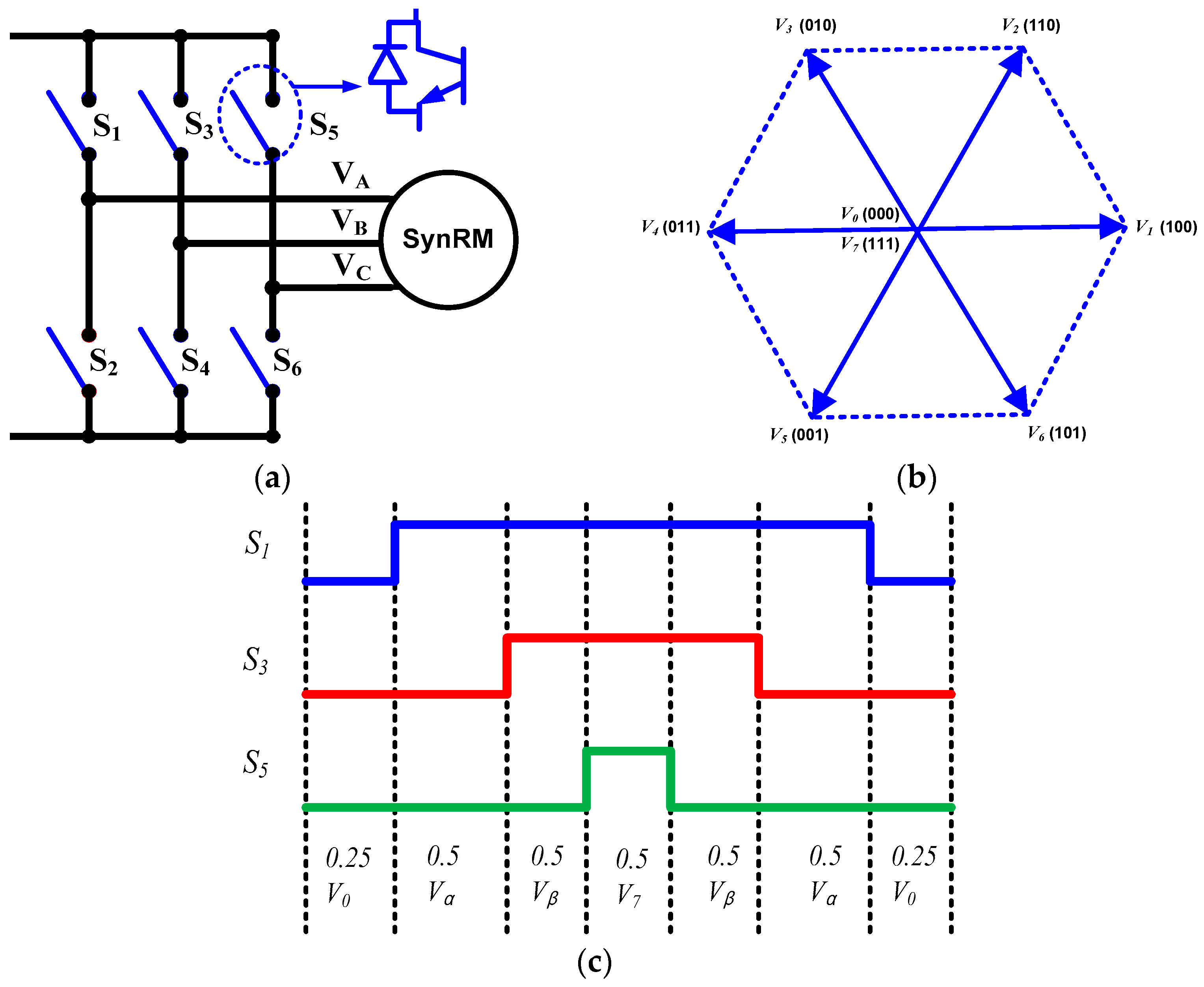
2. Description of the Different SVPWMS
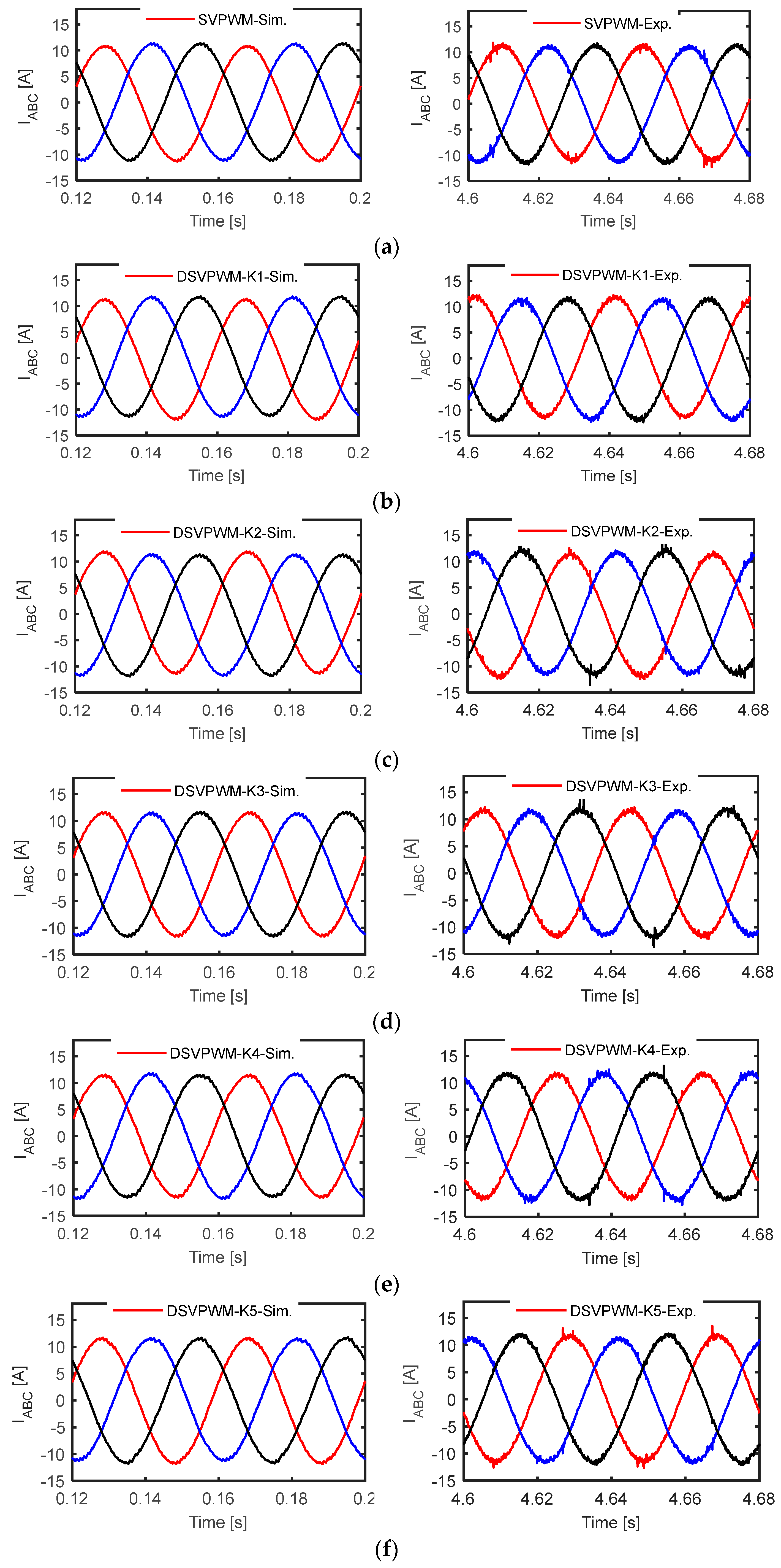
2.1. Continuous SVPWM
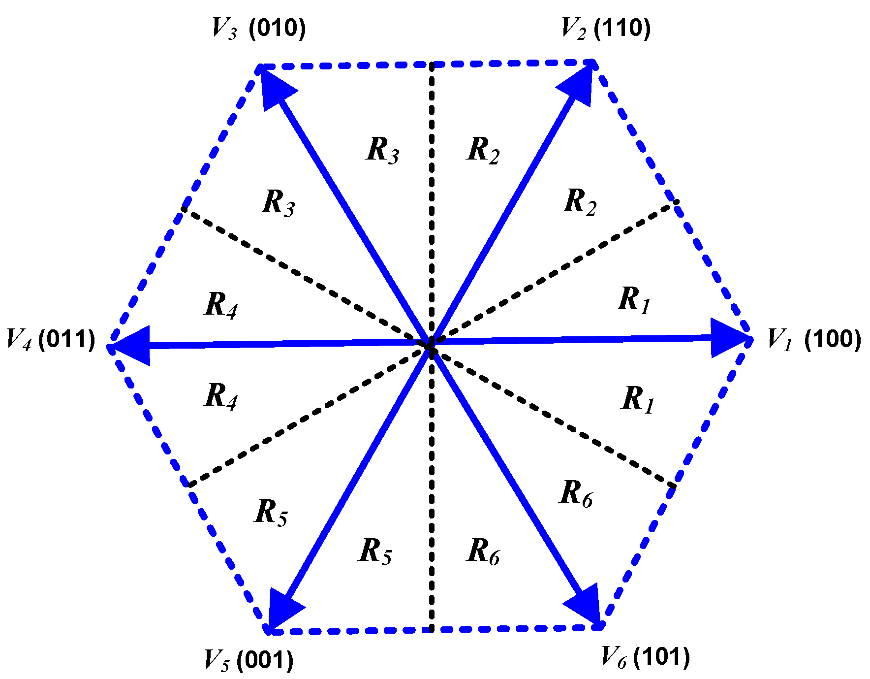
2.2. Discontinuous SVPWMs
2.2.1. DSVPWM-K1
2.2.2. DSVPWM-K2
2.2.3. DSVPWM-K3
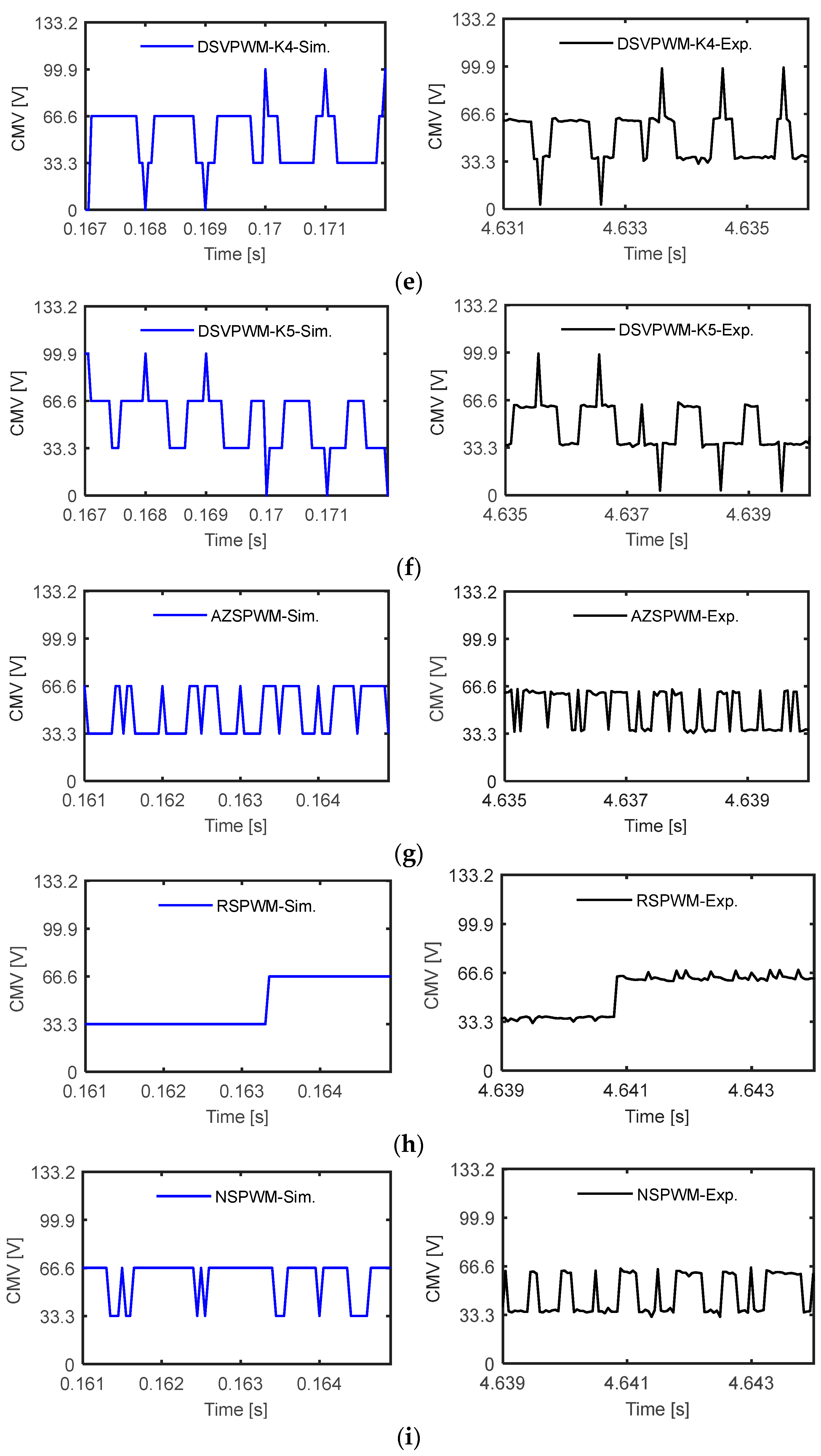
2.2.4. DSVPWM-K4
2.2.5. DSVPWM-K5
2.2.6. AZSPWM
2.2.7. RSPWM
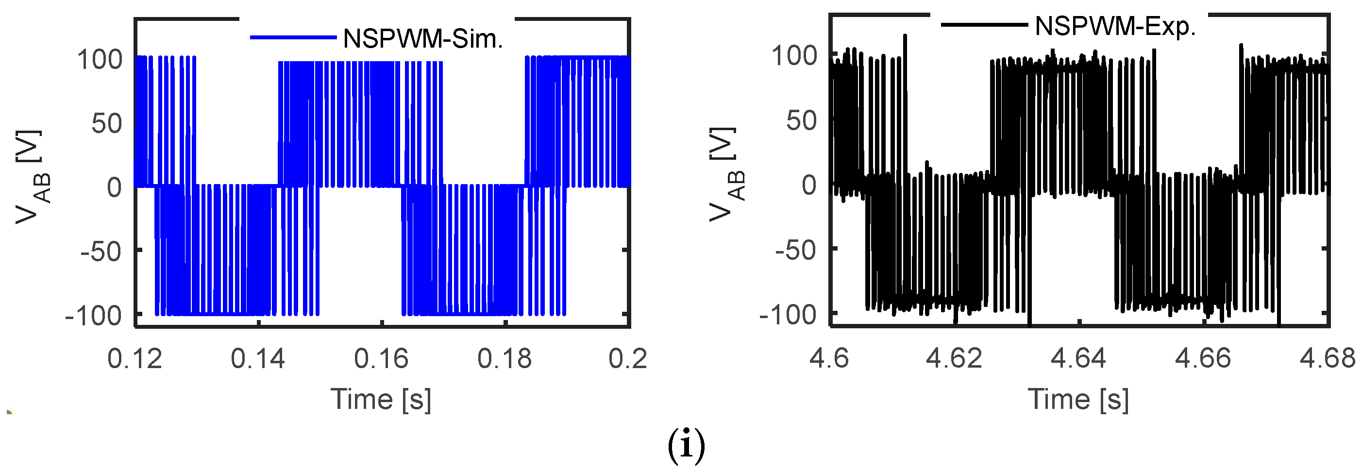
2.2.8. NSPWM
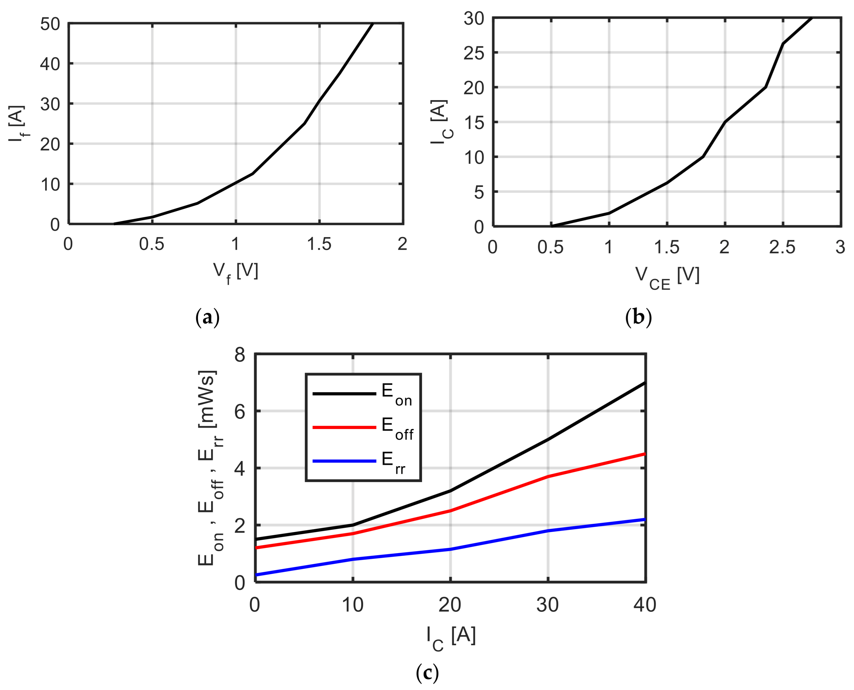
3. Calculation of CMV and Switching and Conduction Losses
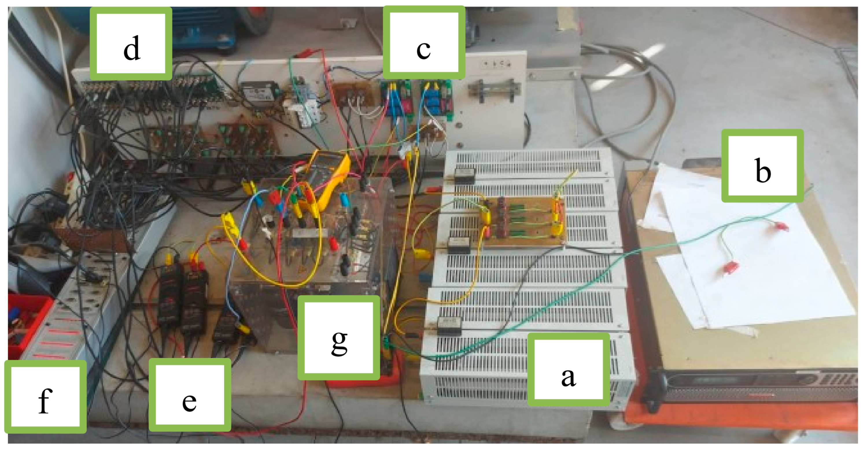
4. Results and Discussion
4.1. CMV Comparison
4.2. Output Voltage Comparison
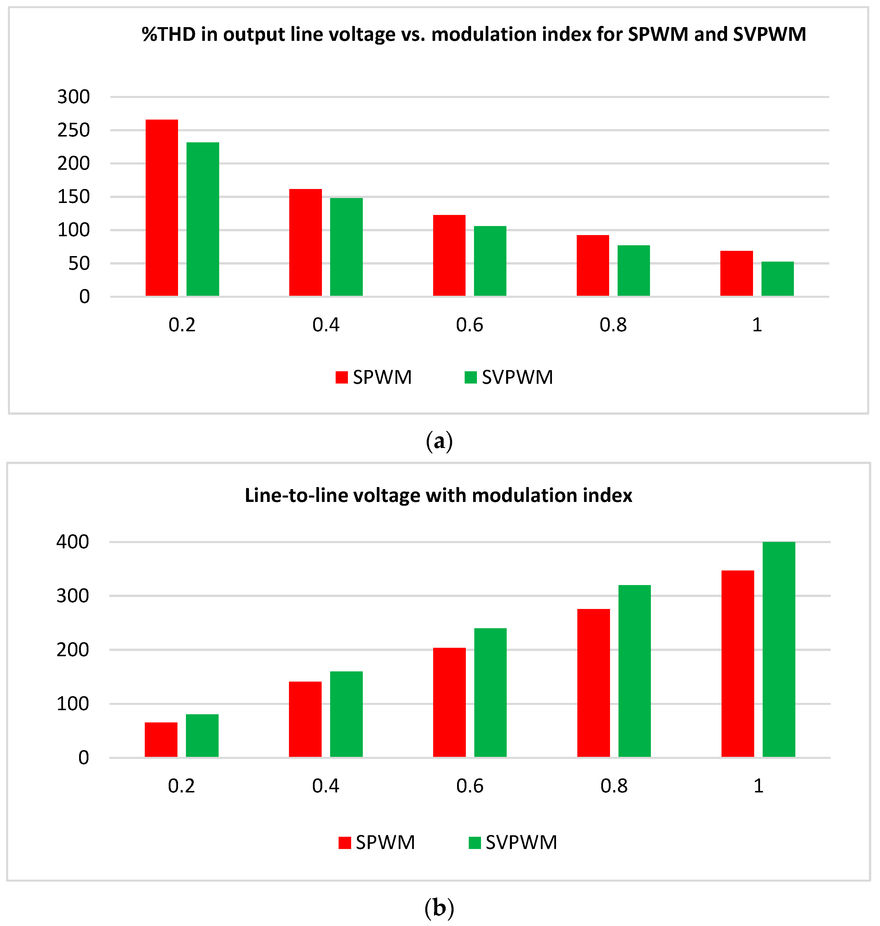
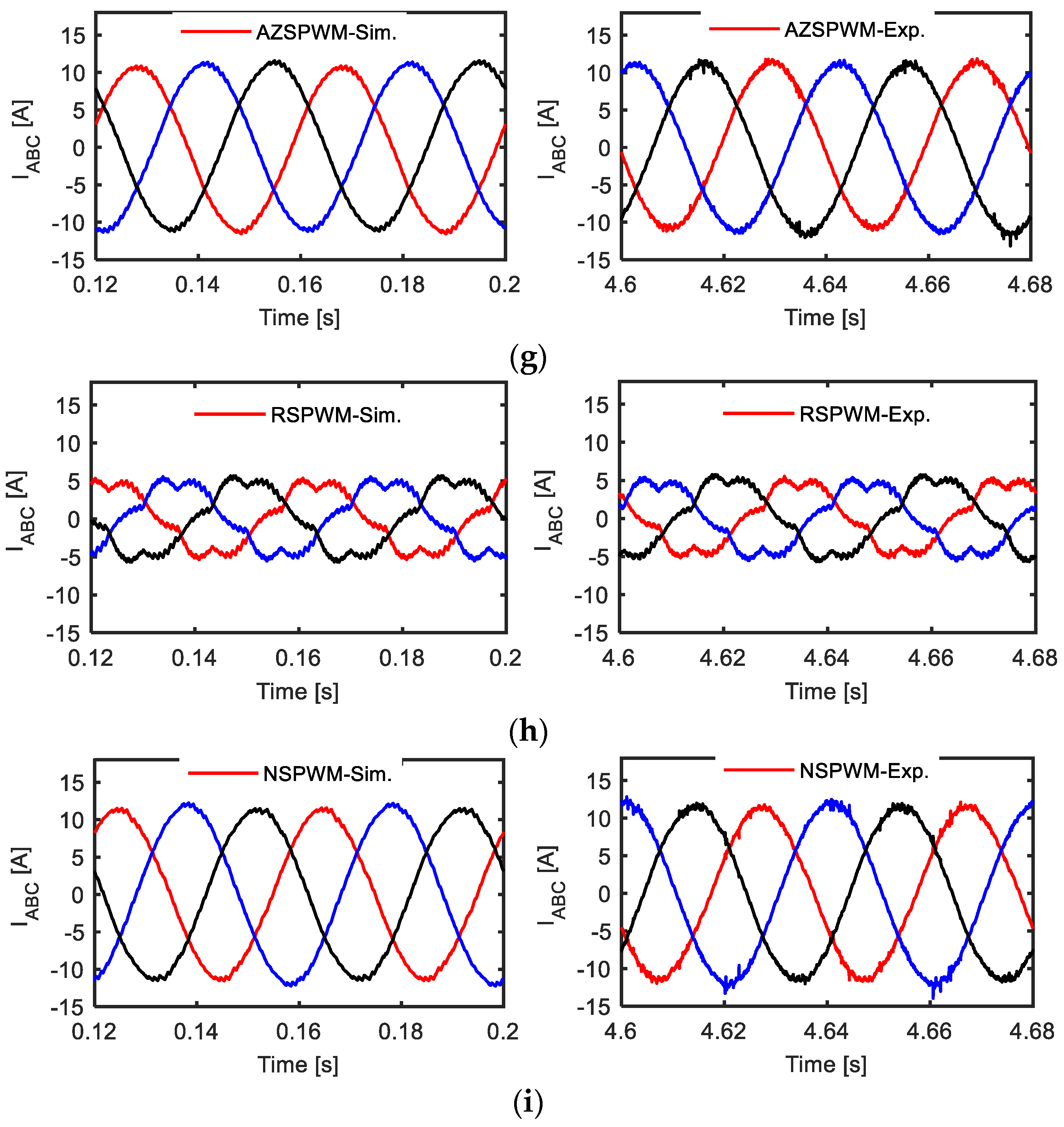
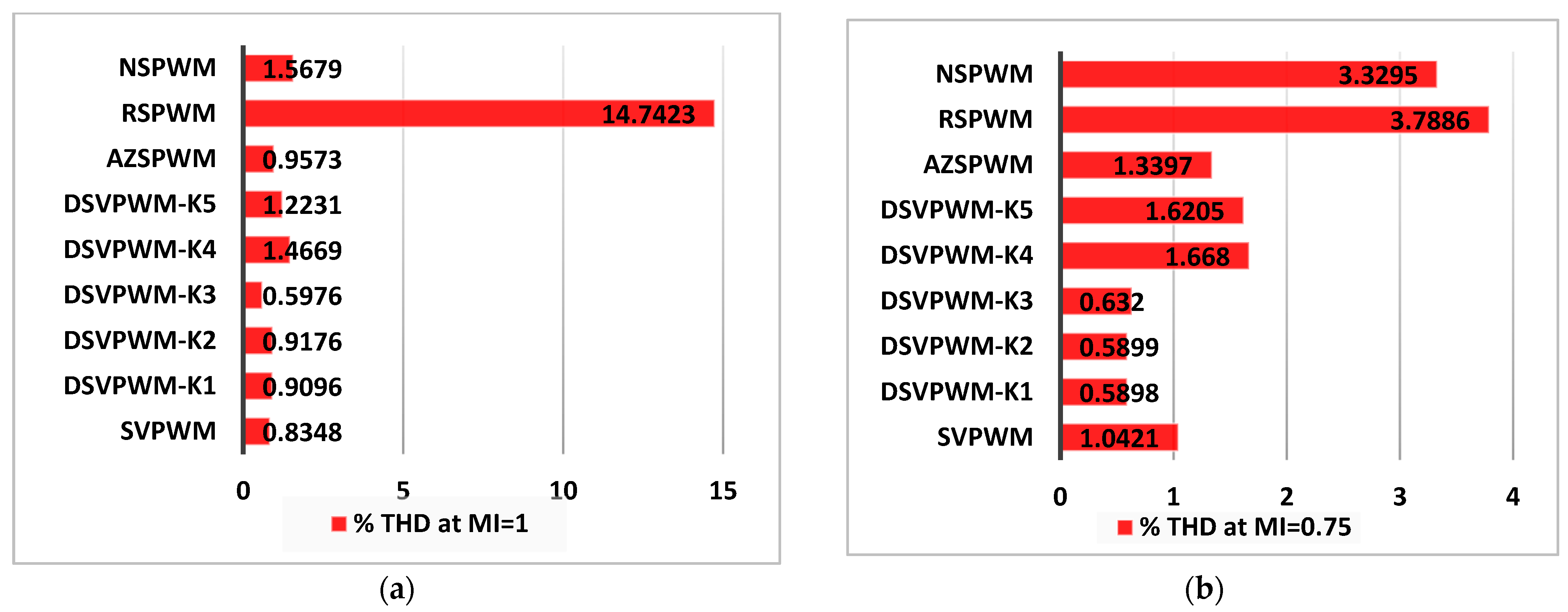
4.3. Output Current and THD Comparison
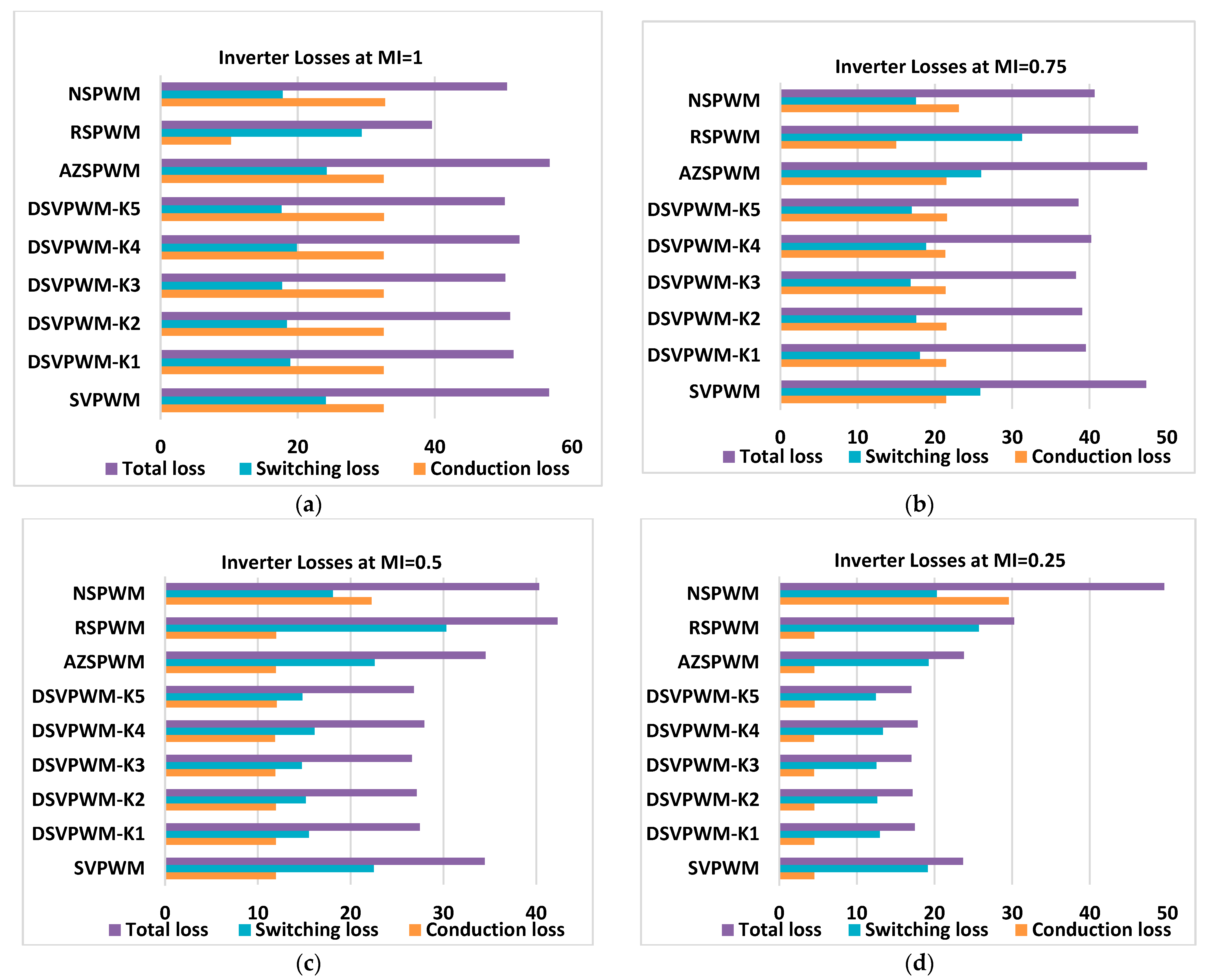
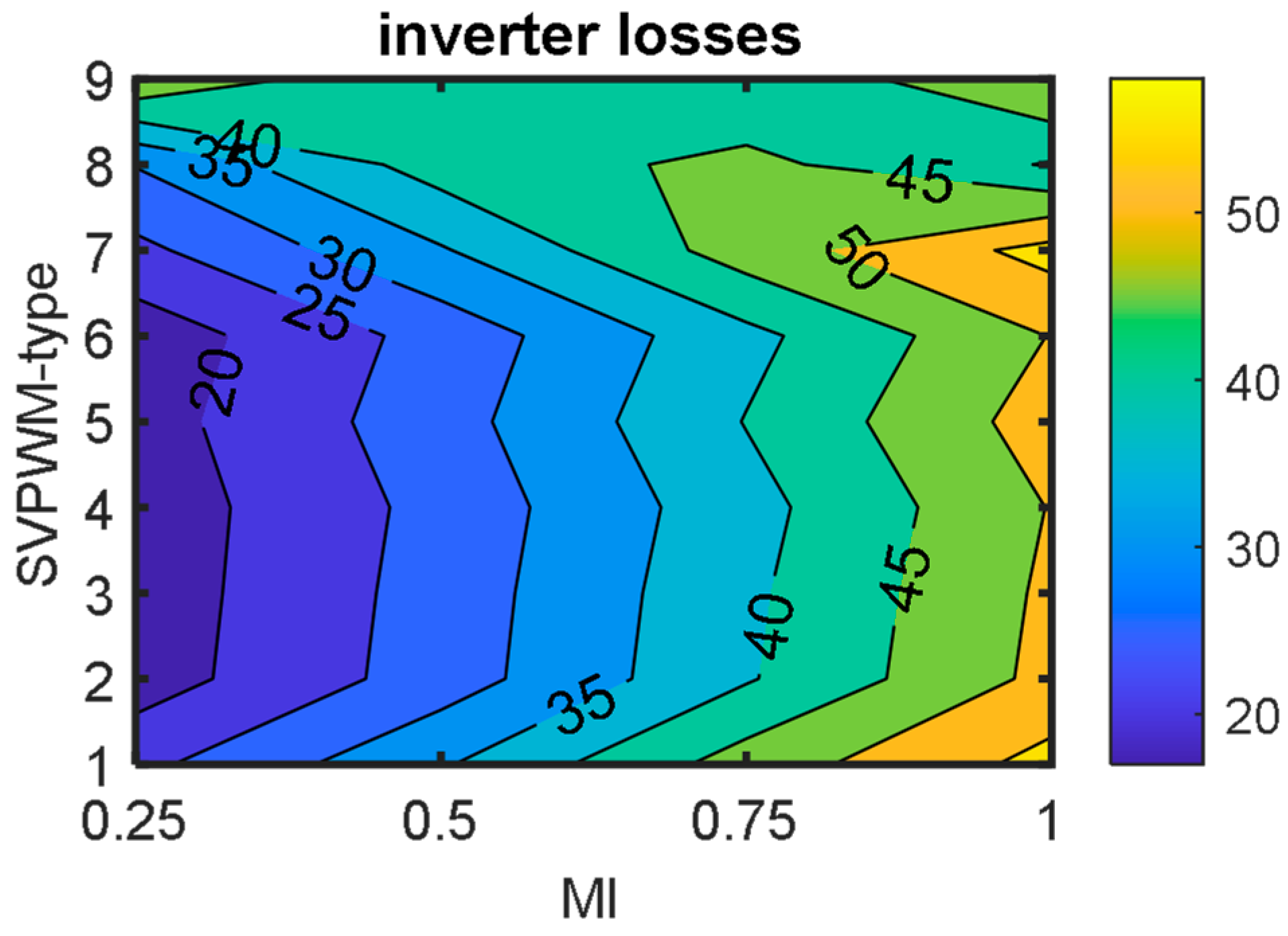
4.4. Inverter Loss Comparison
5. Conclusions
- RSPWM demonstrates the lowest CMV, with a zero peak-to-peak value across different modulation indices. However, RSPWM is only suitable for lower modulation indices (0.25 and 0.5) due to its higher harmonics in the phase currents at higher modulation index values.
- AZSPWM offers optimal performance at high modulation indices (1 and 0.75). It achieves a CMV reduction of 66.66% compared to continuous SVPWM and offers significantly lower THD in the output phase current compared to RSPWM at a high modulation index. RSPWM matches AZSPWM in CMV performance and offers lower inverter losses at high modulation indices. However, NSPWM has nearly double the THD value in the output phase current compared to continuous SVPWM.
- DSVPWM-K1, K2, K3, K4, and K5 offer a 33.33% reduction in CMV compared to continuous SVPWM. These discontinuous SVPWM techniques have shown lower inverter losses compared to SVPWM. Among them, DSVPWM-K3 provides a good compromise by achieving lower inverter losses, a reduced THD of the output phase current, and lower CMV across various modulation indices.
Author Contributions
Funding
Data Availability Statement
Conflicts of Interest
References
- Bakini, H.; Mesbahi, N.; Kermadi, M.; Mekhilef, S.; Zahraoui, Y.; Mubin, M.; Seyedmahmoudian, M.; Stojcevski, A. An Improved Mutated Predictive Control for Two-Level Voltage Source Inverter with Reduced Switching Losses. IEEE Access 2024, 12, 25797–25808. [Google Scholar] [CrossRef]
- Tian, H.; Han, W.; Chen, M.; Liang, G.; Tang, Z. Common-Ground Type Switching Step-Up/Step-Down VSI for Grid-Connected PV System. IEEE Trans. Power Electron. 2024, 39, 10390–10398. [Google Scholar] [CrossRef]
- He, N.; Zhu, Y.; Zhao, A.; Xu, D. Zero-Voltage-Switching Sinusoidal Pulsewidth Modulation Method for Three-Phase Four-Wire Inverter. IEEE Trans. Power Electron. 2019, 34, 7192–7205. [Google Scholar] [CrossRef]
- Huang, J.; Shi, H. Reducing the Common-Mode Voltage through Carrier Peak Position Modulation in an SPWM Three-Phase Inverter. IEEE Trans. Power Electron. 2014, 29, 4490–4495. [Google Scholar] [CrossRef]
- Liang, W.; Wang, J.; Luk, P.C.-K.; Fang, W.; Fei, W. Analytical Modeling of Current Harmonic Components in PMSM Drive with Voltage-Source Inverter by SVPWM Technique. IEEE Trans. Energy Convers. 2014, 29, 673–680. [Google Scholar] [CrossRef]
- Liao, W.; Lyu, M.; Huang, S.; Wen, Y.; Li, M.; Huang, S. An Enhanced SVPWM Strategy Based on Vector Space Decomposition for Dual Three-Phase Machines Fed by Two DC-Source VSIs. IEEE Trans. Power Electron. 2021, 36, 9312–9321. [Google Scholar] [CrossRef]
- Sharma, N.; Garg, V.K. Comparison of SPWM VSI and SVPWM VSI FED Induction Machine Using Volt per Hertz Control Scheme. In Impending Power Demand and Innovative Energy Paths; University Institute of Engineering and Technology: Haryana, India, 2014; ISBN 978-93-83083-84-8. [Google Scholar]
- An, S.-L.; Sun, X.-D.; Zhang, Q.; Zhong, Y.-R.; Ren, B.-Y. Study on the Novel Generalized Discontinuous SVPWM Strategies for Three-Phase Voltage Source Inverters. IEEE Trans. Ind. Inform. 2013, 9, 781–789. [Google Scholar] [CrossRef]
- Samanes, J.; Gubia, E.; Juankorena, X.; Girones, C. Common-Mode and Phase-to-Ground Voltage Reduction in Back-to-Back Power Converters with Discontinuous PWM. IEEE Trans. Ind. Electron. 2020, 67, 7499–7508. [Google Scholar] [CrossRef]
- Haruna, J.O.; Ojo, O. Discontinuous Space Vector Pulse Width Modulation for Six Switch Converter with Independent Control of Phase Voltages and Switching Device Stress Alleviation. IEEE Trans. Ind. Appl. 2023, 59, 4300–4311. [Google Scholar] [CrossRef]
- Lu, H.; Qu, W.; Cheng, X.; Fan, Y.; Zhang, X. A Novel PWM Technique with Two-Phase Modulation. IEEE Trans. Power Electron. 2007, 22, 2403–2409. [Google Scholar] [CrossRef]
- Un, E.; Hava, A.M. A Near-State PWM Method with Reduced Switching Losses and Reduced Common-Mode Voltage for Three-Phase Voltage Source Inverters. IEEE Trans. Ind. Appl. 2009, 45, 782–793. [Google Scholar] [CrossRef]
- Hava, A.M.; Çetin, N.O. A Generalized Scalar PWM Approach with Easy Implementation Features for Three-Phase, Three-Wire Voltage-Source Inverters. IEEE Trans. Power Electron. 2011, 26, 1385–1395. [Google Scholar] [CrossRef]
- Demirkutlu, E.; Hava, A.M. A Scalar Resonant-Filter-Bank-Based Output-Voltage Control Method and a Scalar Minimum-Switching-Loss Discontinuous PWM Method for the Four-Leg-Inverter-Based Three-Phase Four-Wire Power Supply. IEEE Trans. Ind. Appl. 2009, 45, 982–991. [Google Scholar] [CrossRef]
- Li, X.; Deng, Z.; Chen, Z.; Fei, Q. Analysis and Simplification of Three-Dimensional Space Vector PWM for Three-Phase Four-Leg Inverters. IEEE Trans. Ind. Electron. 2011, 58, 450–464. [Google Scholar] [CrossRef]
- Hava, A.M.; Kerkman, R.J.; Lipo, T.A. A high-performance generalized discontinuous PWM algorithm. IEEE Trans. Ind. Appl. 1998, 34, 1059–1071. [Google Scholar] [CrossRef]
- Ojo, O. The generalized discontinuous PWM scheme for three-phase voltage source inverters. IEEE Trans. Ind. Electron. 2004, 51, 1280–1289. [Google Scholar] [CrossRef]
- Reddy, T.B.; Ishwarya, K.; Vyshnavi, D.; Haneesha, K. Generalized scalar PWM algorithm for three-level diode clamped inverter fed induction motor drives with reduced complexity. In Proceedings of the International Conference on Advances in Power Conversion and Energy Technologies (APCET), Mylavaram, India, 2–4 August 2012; pp. 1–6. [Google Scholar] [CrossRef]
- Nguyen, N.-V.; Nguyen, B.-X.; Lee, H.-H. An Optimized Discontinuous PWM Method to Minimize Switching Loss for Multilevel Inverters. IEEE Trans. Ind. Electron. 2011, 58, 3958–3966. [Google Scholar] [CrossRef]
- Lai, Y.-S.; Chen, P.-S.; Lee, H.-K.; Chou, J. Optimal common-mode voltage reduction PWM technique for inverter control with consideration of the dead-time effects-part II: Applications to IM drives with diode front end. IEEE Trans. Ind. Appl. 2004, 40, 1613–1620. [Google Scholar] [CrossRef]
- Cacciato, M.; Consoli, A.; Scarcella, G.; Testa, A. Reduction of common-mode currents in PWM inverter motor drives. IEEE Trans. Ind. Appl. 1999, 35, 469–476. [Google Scholar] [CrossRef]
- Hou, C.-C.; Shih, C.-C.; Cheng, P.-T.; Hava, A.M. Common-Mode Voltage Reduction Pulse Width Modulation Techniques for Three-Phase Grid-Connected Converters. IEEE Trans. Power Electron. 2013, 28, 1971–1979. [Google Scholar] [CrossRef]
- Un, E.; Hava, A.M. A Near State PWM Method with Reduced Switching Frequency and Reduced Common Mode Voltage for Three-Phase Voltage Source Inverters. In Proceedings of the IEEE International Electric Machines & Drives Conference, Antalya, Turkey, 3–5 May 2007; pp. 235–240. [Google Scholar] [CrossRef]
- Hava, A.M.; Ün, E. Performance Analysis of Reduced Common-Mode Voltage PWM Methods and Comparison with Standard PWM Methods for Three-Phase Voltage-Source Inverters. IEEE Trans. Power Electron. 2009, 24, 241–252. [Google Scholar] [CrossRef]
- Amin, A.A.; Tawfiq, K.B.; Youssef, H.; EL-Kholy, E.E. Performance analysis of inverter fed from wind energy system. In Proceedings of the Eighteenth International Middle East Power Systems Conference (MEPCON), Cairo, Egypt, 27–29 December 2016; pp. 512–516. [Google Scholar] [CrossRef]
- Sridevi, C.; Ravikiran, I. Comparative Analysis of SVPWM and DSVPWM Control Techniques for a Single-Phase to Three-Phase Conversion System. Int. J. Sci. Res. 2015, 12, 2506–2512. [Google Scholar]
- Kumar, A.; Chatterjee, D. A survey on space vector pulse width modulation technique for a two-level inverter. In Proceedings of the National Power Electronics Conference (NPEC), Pune, India, 18–20 December 2017; pp. 78–83. [Google Scholar] [CrossRef]
- Zhou, S.; Liu, K.; Hu, W.; Zhang, D.; Huang, C.; Chen, Y. Inverter Harmonic Suppression for Permanent Magnet Synchronous Machine Drives Based on Discontinuous SVPWM with Variable Switching Frequency. IEEE Trans. Transp. Electrif. 2023, 9, 2419–2428. [Google Scholar] [CrossRef]
- Available online: https://www.farnell.com/datasheets/43922.pdf (accessed on 1 June 2023).
- Available online: https://projekter.aau.dk/projekter/files/414361234/PED4_1042_Report.pdf (accessed on 1 June 2023).
- Hu, Z.; Xing, X.; Liu, C.; Zhang, R.; Blaabjerg, F. A Modified Discontinuous PWM Method for Three-Level Inverters with the Improved LCL Filter. IEEE Trans. Power Electron. 2024, 39, 5498–5509. [Google Scholar] [CrossRef]
- Lee, S.-J.; Lee, J.-S.; Lee, K.-B. Novel switching strategy for high-efficiency of single-phase three-level inverters. In Proceedings of the 2014 IEEE Conference on Energy Conversion (CENCON), Johor Bahru, Malaysia, 13–14 October 2014; pp. 342–347. [Google Scholar] [CrossRef]


| Sector | Vα | Vβ | Zero Vectors |
|---|---|---|---|
| 1 | (100) | (110) | (101), (010) |
| 2 | (010) | (110) | (011), (100) |
| 3 | (010) | (011) | (110), (001) |
| 4 | (001) | (011) | (101), (010) |
| 5 | (001) | (101) | (011), (100) |
| 6 | (100) | (101) | (110), (001) |
| Region | Vectors (Vx, Vy, Vz) | Sequence |
|---|---|---|
| R1 | V1, V3, V5 | Vy—Vx—Vz—Vx—Vy |
| R2 | V2, V4, V6 | Vy—Vx—Vz—Vx—Vy |
| R3 | V3, V5, V1 | Vy—Vx—Vz—Vx—Vy |
| R4 | V4, V6, V2 | Vy—Vx—Vz—Vx—Vy |
| R5 | V5, V1, V3 | Vy—Vx—Vz—Vx—Vy |
| R6 | V6, V2, V4 | Vy—Vx—Vz—Vx—Vy |
| Sector | Region | Vectors (Vx, Vy, Vz) | Sequence |
|---|---|---|---|
| 1 | B1 | V1, V2, V6 | Vy—Vx—Vz—Vx—Vy |
| B2 | V2, V1, V3 | Vy—Vx—Vz—Vx—Vy | |
| 2 | B3 | V2, V3, V1 | Vy—Vx—Vz—Vx—Vy |
| B4 | V3, V2, V4 | Vy—Vx—Vz—Vx—Vy | |
| 3 | B5 | V3, V4, V2 | Vy—Vx—Vz—Vx—Vy |
| B6 | V4, V3, V5 | Vy—Vx—Vz—Vx—Vy | |
| 4 | B7 | V4, V5, V3 | Vy—Vx—Vz—Vx—Vy |
| B8 | V5, V4, V6 | Vy—Vx—Vz—Vx—Vy | |
| 5 | B9 | V5, V6, V4 | Vy—Vx—Vz—Vx—Vy |
| B10 | V6, V5, V1 | Vy—Vx—Vz—Vx—Vy | |
| 6 | B11 | V6, V1, V5 | Vy—Vx—Vz—Vx—Vy |
| B12 | V1, V6, V2 | Vy—Vx—Vz—Vx—Vy |
| DC Voltage | 100 V | Output Frequency | 25 Hz |
| Load Resistance | 1.5 Ω | Load Inductance | 0.03 H |
| Sampling Frequency | 20 kHz | DC-Link Capacitor | 4700 µF |
Disclaimer/Publisher’s Note: The statements, opinions and data contained in all publications are solely those of the individual author(s) and contributor(s) and not of MDPI and/or the editor(s). MDPI and/or the editor(s) disclaim responsibility for any injury to people or property resulting from any ideas, methods, instructions or products referred to in the content. |
© 2024 by the authors. Licensee MDPI, Basel, Switzerland. This article is an open access article distributed under the terms and conditions of the Creative Commons Attribution (CC BY) license (https://creativecommons.org/licenses/by/4.0/).
Share and Cite
Tawfiq, K.B.; Sergeant, P.; Mansour, A.S. Comparative Analysis of Space Vector Pulse-Width Modulation Techniques of Three-Phase Inverter to Minimize Common Mode Voltage and/or Switching Losses. Mathematics 2024, 12, 2832. https://doi.org/10.3390/math12182832
Tawfiq KB, Sergeant P, Mansour AS. Comparative Analysis of Space Vector Pulse-Width Modulation Techniques of Three-Phase Inverter to Minimize Common Mode Voltage and/or Switching Losses. Mathematics. 2024; 12(18):2832. https://doi.org/10.3390/math12182832
Chicago/Turabian StyleTawfiq, Kotb B., Peter Sergeant, and Arafa S. Mansour. 2024. "Comparative Analysis of Space Vector Pulse-Width Modulation Techniques of Three-Phase Inverter to Minimize Common Mode Voltage and/or Switching Losses" Mathematics 12, no. 18: 2832. https://doi.org/10.3390/math12182832
APA StyleTawfiq, K. B., Sergeant, P., & Mansour, A. S. (2024). Comparative Analysis of Space Vector Pulse-Width Modulation Techniques of Three-Phase Inverter to Minimize Common Mode Voltage and/or Switching Losses. Mathematics, 12(18), 2832. https://doi.org/10.3390/math12182832