Article

Analysis of an Interface Crack between Piezoelectric Semiconductor Coating and Elastic Substrate Structure

School of Mathematical and Statistics, Ningxia University, Yinchuan 750021, China
*
Authors to whom correspondence should be addressed.
Mathematics 2024, 12(8), 1208; https://doi.org/10.3390/math12081208
Submission received: 11 March 2024 / Revised: 3 April 2024 / Accepted: 9 April 2024 / Published: 17 April 2024
(This article belongs to the Special Issue Mathematical Applications in Electrical Engineering)

Abstract

:
Piezoelectric semiconductor materials possess a unique combination of piezoelectric and semiconductor effects, exhibiting multifaceted coupling properties such as electromechanical, acoustic, photoelectric, photovoltaic, thermal, and thermoelectric capabilities. This study delves into the anti-plane mechanical model of an interface crack between a strip of piezoelectric semiconductor material and an elastic material. By introducing two boundary conditions, the mixed boundary value problem is reformulated into a set of singular integral equations with a Cauchy kernel. The details of carrier concentration, current density, and electric displacement near the crack are provided in a numerical analysis. The findings reveal that the distribution of the current density, carrier concentration, and electric displacement is intricately influenced by the doping concentration of the piezoelectric semiconductor. Moreover, the presence of mechanical and electric loads can either expedite or decelerate the growth of the crack, highlighting the pivotal role of external stimuli in influencing material behavior.

1. Introduction

Piezoelectric semiconductor (PSC) devices, such as elemental crystal selenium, tellurium, doped BaTiO3, and some lead series piezoelectric ceramics, have been favored by researchers because of their combined piezoelectric and semiconductor characteristics [1,2]. Due to the development of epitaxial single crystal layer transducers and thin-film transducers, PSCs, such as zinc oxide (ZnO), cadmium sulfide (CdS), and other compounds, can use vacuum evaporation or sputtering technology to form very thin coatings [3,4,5,6,7]. However, these structures inevitably produce cracks and other defects inside the coating or at the interface junction during the manufacturing process, which will reduce the reliability of the device and shorten the service life of the device under the action of loads [8].
Many scholars have theoretically analyzed the fracture mechanics behavior of PSCs. The mechanical behavior of cracks or holes in PSCs under anti-plane shear force and uniform electrical loads were investigated in Refs. [9,10,11]. Fan et al. [12] proposed an iterative method for calculating the intensity field and current of PSCs, realizing a mechanical analysis of cracked PSC plates using the finite element method. Qin et al. [13] studied the fracture behavior of GaN PSC ceramics under combined mechanical and electrical loads by using the three-point bending test and a numerical analysis. In Refs. [14,15,16], the two-dimensional and three-dimensional crack problems of PSCs were further considered by using an iterative method. Using standard integral transformation and singular integral equation techniques, Zhao et al. [17] analyzed the transient response of mode III cracks in PSC materials under anti-plane shear mechanical and in-plane electrical combined shocks. Sladek et al. [18,19] provided numerical analysis results for crack problems in PSCs under dynamic and transient thermal loads. Generalized boundary conditions and sample geometry were considered in the study, and the coupling control partial differential equations of stress, electric field and current were demonstrated in a locally weak form in a small virtual subdomain.
As a typical structural element, coating substrate systems are widely used in various types of engineering equipment [20,21,22]. Using linear piezoelectric theory, Kwon and Lee [23] obtained a semi-analytical solution for the interface crack problem between piezoelectric ceramics and an elastic material. The problem was simplified into a pair of dual integral equations by Fourier transform and numerically solved. Based on the Stroh complex potential theory and an impermeable crack model, Ou and Chen [24] studied the problem of interface cracks in elastic/piezoelectric bi-materials. The numerical results of the near-end stress and electric fields of 35 dissimilar bi-materials composed of five elastic dielectric materials and seven piezoelectric ceramics were presented. In Refs. [25,26], an extended finite element method and meshless method based on the local Petrov–Galerkin method were proposed to analyze the interface cracks problem between piezoelectric materials. The mechanical behavior of fine-grained piezoelectric/substrate structures with spiral dislocations and interface edge cracks under multi field coupling were studied in [27]. The interface crack model with a contact zone at the crack tip was established and transformed into a Dirichlet and Riemann boundary value problem to obtain a solution [28,29]. A simple equation and a closed analytical formula for determining the actual length of the contact zone were derived. Taking into account the micro-crack damage situation of the material, a new piezoelectric thin-film interface model was developed to characterize the damage behavior of the interface by Rizzoni et al. [30]. The dynamic behavior of elastic laminates with interface delamination and interaction surfaces was simulated using the boundary integral equation method [31]. Furthermore, the transient response of a piezoelectric interface crack under a mechanical impact and the problem of moving interface cracks [32,33], interface multiple cracks [34,35,36], and inhomogeneous piezoelectric interface cracks [37,38] were studied.
Different to traditional piezoelectric materials, PSC structures have unique characteristics of electromechanical carrier multi-field coupling. In the practical application of PSC devices and components, the interface characteristics play a leading role in the reliability and performance of the system [39,40,41]. For PSC composite structures, debonding or interfacial fractures between two adjacent layers are a typical failure mechanism. To the authors’ best knowledge, there is no report on the study of interface cracks in the substrate structures of PSC coatings. The purpose of this paper is to establish a finite domain interface crack problem model for piezoelectric semiconductors, and to transform complex mixed boundary value problems into singular integral equation solutions. Different mechanical and electrical loads were used to conduct a more in-depth study of the fracture behavior of the piezoelectric semiconductor material.
In this paper, an analysis model of the interface crack of the elastic substrate structure of PSC coating is established, two boundary conditions are given, and the expressions of displacement, potential, and carrier components are obtained by Fourier transform. By introducing new unknown functions, the mixed boundary value problem is transformed into a system of singular integral equations with a Cauchy kernel for the solution. Variations in the interface crack intensity factor and energy release rate under two boundary conditions are discussed in detail.

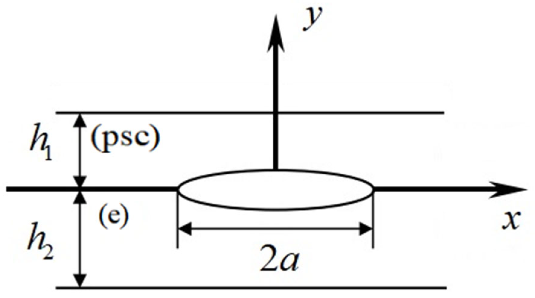
2. Description of the Problem

As shown in Figure 1, an interface crack with a length of 2a exists at the interface between the PSC strip with a thickness of h1 and the elastic strip with a thickness of h2, where the xoy plane is the isogenous plane and the polarization direction of the PSC is the z axis. The Cartesian coordinate system is used here, and the upper and lower surfaces of the structure are subjected to loads. Due to the symmetry of the problem, only the part where x ≥ 0 is considered.
The electric field intensity, electron density and current intensity within the plate are represented by E i , n , J i respectively. According to the equilibrium equation of the force, the Gaussian theorem, and the charge conservation, one can obtain [41,42]:
σ i j , j ( psc ) = 0 , D i , i = q n , J i , i = 0 , σ i j , j ( e ) = 0 ,
where σ i j , D i , q represent the stress tensor, electrical shift, and electronic charge, respectively. The superscript (psc) and (e) denote the PSC and elastic layers, respectively. Here, i, j = 1, 2, 3, and the “j” after the comma in the subscript means that the derivative of the corresponding coordinate direction will be taken. According to the piezoelectric theory and the semiconductor theory, the constitutive relationship of the n-type PSC is [43,44]:
σ 13 ( psc ) = c 44 ( psc ) u 3 / x + e 15 ϕ / x , σ 23 ( psc ) = c 44 ( psc ) u 3 / y + e 15 ϕ / y , D 1 = e 15 u 3 / x ε 11 ϕ / x , D 2 = e 15 u 3 / y ε 11 ϕ / y , J 1 = q n 0 μ 11 ϕ / x + q d 11 n / x , J 2 = q n 0 μ 11 ϕ / y + q d 11 n / y . σ 23 ( e ) = c 44 ( e ) u 3 / y ,
where c 44 , e 15 , ε 11 represent the elastic constant, piezoelectric constant, and dielectric constant, and d 11 , μ 11 are the diffusion coefficient and mobility of the electrons. Here, u i represents the displacement vector and ϕ represents the potential function.
Substituting Equation (2) into (1) yields:
c 44 ( psc ) 2 u 3 ( psc ) + e 15 2 ϕ = 0 , e 15 2 u 3 ( psc ) ε 11 2 ϕ = q n , n 0 μ 11 2 ϕ + d 11 2 n = 0 , c 44 ( e ) 2 u 3 ( e ) = 0 ,
where 2 = 2 x 2 + 2 y 2 is the two-dimensional Laplace operator, with Equation (3) deformable as:
2 n = μ 11 c 44 ( psc ) q n 0 d 11 e 15 2 + c 44 ( psc ) ε 11 n , 2 u 3 ( psc ) = e 15 q e 15 2 + c 44 ( psc ) ε 11 n , 2 ϕ = c 44 ( psc ) q e 15 2 + c 44 ( psc ) ε 11 n , u 3 ( e ) = 0 .

3. Boundary Conditions

This paper considers two boundary conditions, as follows.
For the anti-plane problem, one obtains:
u 1 ( psc ) ( x , y ) = u 2 ( psc ) ( x , y ) = 0 , u 3 ( psc ) = u 3 ( psc ) ( x , y ) ,   ϕ = ϕ ( x , y ) ,   n = n ( x , y ) , u 1 ( e ) ( x , y ) = u 2 ( e ) ( x , y ) = 0 ,   u 3 ( e ) = u 3 ( e ) ( x , y ) .
The following boundary conditions are considered:
σ 23 ( psc ) ( x , 0 + ) = σ 23 ( e ) ( x , 0 ) = 0 , ( x < a ) , u 3 ( psc ) ( x , 0 ) = u 3 ( e ) ( x , 0 ) , ( x a ) , σ 23 ( psc ) ( x , 0 ) = σ 23 ( e ) ( x , 0 ) , ( x a ) , u 3 ( psc ) x , 0 = 0 , ϕ x , 0 = 0 , n x , 0 = 0 , ( | x | > a ) ,
c a s e   1 σ 23 ( e ) ( x , h 2 ) = σ 23 ( psc ) ( x , h 1 ) = p ( x ) , D 2 ( psc ) ( x , h 1 ) = 0 , J 2 ( psc ) ( x , h 1 ) = J ( x ) , D 2 ( psc ) ( x , 0 ) = 0 , J 2 ( psc ) ( x , 0 ) = 0 , ( x < ) ,
c a s e   2 σ 23 ( e ) ( x , h 2 ) = σ 23 ( psc ) ( x , h 1 ) = p ( x ) , D 2 ( psc ) ( x , h 1 ) = D ( x ) , J 2 ( psc ) ( x , h 1 ) = 0 , D 2 ( psc ) ( x , 0 ) = 0 , J 2 ( psc ) ( x , 0 ) = 0 , ( x < ) .

4. Theoretical Analysis and Solution

First, we consider case 1. In order to solve the problem, (4) can be written as:
2 n β 2 n = 0 , β 2 = μ 11 c 44 ( psc ) q n 0 d 11 e 15 2 + c 44 ( psc ) ε 11 .
Since the crack is symmetrical concerning x = 0, the region of x > 0, y > 0 can be considered. The Fourier cosine transformation of Equation (9) results in:
d 2 n ˜   d y 2 s 2 + β 2 n ˜ = 0 , n ˜ s , y = 0 n x , y cos ( s x ) d x , n x , y = 2 π 0 n ˜ s , y cos ( s x ) d s .
Take s 2 + β 2 = ω 2 and assume that ω > 0 , Equation (10) can be written as
n ˜ s , y = A ( s ) e ω y + B ( s ) e ω y .
Then,
n x , y = 2 π 0 A ( s ) e ω y + B ( s ) e ω y cos ( s x ) d s .
In the same way,
u 3 ( psc ) x , y = 2 π 0 C 1 ( s ) e s y + C 2 ( s ) e s y e 15 d 11 c 44 μ 11 n 0 A ( s ) e ω y e 15 d 11 c 44 μ 11 n 0 B ( s ) e ω y cos s x d s ,
u 3 ( e ) ( x , y ) = 2 π 0 [ D 1 ( s ) e s y + D 2 ( s ) e s y ] cos s x d s ,
ϕ ( x , y ) = 2 π 0 E 1 ( s ) e s y + E 2 ( s ) e s y + d 11 μ 11 n 0 A ( s ) e ω y + B ( s ) e ω y cos ( s x ) d s .
Substituting Equations (12)–(15) into (2) yields:
σ 23 ( e ) ( x , y ) = 2 π 0 c 44 ( e ) s D 1 ( s ) e s y + s D 2 ( s ) e s y cos s x d s ,
σ 23 ( psc ) ( x , y ) = 2 π 0 s c 44 ( psc ) C 1 ( s ) e s y + C 2 ( s ) e s y + e 15 E 1 ( s ) e s y + E 2 ( s ) e s y cos s x d s ,
D 2 ( x , y ) = 2 π 0 e 15 s C 1 ( s ) e s y + s C 2 ( s ) e s y ε 11 s E 1 ( s ) e s y + s E 2 ( s ) e s y cos ( s x ) d s + 2 π 0 q β 2 ω A ( s ) e ω y B ( s ) e ω y cos ( s x ) d s ,
J 2 ( x , y ) = q n 0 μ 11 2 π 0 s E 1 ( s ) e s y + s E 2 ( s ) e s y cos ( s x ) d s .
To obtain the solution, the following three dislocation density functions are introduced:
g 1 ( x ) = n x ( x , 0 ) = 2 π 0 s A ( s ) + B ( s ) sin s x d s , g 2 ( x ) = u 3 ( psc ) x ( x , 0 ) u 3 ( e ) x ( x , 0 ) , = s 2 π 0 a C 1 ( s ) + C 2 ( s ) e 15 d 11 c 44 ( psc ) μ 11 n 0 A ( s ) + B ( s ) D 1 ( s ) + D 2 ( s ) sin s x d s , g 3 ( x ) = ϕ x ( x , 0 ) = 2 π 0 s E 1 ( s ) + E 2 ( s ) + d 11 μ 11 n 0 A ( s ) + d 11 μ 11 n 0 B ( s ) sin s x d s .
Performing the sine transform on (20) and substituting Equation (6) into Equations (16), (18) and (19), unknown functions A(s), B(s), C1(s), C2(s), E1(s), E2(s) D1(s), D2(s) will be determined. Substituting Equation (7) into Equations (16), (18) and (19) yields:
σ 23 ( e ) ( x , y ) = 2 π 0 [ s D 1 ( s ) + s D 2 ( s ) ] cos s x d s = p ( x ) c 44 ( e ) , D 2 ( x , y ) = 2 π 0 ω [ A ( s ) B ( s ) ] cos ( s x ) d s = J ( x ) ε 11 c 44 ( psc ) p ( x ) e 15 q n 0 μ 11 + J ( x ) e 15 2 q d 11 ( e 15 2 + ε 11 c 44 ( psc ) ) , J 2 ( x , y ) = 2 π 0 s E 1 ( s ) + s E 2 ( s ) cos s x d s = J ( x ) q n 0 μ 11 .
A(s), B(s), C1(s), C2(s), E1(s), E2(s) D1(s), D2(s) are substituted into Equation (21) to obtain the following system of singular integral equations:
1 π a a g 3 ( r ) + c 44 ( psc ) g 2 ( r ) 0 2 e 2 s h 1 e 2 s h 1 e 2 s h 2 1 + e 2 s h 2 ( e 2 s h 1 e 2 s h 2 1 ) + c 44 ( e ) c 44 ( psc ) c 44 ( e ) + c 44 ( psc ) ( e 2 s h 2 e 2 s h 1 ) sin ( s r ) cos ( s x ) d r d s = p ( x ) ( c 44 ( e ) + c 44 ( psc ) ) c 44 ( e ) , 1 π a a g 1 ( r ) 0 2 ω ( 1 e 2 ω h 1 ) s ( 1 + e 2 ω h 1 ) sin ( s r ) cos ( s x ) d r d s = J ( x ) ε 11 c 44 ( psc ) p ( x ) e 15 q n 0 μ 11 + J ( x ) e 15 2 q d 11 ( e 15 2 + ε 11 c 44 ( psc ) ) , 1 π a a g 3 ( r ) d 11 μ 11 n 0 g 1 ( r ) 0 2 ( 1 e 2 s h 1 ) ( 1 + e 2 s h 1 ) sin ( s r ) cos ( s x ) d r d s = J ( x ) q n 0 μ 11 .
The singularity of the above equations is separated to obtain:
1 π a a g 3 ( r ) + c 44 ( psc ) g 2 ( r ) R 3 ( x , r ) 1 r x d r = p ( x ) ( c 44 ( e ) + c 44 ( psc ) ) c 44 ( e ) , 1 π a a g 1 ( r ) R 2 ( x , r ) 1 r x d r = J ( x ) ε 11 c 44 ( psc ) p ( x ) e 15 q n 0 μ 11 + J ( x ) e 15 2 q d 11 ( e 15 2 + ε 11 c 44 ( psc ) ) , 1 π a a g 3 ( r ) d 11 μ 11 n 0 g 1 ( r ) R 1 ( x , r ) 1 r x d r = J ( x ) q n 0 μ 11 ,
where
R 1 ( x , r ) = 0 2 ( 1 e 2 s h 1 ) ( 1 + e 2 s h 1 ) 2 sin ( s r ) cos ( s x ) d s + 1 r + x , R 2 ( x , r ) = 0 2 ω ( 1 e 2 ω h 1 ) s ( 1 + e 2 ω h 1 ) 2 sin ( s r ) cos ( s x ) d s + 1 r + x , R 3 ( x , r ) = 0 2 e 2 s h 1 e 2 s h 1 e 2 s h 2 1 + e 2 s h 2 ( e 2 s h 1 e 2 s h 2 1 ) + c 44 ( e ) c 44 ( psc ) c 44 ( e ) + c 44 ( psc ) ( e 2 s h 2 e 2 s h 1 ) 2 sin ( s r ) cos ( s x ) d s + 1 r + x .
For Equation (23), changing the integration interval to [−1, 1] results in:
1 π 1 1 c 44 ( psc ) f 2 ( r ¯ ) + f 3 ( r ¯ ) R 3 ( x ¯ , r ¯ ) + 1 r ¯ + x ¯ 1 r ¯ x ¯ d r ¯ = p ( x ¯ ) ( c 44 ( e ) + c 44 ( psc ) ) c 44 ( e ) , 1 π 1 1 f 1 ( r ¯ ) 1 r ¯ x ¯ + R 2 ( x ¯ , r ¯ ) d r ¯ = J ( x ¯ ) ε 11 c 44 ( psc ) p ( x ¯ ) e 15 q n 0 μ 11 + J ( x ¯ ) e 15 2 q d 11 ( e 15 2 + ε 11 c 44 ( psc ) ) , 1 π 1 1 f 3 ( r ¯ ) d 11 μ 11 n 0 f 1 ( r ¯ ) 1 r ¯ x ¯ + R 1 ( x ¯ , r ¯ ) d r ¯ = J ( x ¯ ) q n 0 μ 11 ,
where
x = a x ¯ , r = a r ¯ , f 1 ( r ¯ ) = g 1 ( r ) , f 2 ( r ¯ ) = g 2 ( r ) , f 3 ( r ¯ ) = g 3 ( r ) , f 1 ( r ¯ ) = F 1 ( r ¯ ) ( 1 + r ¯ ) ( 1 r ¯ ) , f 2 ( r ¯ ) = F 2 ( r ¯ ) ( 1 + r ¯ ) ( 1 r ¯ ) , f 3 ( r ¯ ) = F 3 ( r ¯ ) ( 1 + r ¯ ) ( 1 r ¯ ) , 1 1 f 1 ( r ¯ ) d r ¯ = 1 1 f 2 ( r ¯ ) d r ¯ = 1 1 f 3 ( r ¯ ) d r ¯ = 0 .
Equation (25) is discretized into the following algebraic equation systems:
1 N k = 1 N c 44 ( psc ) F 2 r k 1 r k x t + π R 3 a x t , a r k + 1 N k = 1 N F 3 r k 1 r k x t + π R 3 a x t , a r k = p ( x t ) ( c 44 ( e ) + c 44 ( psc ) ) c 44 ( e ) , k = 1 N 1 N F 1 r k 1 r k x t + π R 2 a x t , a r k = J ( x t ) ε 11 c 44 ( psc ) p ( x t ) e 15 q n 0 μ 11 + J ( x t ) e 15 2 q d 11 ( e 15 2 + ε 11 c 44 ( psc ) ) , 1 N k = 1 N F 3 r k 1 r k x t + π R 1 a x t , a r k + d 11 μ 11 n 0 1 N k = 1 N F 1 r k 1 r k x t + π R 1 a x t , a r k = J ( x t ) q n 0 μ 11 , k = 1 N π N F 1 r k = 0 , k = 1 N π N F 2 r k = 0 , k = 1 N π N F 3 r k = 0 ,
where
r k = cos ( 2 k 1 ) 2 N π ,   k = 1 ,   2 ,   ,   N ;   x t = cos t N π ,   t = 1 ,   2 , ,   N 1 .
Next, we will consider case 2.
Considering the boundary conditions, the following equations can be obtained through σ 23 , D 2 , J 2 at the crack surface:
2 π 0 s D 1 ( s ) + s D 2 ( s ) cos s x d s = p ( x ) c 44 ( e ) , 2 π 0 ω A ( s ) B ( s ) cos ( s x ) d s = μ 11 n 0 [ c 44 ( psc ) D ( x ) p ( x ) e 15 ] d 11 ( e 15 2 + c 44 ( psc ) ε 11 ) , 2 π 0 s E 1 ( s ) + s E 2 ( s ) cos s x d s = 0 .
A(s), B(s), C1(s), C2(s), E1(s), E2(s) D1(s), D2(s) into Equation (29) can be substituted to obtain the following singular integral equation system:
1 π a a g 3 ( r ) + c 44 ( psc ) g 2 ( r ) T 3 ( x , r ) 1 r x d r = p ( x ) ( c 44 ( e ) + c 44 ( psc ) ) c 44 ( e ) , 1 π a a g 1 ( r ) T 2 ( x , r ) 1 r x d r = μ 11 n 0 c 44 ( psc ) D ( x ) p ( x ) e 15 d 11 ( e 15 e 15 + c 44 ( psc ) ε 11 ) , 1 π a a g 3 ( r ) d 11 μ 11 n 0 g 1 ( r ) T 1 ( x , r ) 1 r x d r = 0 ,
where
T 1 ( x , r ) = 0 2 ( 1 e 2 s h 1 ) ( 1 + e 2 s h 1 ) 2 sin ( s r ) cos ( s x ) d s + 1 r + x , T 2 ( x , r ) = 0 2 ω ( 1 e 2 ω h 1 ) s ( 1 + e 2 ω h 1 ) 2 sin ( s r ) cos ( s x ) d s + 1 r + x , T 3 ( x , r ) = 0 2 e 2 s h 1 e 2 s h 1 e 2 s h 2 1 + e 2 s h 2 ( e 2 s h 1 e 2 s h 2 1 ) + c 44 ( e ) c 44 ( psc ) c 44 ( e ) + c 44 ( psc ) ( e 2 s h 2 e 2 s h 1 ) 2 sin ( s r ) cos ( s x ) d s + 1 r + x .
Equation (30) is normalized as:
1 π 1 1 c 44 ( psc ) f 2 ( r ¯ ) + f 3 ( r ¯ ) T 3 ( x ¯ , r ¯ ) + 1 r ¯ + x ¯ 1 r ¯ x ¯ d r ¯ = p ( x ¯ ) ( c 44 ( e ) + c 44 ( psc ) ) c 44 ( e ) , 1 π 1 1 f 1 ( r ¯ ) 1 r ¯ x ¯ + T 2 ( x ¯ , r ¯ ) d r ¯ = μ 11 n 0 c 44 ( psc ) D ( x ¯ ) p ( x ¯ ) e 15 d 11 ( e 15 e 15 + c 44 ( psc ) ε 11 ) , 1 π 1 1 f 3 ( r ¯ ) d 11 μ 11 n 0 f 1 ( r ¯ ) 1 r ¯ x ¯ + T 1 ( x ¯ , r ¯ ) d r ¯ = 0 .
Equation (31) is discretized into the following algebraic equation systems:
1 N k = 1 N c 44 ( psc ) F 2 r k 1 r k x t + π T 3 a x t , a r k + 1 N k = 1 N F 3 r k 1 r k x t + π T 3 a x t , a r k = p ( x t ) ( c 44 ( e ) + c 44 ( psc ) ) c 44 ( e ) , k = 1 N 1 N F 1 r k 1 r k x t + π T 2 a x t , a r k = μ 11 n 0 c 44 ( psc ) D ( x t ) p ( x t ) e 15 d 11 ( e 15 e 15 + c 44 ( psc ) ε 11 ) , 1 N k = 1 N F 3 r k 1 r k x t + π T 1 a x t , a r k + d 11 μ 11 n 0 1 N k = 1 N F 1 r k 1 r k x t + π T 1 a x t , a r k = 0 , k = 1 N π N F 1 r k = 0 , k = 1 N π N F 2 r k = 0 , k = 1 N π N F 3 r k = 0 .

5. Field Intensity Factors and Energy Release Rates

The stress intensity factor, electrical displacement intensity factor, and current density intensity factor at a are defined as:
K m * = lim x a + 2 π x a M * x , 0 = π a Q m * ,
where
K m * = K Ш σ K D K J T , M * = σ 23 D 2 J 2 T , Q m * = Q σ Q D Q J T , Q σ = c 44 ( psc ) F 2 ( 1 ) + F 3 ( 1 ) , Q D = F 1 ( 1 ) , Q J = d 11 μ 11 n 0 F 1 ( 1 ) + F 3 ( 1 ) .
Here, F i ( 1 ) (i = 1, 2, 3) are obtained through the interpolation of F i ( r 1 ) , F i ( r 2 ) , and F i ( r 3 ) . K m * (m = 1, 2) indicates the intensity factors of case 1 and case 2.
For the energy release rate, the expression given in Ref. [45] is used:
G = K σ K γ K D K E 2 ,
where
K E = lim x 1 a + 2 π x a E 2 x , 0 , K γ = lim x 1 a + 2 π x a γ 23 x , 0 .
From Equations (32)–(35), the energy release rates are:
G t = 1 2 π 2 a c 44 ( psc ) F 2 ( 1 ) + F 3 ( 1 ) 2 F 1 ( 1 ) 2 d 11 μ 11 n 0 F 1 ( 1 ) F 3 ( 1 ) .

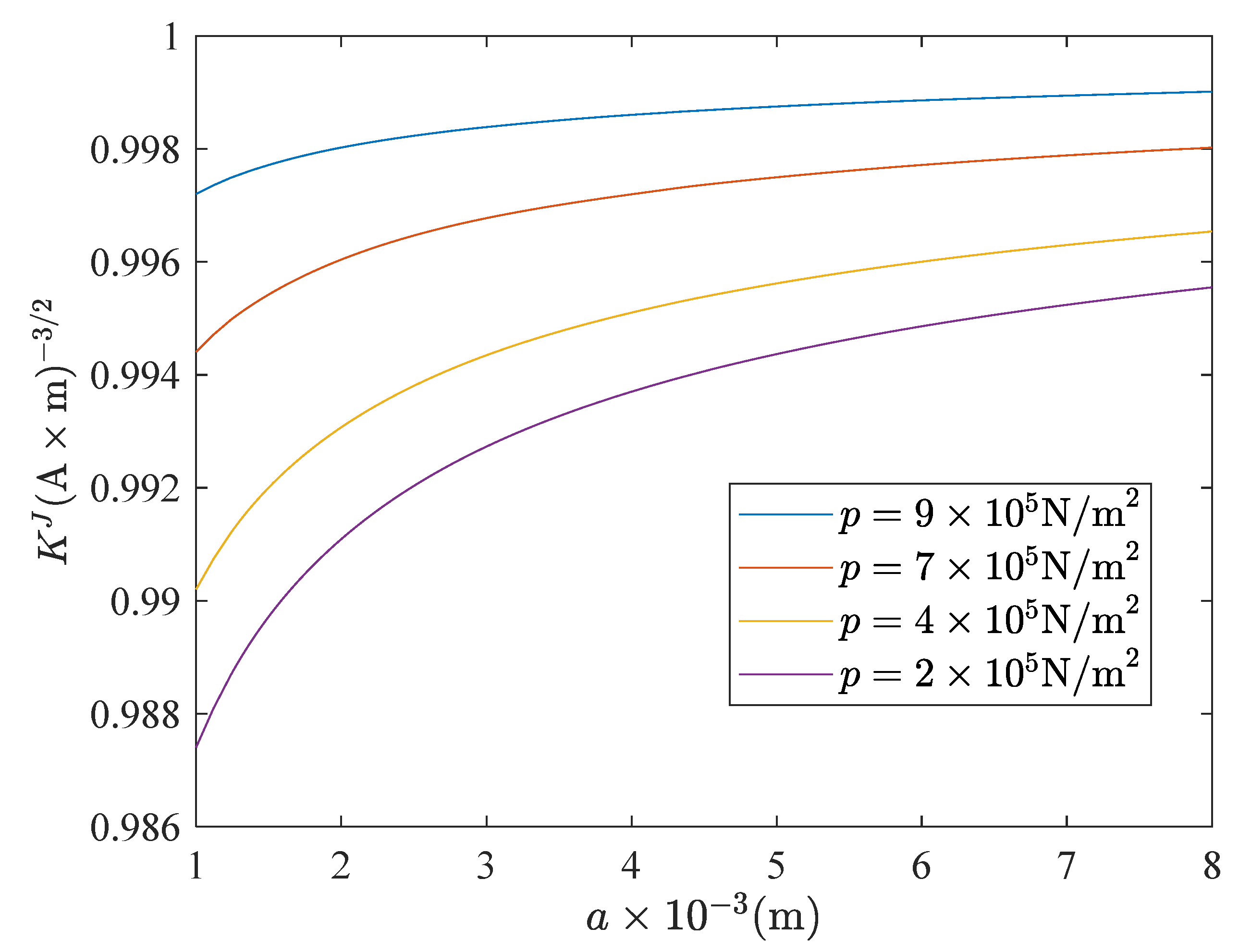
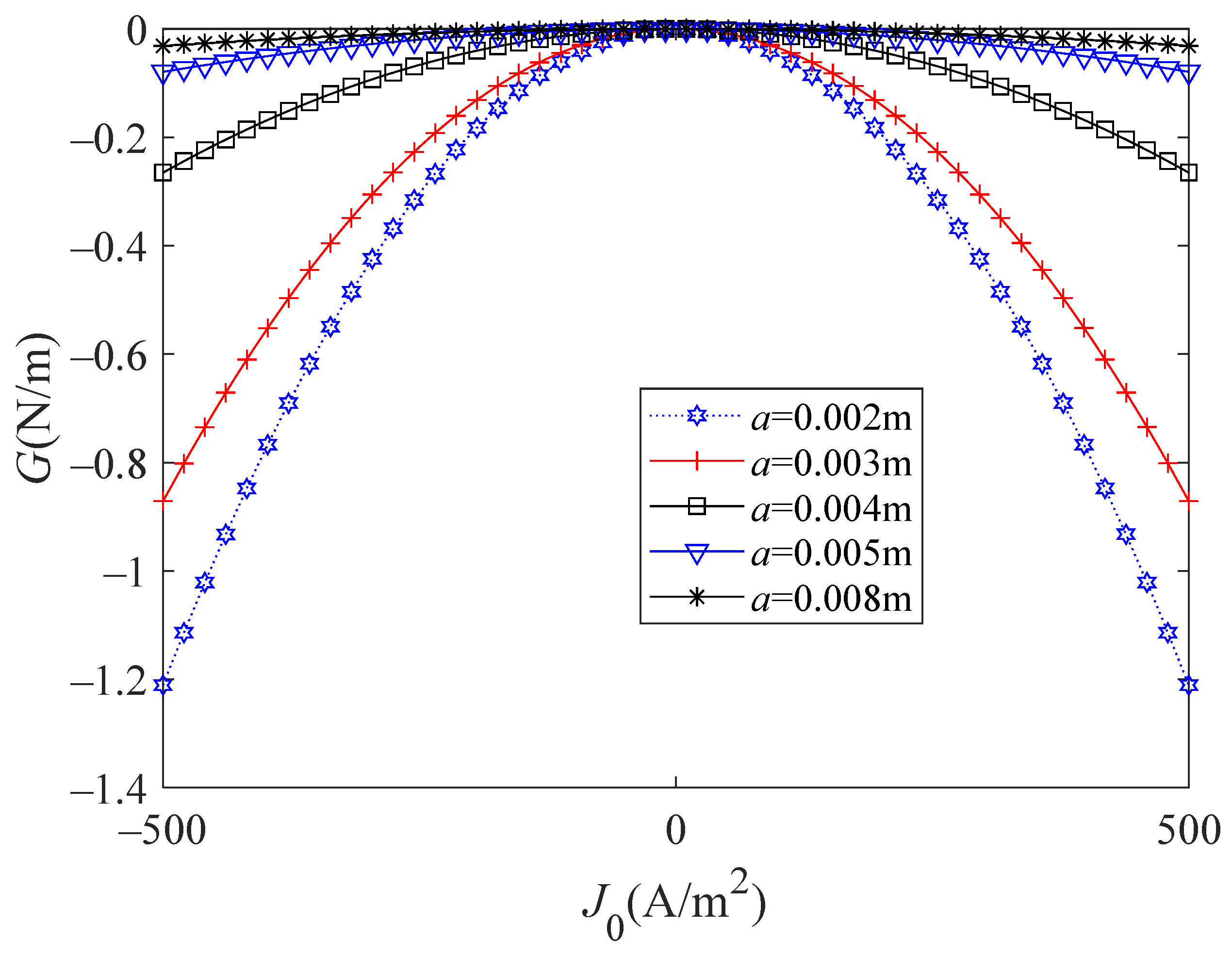
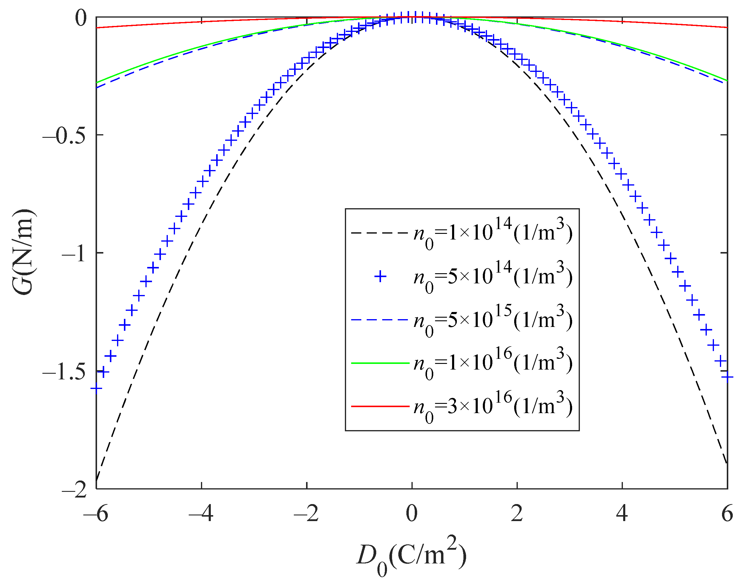
6. Numerical Analysis

ZnO, CdS and cadmium selenide are typical n-type PSCs due to their inherent defects. ZnO, with a thickness of h = 6 × 10⁻³ m and a crack length of 2a = 2 × 10⁻³ mm, is considered in this paper. The material parameters are [46,47]:
c 44 ( psc ) = 4.247 × 10 10   N / m 2 ,   e 15 = 0.48   N / m 2 ,   ε 11 = 7.570 × 10 11   F / m μ 11 = 0.02   m 2 / Vs ,   d 11 = 5.2 × 10 4   m 2 / s ,   c 44 ( e ) = 2.65 × 10 10   N / m 2 .
In Figure 2, variations in the stress intensity factor with 2a/h1 is depicted when n (x, y) = 0 and h1 = h2. It is evident that as 2a/h1 gradually increases, the stress intensity factor at the crack tip also increases, indicating a higher likelihood of crack propagation. These findings align with those reported in Ref. [23], thus reinforcing the consistency and validity of the results.
Figure 3 and Figure 4 depict the variations of the stress intensity factor and current density intensity factor at the crack tip with the crack length under different mechanical loads. As the crack length increases, both the stress intensity factor and current density intensity factor exhibit continuous growth. This trend indicates that longer cracks experience higher levels of stress and electrical current densities at their tips, indicating an increased likelihood of crack propagation. Furthermore, the influence of a mechanical load on these factors is evident. As the mechanical load increases, both the stress intensity factor and current density intensity factor also increase. This implies that higher mechanical loads exert a more significant effect on promoting crack propagation by intensifying stress and electrical activity at the crack tip. In summary, the observed trends underscore the critical role of crack length and mechanical load in determining the likelihood of crack propagation. The results suggest that longer cracks and higher mechanical loads contribute to increased stress and current density intensity factors, ultimately leading to a greater propensity for crack propagation.
Figure 5 depicts variations in the energy release rate at crack a end with the crack length under different current densities. The plot reveals that the energy release rate G can either increase or decrease, depending on the direction and magnitude of the current when the absolute value of the current density increases. Specifically, at J 0 = 0, the energy release rate of crack a end reaches a peak. However, as the electrical load increases further, there is a subsequent decrease in G. This indicates that a further increase in electrical load consistently suppresses crack growth, highlighting the complex interplay between current density and crack propagation dynamics.
Figure 6 shows variations in the energy release rate at crack a end and the current intensity under different carrier concentrations. It can be observed that G has a trend of increasing or decreasing, depending on the direction and magnitude of the electrical load. When the current density is zero, the energy release rate reaches the peak, and the crack is in the most dangerous situation. The results show that carrier concentration can accelerate or slow the crack propagation, depending on the current density. At a given carrier concentration, the presence of an electric load can also accelerate or slow the growth of the crack, depending on the direction, magnitude, and type of electric load.
Figure 7 illustrates variations in the energy release rate at crack a end with the electric displacement under different carrier concentrations. The plot reveals a consistent decreasing trend in the energy release rate G as the absolute value of the current density increases. This observation shows that higher current densities tend to suppress crack propagation.
Moreover, the results highlight the influence of carrier concentration on crack propagation dynamics, demonstrating that carrier concentration can either accelerate or decelerate crack propagation, depending on the magnitude of the electric displacement. The findings emphasize the significant impact of both current density and carrier concentration on the energy release rate and subsequent crack behavior, underscoring the intricate interplay between electrical properties and crack propagation in the material.

7. Conclusions

This paper establishes an anti-plane mechanical model of an interface crack between a strip of piezoelectric semiconductor and an elastic substrate. Two types of boundary conditions were considered, and the carrier density, current density, and potential shift near the crack were obtained through numerical calculations. By incorporating the coupling effect of external forces, electricity, and carriers, the expressions for displacement, electric potential, and carrier were derived using Fourier transform techniques. The results show that various factors, including thickness size, mechanical load, and electrical load, significantly influence the propagation of a crack. When the current density is zero, the energy release rate reaches its peak, and the crack is in its most dangerous state. As the absolute value of the current density increases, the energy release rate G continuously decreases. Moreover, the carrier concentration plays a crucial role in either accelerating or retarding crack propagation, depending on factors such as the direction, size, and the type of electric load applied. The research findings emphasize the complex interaction between mechanical and electrical properties in the context of crack propagation in piezoelectric semiconductor substrate structures. The obtained research results provide useful references for coating substrate structures.

Author Contributions

Methodology, X.T., Y.Z. and H.M.; Investigation, X.T., Y.Z. and S.D.; Writing—original draft, X.T.; Formal analysis, S.D.; Writing—review and editing, X.L.; Supervision, S.D.; Project administration, X.L.; Funding acquisition, X.L. All authors have read and agreed to the published version of the manuscript.

Funding

Project supported by the National Natural Science Foundation of China (Nos.12262033, 12272195), Ningxia Hui Autonomous Region Science and Technology Innovation Leading Talent Training Project of China (No.2020GKLRLX01), and the Natural Science Foundation of Ningxia of China (No. 2023AAC02003).

Data Availability Statement

No data was used for the research described in the article.

Conflicts of Interest

The authors declare no conflicts of interest.

References

  1. Yang, J. Analysis of Piezoelectric Semiconductor Structures; Springer International Publishing: Berlin/Heidelberg, Germany, 2020. [Google Scholar]
  2. Sun, L.; Zhang, Z.; Gao, C.; Zhang, C. Effect of flexoelectricity on piezotronic responses of a piezoelectric semiconductor bilayer. J. Appl. Phys. 2021, 129, 244102. [Google Scholar] [CrossRef]
  3. Tian, R.; Nie, G.; Liu, J.; Pan, E.; Wang, Y. On Rayleigh waves in a piezoelectric semiconductor thin film over an elastic half-space. Int. J. Mech. Sci. 2021, 204, 106565. [Google Scholar] [CrossRef]
  4. Guo, X.; Wei, P. Dispersion relations of in-plane elastic waves in nano-scale one dimensional piezoelectric semiconductor/piezoelectric dielectric phononic crystal with the consideration of interface effect. Appl. Math. Model. 2021, 96, 189–214. [Google Scholar] [CrossRef]
  5. Tian, R.; Nie, G.; Liu, J.; Pan, E.; Wang, Y. Love waves in a piezoelectric semiconductor thin film on an elastic dielectric half-space. Acta Mech. Solida Sin. 2023, 36, 45–54. [Google Scholar] [CrossRef]
  6. Han, C.; Lu, C.; Zhao, M.; Zhang, Q. Nonlinear finite element analysis of electromechanical behaviors in a piezoelectric semiconductor beam. Int. J. Non-Linear Mech. 2023, 149, 104311. [Google Scholar] [CrossRef]
  7. Fu, S.; Wu, H.; He, W.; Li, Q.; Shan, C.; Wang, J.; Du, Y.; Du, S.; Huang, Z.; Hu, C. Conversion of dielectric surface effect into volume effect for high output energy. Adv. Mater. 2023, 35, 2302954. [Google Scholar] [CrossRef]
  8. Zhang, G.; Yang, Z.; Li, X.; Deng, S.; Liu, Y.; Zhou, H.; Peng, M.; Fu, Z.; Chen, R.; Meng, D.; et al. Gamma-Ray Irradiation Induced Dielectric Loss of SiO2/Si Heterostructures in Through-Silicon Vias (TSVs) by Forming Border Traps. ACS Appl. Electron. Mater. 2024, 6, 1339–1346. [Google Scholar] [CrossRef]
  9. Yang, J. A semi-infinite anti-plane crack in a piezoelectric semiconductor. Int. J. Fract. 2004, 130, L169–L174. [Google Scholar] [CrossRef]
  10. Hu, Y.; Zeng, Y.; Yang, J. A mode III crack in a piezoelectric semiconductor of crystals with 6 mm symmetry. Int. J. Solids Struct. 2007, 44, 3928–3938. [Google Scholar] [CrossRef]
  11. Zhang, J.; Hu, Y. Analysis on the anti-plane deformations of a piezoelectric semiconductor plate with a hole. In Proceedings of the 2014 Symposium on Piezoelectricity, Acoustic Waves, and Device Applications, Beijing, China, 30 October–2 November 2014; IEEE: New York, NY, USA, 2014; pp. 106–109. [Google Scholar]
  12. Fan, C.; Yan, Y.; Xu, G.; Zhao, M. Piezoelectric-conductor iterative method for analysis of cracks in piezoelectric semiconductors via the finite element method. Eng. Fract. Mech. 2016, 165, 183–196. [Google Scholar] [CrossRef]
  13. Qin, G.; Lu, C.; Zhang, X.; Zhao, M. Electric current dependent fracture in GaN piezoelectric semiconductor ceramics. Materials 2018, 11, 2000. [Google Scholar] [CrossRef] [PubMed]
  14. Zhao, Y.; Zhou, C.; Zhao, M.; Pan, E.; Fan, C. Penny-shaped cracks in three-dimensional piezoelectric semiconductors via Green’s functions of extended displacement discontinuity. J. Intell. Mater. Syst. Struct. 2017, 28, 1775–1788. [Google Scholar] [CrossRef]
  15. Zhang, Q.; Fan, C.; Xu, G.; Zhao, M. Iterative boundary element method for crack analysis of two-dimensional piezoelectric semiconductor. Eng. Anal. Bound. Elem. 2017, 83, 87–95. [Google Scholar] [CrossRef]
  16. Zhao, M.; Li, X.; Lu, C.; Zhang, Q. Nonlinear analysis of a crack in 2D piezoelectric semiconductors with exact electric boundary conditions. J. Intell. Mater. Syst. Struct. 2021, 32, 632–639. [Google Scholar] [CrossRef]
  17. Zhao, X.; Zhou, L.; Liu, J. Transient responses of a mode-III crack in a piezoelectric semiconductor material. In Proceedings of the 2023 17th Symposium on Piezoelectricity, Acoustic Waves, and Device Applications (SPAWDA), Chengdu, China, 10–12 November 2023; IEEE: New York, NY, USA, 2023; pp. 1–5. [Google Scholar]
  18. Sladek, J.; Sladek, V.; Pan, E.; Young, D.L. Dynamic anti-plane crack analysis in functional graded piezoelectric semiconductor crystals. CMES-Comput. Model. Eng. Sci. 2014, 99, 273–296. [Google Scholar]
  19. Sladek, J.; Sladek, V.; Pan, E.; Wünsche, M. Fracture analysis in piezoelectric semiconductors under a thermal load. Eng. Fract. Mech. 2014, 126, 27–39. [Google Scholar] [CrossRef]
  20. Beom, H.G.; Jang, H.S. Interfacial wedge cracks in dissimilar anisotropic materials under antiplane shear. Int. J. Eng. 2012, 56, 49–62. [Google Scholar] [CrossRef]
  21. Ding, S.H.; Zhou, Y.T.; Li, X. Interface crack problem in layered orthotropic materials under thermo-mechanical loading. Int. J. Solids Struct. 2014, 51, 4221–4229. [Google Scholar] [CrossRef]
  22. Arshid, E.; Amir, S.; Loghman, A. On the vibrations of FG GNPs-RPN annular plates with piezoelectric/metallic coatings on Kerr elastic substrate considering size dependency and surface stress effects. Acta Mech. 2023, 234, 4035–4076. [Google Scholar] [CrossRef]
  23. Kwon, J.H.; Lee, K.Y. Crack problem at interface of piezoelectric strip bonded to elastic layer under anti-plane shear. KSME Int. J. 2001, 15, 61–65. [Google Scholar] [CrossRef]
  24. Ou, Z.C.; Chen, Y.H. Interface crack problem in elastic dielectric/piezoelectric bimaterials. Int. J. Fract. 2004, 130, 427–454. [Google Scholar] [CrossRef]
  25. Sladek, J.; Sladek, V.; Wünsche, M.; Zhang, C. Analysis of an interface crack between two dissimilar piezoelectric solids. Eng. Fract. Mech. 2012, 89, 114–127. [Google Scholar] [CrossRef]
  26. Pamnani, G.; Bhattacharya, S.; Sanyal, S. Analysis of interface crack in piezoelectric materials using extended finite element method. Mech. Adv. Mater. Struct. 2019, 26, 1447–1457. [Google Scholar] [CrossRef]
  27. Hu, S.; Li, J. Interaction between screw dislocation and interfacial crack in fine-grained piezoelectric coatings under steady-state thermal loading. Appl. Sci. 2021, 11, 11922. [Google Scholar] [CrossRef]
  28. Herrmann, K.P.; Loboda, V.V. Fracture mechanical assessment of interface cracks with contact zones in piezoelectric bimaterials under thermoelectromechanical loadings: I. Electrically permeable interface cracks. Int. J. Solids Struct. 2003, 40, 4191–4217. [Google Scholar] [CrossRef]
  29. Zhang, Z.; Zhang, B.; Li, X.; Ding, S. A closed-form solution to the mechanism of interface crack formation with one contact area in decagonal quasicrystal bi-materials. Crystals 2024, 14, 316. [Google Scholar] [CrossRef]
  30. Rizzoni, R.; Serpilli, M.; Raffa, M.L.; Lebon, F. A micromechanical model for damage evolution in thin piezoelectric films. Coatings 2023, 13, 82. [Google Scholar] [CrossRef]
  31. Golub, M.V.; Doroshenko, O.V. Analysis of eigenfrequencies of a circular interface delamination in elastic media based on the boundary integral equation method. Mathematics 2021, 10, 38. [Google Scholar] [CrossRef]
  32. Gu, B.; Yu, S.W.; Feng, X.Q. Transient response of an interface crack between dissimilar piezoelectric layers under mechanical impacts. Int. J. Solids Struct. 2002, 39, 1743–1756. [Google Scholar] [CrossRef]
  33. Kwon, J.H.; Lee, K.Y. Moving interfacial crack between piezoelectric ceramic and elastic layers. Eur. J. Mech. A/Solids 2000, 19, 979–987. [Google Scholar] [CrossRef]
  34. Gao, C.F.; Häusler, C.; Balke, H. Periodic permeable interface cracks in piezoelectric materials. Int. J. Solids Struct. 2004, 41, 323–335. [Google Scholar] [CrossRef]
  35. Feng, F.X.; Lee, K.Y.; Li, Y.D. Multiple cracks on the interface between a piezoelectric layer and an orthotropic substrate. Acta Mech. 2011, 221, 297–308. [Google Scholar] [CrossRef]
  36. Loboda, V.; Sheveleva, A.; Chapelle, F.; Lapusta, Y. Multiple electrically limited permeable cracks in the interface of piezoelectric materials. Mech. Adv. Mater. Struct. 2023, 54, 1–13. [Google Scholar]
  37. Zhu, S.; Yu, H.; Guo, L. Analysis of an interfacial crack between two nonhomogeneous piezoelectric materials using a new domain-independent interaction integral. Compos. Struct. 2024, 331, 117873. [Google Scholar] [CrossRef]
  38. Yu, H.; Zhu, S.; Ma, H.; Wang, J. Interface crack analysis of piezoelectric laminates considering initial strain. Int. J. Mech. Sci. 2024, 271, 109104. [Google Scholar] [CrossRef]
  39. Luo, Y.; Zhang, C.; Chen, W.; Yang, J. Piezotronic effect of a thin film with elastic and piezoelectric semiconductor layers under a static flexural loading. J. Appl. Mech. 2019, 86, 051003. [Google Scholar] [CrossRef]
  40. Ren, C.; Wang, K.F.; Wang, B.L. Electromechanical analysis of a piezoelectric semiconductor bilayer system with imperfect interface. Eur. J. Mech. -A/Solids 2024, 103, 105173. [Google Scholar] [CrossRef]
  41. Holzapfel, G.A. Nonlinear solid mechanics: A continuum approach for engineering science. Meccanica 2002, 37, 489–490. [Google Scholar] [CrossRef]
  42. Vasileska, D.; Goodnick, S.M.; Klimeck, G. Computational Electronics: Semiclassical and Quantum Device Modeling and Simulation; CRC Press: Boca Raton, FL, USA, 2017. [Google Scholar]
  43. Hutson, A.R.; White, D.L. Elastic wave propagation in piezoelectric semiconductors. J. Appl. Phys. 1962, 33, 40–47. [Google Scholar] [CrossRef]
  44. White, D.L. Amplification of ultrasonic waves in piezoelectric semiconductors. J. Appl. Phys. 1962, 33, 2547–2554. [Google Scholar] [CrossRef]
  45. Pak, Y.E. Crack extension force in a piezoelectric materia. J. Appl. Mech. 1990, 57, 647–653. [Google Scholar] [CrossRef]
  46. Auld, B.A. Acoustic Fields and Waves in Solids; John Wiley and Sons: Hoboken, NJ, USA, 1973; pp. 357–382. [Google Scholar]
  47. Goodge, M.E. Semiconductor Device Technology; The Macmillan Press: New York, NY, USA, 1983. [Google Scholar]
Figure 1. Schematic diagram of a coating substrate model with an interface crack.
Mathematics 12 01208 g001
Figure 2. Variations in stress intensity factor K σ with 2a/h1 (case 2) [23].
Mathematics 12 01208 g002
Figure 3. Variations in K σ with a for different p (case 1).
Mathematics 12 01208 g003
Figure 4. Variations in K J with a for different p (case 1).
Mathematics 12 01208 g004
Figure 5. Variations in G with J 0 for different a (case 1).
Mathematics 12 01208 g005
Figure 6. Variations in G with J 0 for different n 0 (case 1).
Mathematics 12 01208 g006
Figure 7. Variations in G with D0 for different n 0 (case 2).
Mathematics 12 01208 g007
Disclaimer/Publisher’s Note: The statements, opinions and data contained in all publications are solely those of the individual author(s) and contributor(s) and not of MDPI and/or the editor(s). MDPI and/or the editor(s) disclaim responsibility for any injury to people or property resulting from any ideas, methods, instructions or products referred to in the content.

