Abstract
Carbon monoxide (CO) gas is an odorless toxic combustion product that rapidly accumulates inside ordinary places, causing serious risks to human health. Hence, the quick detection of CO generation is of great interest. To meet this need, high-performance sensing units have been developed and are commercially available, with the vast majority making use of semiconductor transduction media. In this paper, we demonstrate for the first time a fabrication protocol for arrays of printed flexible CO sensors based on a printable semiconductor catalyst-decorated reduced graphene oxide sensor media. These sensors operate at room temperature with a fast response and are deposited using high-throughput printing and coating methods on thin flexible substrates. With the use of a modified solvothermal aerogel process, reduced graphene oxide (rGO) sheets were decorated with tin dioxide (SnO2) nanoscale deposits. X-ray diffraction data were used to show the composition of the material, and high-resolution X-ray photoelectron spectroscopy (XPS) characterization showed the bonding status of the sensing material. Moreover, a very uniform distribution of particles was observed in scanning (SEM) and transmission electron microscopy (TEM) images. For the fabrication of the sensors, silver (Ag) interdigitated electrodes were inkjet-printed from nanoparticle inks on plastic substrates with 100 µm linewidths and then coated with the SnO2-rGO nanocomposite by inkjet or slot-die coating, followed by a thermal treatment to further reduce the rGO. The detection of 50 ppm of CO in nitrogen was demonstrated for the devices with a slot-die coated active layer. A response of 15%, response time of 4.5 s, and recovery time of 12 s were recorded for these printed sensors, which is superior to other previously reported sensors operating at room temperature.
1. Introduction
Carbon monoxide (CO) is an acutely toxic gas as room temperature and ambient pressure that can accumulate in ordinary environments like homes and automobiles, causing poisoning and severe side effects in concentrations as low as 50 ppm. The detection of CO gas at low partial pressures is challenging, mainly due to the odorless and colorless nature of the gas, and high-performance sensors are usually required to guarantee a safe detection response. Currently, most commercial CO sensors are based on the semiconductor SnO2, since this technology affords a high response and robustness of operation [1]. Moreover, these semiconductor-based sensors possess the advantage of being produced through methods from the microelectronics industry, meaning they can be easily miniaturized. These characteristics have made SnO2-based CO sensors commercially attractive in some applications. However, the technology has some drawbacks. The manufacturing protocols for these sensors rely on expensive tools, subtractive processes, and highly controlled conditions (e.g., high temperature, etching, and multi-step processes). In addition, the bulk SnO2 sensor media typically must be heated to temperatures above 400 °C to achieve a sufficient CO response [2,3]. This temperature limit hinders the development of polymer film-supported flexible and thin devices.
In the last few years, two different approaches have been pursued to solve the problems mentioned above. These include the use of nano-sized SnO2 for easier processability and the use of supporting charge transport materials to decrease the sensor’s operating temperature. There have been a number of reports in literature of SnO2 nanoparticles dispersed in fluids and SnO2-based thin film devices produced by solution processing, very often with improved responses [4,5]. A very attractive possibility implied by these materials and thin film structures, which is explored in the present work, is the use of printing techniques for the fabrication of devices [6]. For instance, screen [7,8,9] and inkjet [10,11,12] printing have been used to quickly prototype SnO2-based sensors. Although the solution-processing of SnO2 was demonstrated, in all of the prior work either a high-temperature processing step is necessary for activating the SnO2 nanopowder or a heater is employed to increase the response at the point of use.
To improve the conductivity and afford lower operating temperatures, charge transport materials have been combined with SnO2 in gas sensor media [5]. In this regard, graphene has been used extensively. In one instance, Mao et al. have used SnO2 to modify reduced graphene oxide (rGO) and tune the response of resistance- and transistor-based sensors to ammonia and NO2, obtaining a high response (~5 ppm) and short recovery time (~30 s) [13]. Using a similar approach, the same group subsequently reported transistor-based CO sensors consisting of single-walled carbon nanotubes (SWCNT) decorated with SnO2 nanoparticles [14]. In this case, the CO detection limit was 1 ppm and the recovery time for a CO concentration of 100 ppm was only 2 s. Liu et al. [15] employed a graphene aerogel method [16,17] to synthesize a purely resistive NO2 sensor with similar properties to the one reported by Mao et al. [13]. Interestingly, the sensing units reported by Liu et al. showed a high response towards NO2 concentrations as low as 10 ppm but showed a negligible response to other gases, including CO [15]. Although low-temperature sensing and solution-processed devices are reported in these and other publications, the fabrication protocols employed for partial or sometimes full sensor fabrication are neither scalable nor of high technological viability.
In the present manuscript, we report the formulation of a nanoink composed of a high response SnO2-decorated rGO that can be deposited using high-throughput printing and coating methods. With the use of high-resolution inkjet-printed Ag electrodes on plastic substrates, we demonstrate for the first time a fully printed, flexible sensor that is capable of detecting relevant concentrations of CO at room temperature and is fabricated though scalable methods.
2. Materials and Methods
2.1. Synthesis of SnO2-Decorated Reduced Graphene Oxide (SnO2-rGO) Aerogel and Ink Formulation
A solvothermal process adapted from [15] was used to synthesize the nanomaterial for the active layer of the sensors fabricated in this work. This process leads to the formation of nanoscale SnO2 deposits on the surface of porous, conductive graphene aerogels [16,17]. As will be discussed later, the same procedure allows for the concomitant reduction of graphene oxide and results in the higher conductivity of the films.
In a typical synthesis, 20 mg of graphene oxide (CheapTubes, Inc., Grafton, VT, USA) is initially suspended in 20 mL of ethylene glycol (Sigma-Aldrich, St. Louis, MO, USA, analytical grade) and the suspension is sonicated for 30 min to improve the dispersion and exfoliate the material. Subsequently, 5 nmol of tin chloride pentahydrate (SnCl2·H2O, Sigma-Aldrich, analytical grade), 0.99 g of sodium acetate (Sigma-Aldrich, analytical grade), and 0.11 g of sodium citrate (Sigma-Aldrich, analytical grade) are added to the suspension, which is vigorously stirred for 120 min at 60–70 °C. Finally, the suspension is transferred to a 50 mL Teflon-lined autoclave and heated at 200 °C for 10 h. The SnO2-graphene oxide (SnO2-rGO) nanocomposite hydrogel product is a black solid that precipitates from the suspension. The hydrogel is collected by centrifugation and purified by freeze-drying for 10 h. All the reagents used in this work were analytical grade and were used as purchased without any further purification.
The product of the syntheses was characterized by X-ray diffractometry (XRD) using a Bruker D8 Discover instrument with a Cu Kα source. The morphology of the final material was imaged using both transmission and scanning electron microscopy (TEM and SEM), respectively, in a Tecnai G2 F20 instrument from FEI and a XL830 Dual-Beam SEM/FIB (5–10 kV) instrument from Altura. The samples for TEM were obtained by drop-casting a suspension of the material in acetone onto a lacey carbon net with a copper mesh backing. For the SEM analysis, the powder was sprayed onto a double-adhesive carbon tape and the latter was glued to the sample holder. Energy-dispersive X-ray (EDX) spectroscopy data were collected in parallel with the SEM imaging using an Oxford X-max detector. An X-ray photoelectron spectroscopy (XPS) characterization was also conducted for a detailed study of the atomic bonding and degree of reduction of the graphene oxide sheets. Measurements were carried out in equipment from Surface Science Instruments (S-Probe) using a monochromatic Al Kα X-ray source, which was operated at 20 mA and 10 kV, and a low energy electron flood gun for charge neutralization. Service Physics Hawk version 7 data analysis software was used for data fitting and calculating the elemental compositions from peak areas. Drop-cast films of SnO2-rGO in n-methyl pyrrolidone (NMP) subjected to different post-processing treatments (detailed in Section 2.2.2) were employed.
The inks used to fabricate the devices studied here were produced by the re-dispersion of the purified SnO2-rGO aerogel. To improve the dispersion quality and stability, the aerogel was firstly ground using a mortar and pestle and then different solvents were tested, including NMP, ethylene glycol, and ethanol. In several cases, sonication was performed for 10–12 h to obtain a good and stable dispersion. The final ink had its surface tension and viscosity characterized using, respectively, a DSA100 tensiometer from Kruss and a DV3T rheometer from Brookfield.
2.2. Device Fabrication
2.2.1. Inkjet-Printed Ag Electrodes
A co-planar interdigitated electrode structure (IDEs) was selected for the resistance-based sensors fabricated in this work because of the high active-area per unit electrode-area, compatibility with thin flexible substrates, and miniaturized dimensions achievable in this device layout. The IDEs were printed on plastic substrates, including poly(ethylene theraphthalate) (PET–FOM Technologies, Copenhagen, Demark) and poly(imide) (Kapton XF-101, Polyonics, Westmoreland, NH, USA), using a Dimatix DMP-2800 inkjet printer from Fujifilm and a commercial nanoparticle-based silver (Ag) ink from Advanced Nano Products (Pleasanton, CA, USA) (Silverjet DGP-40TE-20C). The substrates were cleaned with isopropyl alcohol immediately before printing. The center-to-center spacing between the immediately adjacent printed drops was 40 microns. After ambient atmosphere drying on the printing bed, the electrodes were sintered at 120 °C for 10 min in a convection oven. A four-terminal structure was used to eliminate contributions from contact resistance to the sensing measurements.
2.2.2. SnO2-rGO Active Layer Printing and Coating
Inkjet-printing and slot-die coating were used to deposit sensor active layers from the SnO2-rGO ink. The printing process and coating process were conducted on the top of the as-printed silver electrodes. The inkjet experiments were conducted with a Dimatix DMP-2800 printer, using 16V for the nozzle actuation, a table temperature of 44 °C, and a drop spacing of 40 µm. Multilayer overprinting was used to reduce the sheet resistance of the printed features. The inkjet ink was a 2 mg/mL dispersion of SnO2-rGO in n-methyl pyrrolidone (NMP) that was sonicated for 9 h to produce a fully exfoliated rGO [16,18]. Substrates containing previously printed electrodes were treated by UV-Ozone for 5 min. Slot-die coating experiments were performed using a mini-roll coater (MRC) from FOM Technologies with a 13-mm wide meniscus guide plate for the slot. In this case, a 2.5 mg/mL dispersion of SnO2-rGO in ethylene glycol was employed. The viscosity of the dispersion was 16.43 cP at 25 °C. The drum temperature of 120 °C and speed of 41.67 cm/min were employed in the experiments, and the solution pumping rate was 40 µL/min. Thicker, non-printed films were deposited by drop-casting as a control.
Post-printing treatments to improve the graphene oxide reduction and increase the film conductivity were conducted using two different convection oven protocols: (i) annealing at 200 °C for 30 min and (ii) annealing at 120 °C for 12 h.
2.3. CO Sensing Measurements
Carbon monoxide (CO) sensing was performed in a sealed chamber that was initially evacuated and then refilled, with a constant and continuous flow of 5.5 L/min provided by a regulator coupled to a flowmeter. The test chamber was placed in an environmentally controlled room, which had a temperature maintained at 24.2 °C (±0.2 °C) and a relative humidity at 20%. The target test gas was 50 ppm CO balanced with nitrogen. The selectivity test was conducted under 5% hydrogen balanced with nitrogen. To eliminate the side effect of nitrogen, the devices were then tested with 99.995% nitrogen. The gases above were all purchased from Praxair, Inc. Pure carbon dioxide (CO2) test gas was obtained from the reaction of dilute hydrochloric acid and baking soda. Between each test, the chamber was purged with synthetic dry air. Resistivity measurements were recorded using a probe-station with four microtips and a Keithley 2400 source meter. A 4-point ohmmeter setup was applied to get an accurate resistance reading from the devices. A current of 1 μA was applied to the two force terminals of the sensor, and the voltage drop across two opposite sensing terminals was measured by the tool within a compliance limit of 21 V. The measurements were carried out in duplicate for each of the sensors tested.
3. Results
3.1. SnO2-rGO Composition and Manostructure
As mentioned, the solvothermal process to synthesize SnO2-rGO composites was previously reported in the literature [15]. When attempts were made to replicate this process in this work, however, only a modest loading of SnO2 on the rGO was achievable. Films made from this material had a high resistance (~1 MΩ) and ca. 25% less response when compared with other strategies reported below. In a first attempt to improve the material homogeneity and particle loading, the proportion of reagents used for the SnO2 synthesis (SnCl2, sodium acetate, and sodium citrate) relative to the graphene oxide was doubled. This caused the formation of SnO2 nanoparticles that were not attached to the rGO sheets, which was attributed to the rapid homogenous nucleation of SnO2 at the beginning of the reaction. To avoid this situation, a two-step synthesis was employed that included the vigorous stirring of the reagents in solution at 60 to 70 °C prior to the higher temperature second reaction stage. This approach yielded better results in terms of SnO2 loading, dispersion, and nucleation onto graphene sheets, as determined by TEM. After coating with inks made with the reaction product, the deposited films were annealed to further reduce the graphene oxide. The efficiency of this annealing is indicated by the XPS data in Table 1. The high reduction rate of the graphene oxides contributed to achieving the room-temperature working/measuring environment. Additionally, the conductivity of the sensing materials was increased for films that were annealed, and much thinner films could be used without reaching the limit of electric resistance of our measuring system (~106 Ω), which hence resulted in an improved gas response.

Table 1.
C:O atomic ratio calculated from the XPS spectra obtained for the drop-cast films from NMP dispersions. All the samples were dried in an oven at 70 °C for 30 min and some of them were then submitted to the extra post-treatment step, as indicated. GO = commercial graphene oxide; r-GO = reduced graphene oxide, submitted to the solvothermal process for reduction; SnO2/r-GO = SnO2 decorated reduced graphene oxide. * C:O ratio for SnO2-containing samples was calculated by subtracting the oxygen atoms linked to Sn.
XRD was used to characterize the structural composition of the SnO2-rGO nanocomposite material. In Figure 1, four major SnO2 peaks can be seen in the XRD diffraction spectra centered at 2θ values around 27° (110), 33° (101), 52° (211), and 65° (112), indicating the successful of syntheses of the rutile-structured SnO2 [19,20]. As expected, there was no visible diffraction peak from graphite at 10.4°, indicating an effective GO reduction and concomitant graphene sheet dispersion [20,21]. Moreover, the dispersion was enhanced by the deposition of nano-scaled SnO2 crystals. It effectively suppressed the restacking of graphene layers. The latter is highly desirable when using graphene oxide-based materials in sensors because of the improved response afforded by the higher surface area/volume ratios [15]. Such improved porosity is confirmed by the optical characterization that follows.
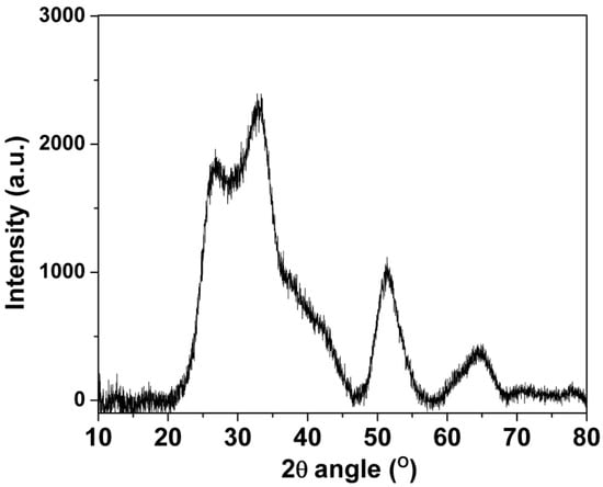
Figure 1.
X-ray diffraction data for the SnO2-rGO composite synthesized in this work.
The SEM picture in Figure 2A indicates that the microstructure of the resulting SnO2-rGO is composed of an interconnected 3D network. Similar microstructures were observed previously for modified SnO2-rGO derived from a freeze-drying process [15]. Interestingly, we note from Figure 2A that the material can preserve this microstructure even after being milled and re-dispersed in NMP during the ink preparation protocol used in this work. In the SEM picture in Figure 2B and the TEM pictures in Figure 2C,D higher magnification images of the same sample are shown. In these images, semi-spherical SnO2 nanoparticles can be seen decorating the surface of the rGO sheets. Such nanoscale deposits appear as white spots in the SEM image and as black dots in the TEM pictures. Their distribution on the surface of the reduced GO is more uniform in Figure 2D, where a two-step synthesis procedure was used, than in Figure 2C, where a one-step synthesis was conducted. The compositional uniformity was confirmed by EDX measurements taken in parallel with the SEM characterization (Figure 3). The spectrum in Figure 3A, obtained from the area indicated in Figure 3B, shows that C, O, and Sn are the major constituents of the material, as expected. Moreover, when Sn and C are marked, respectively, in red and green in a SEM-EDX map (Figure 3B), it is clearly seen that the SnO2 deposits are, in fact, well dispersed over the surface of the rGO sheets. Such improved loading and dispersion of the nanoscale deposited were obtained only with the two-step synthesis protocol.
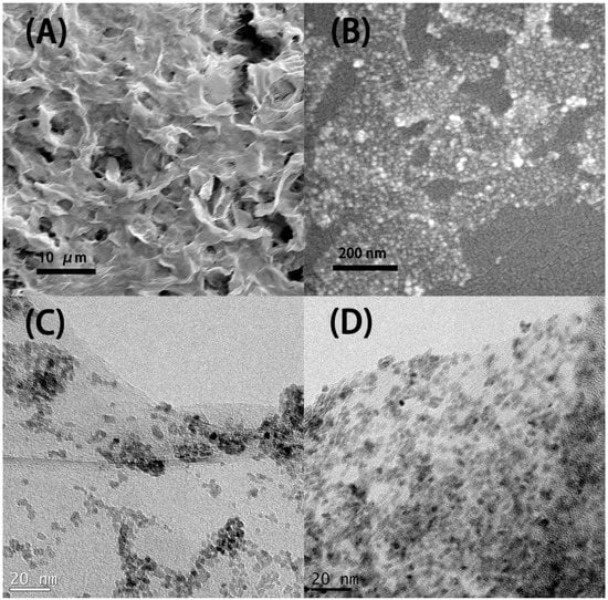
Figure 2.
SEM (A,B) are images of the SnO2-decorated rGO synthesized by the modified two-step process. TEM (C) is the image of the SnO2-decorated rGO synthesized by the traditional one-step process. (D) is the image of the SnO2-decorated rGO synthesized by the modified two-step process. The modification in the two-step process resulted in a more uniform distribution and higher loading rate of the SnO2 nanoparticles. Samples were prepared from dispersions of the material in n-methyl pyrrolidone (NMP).
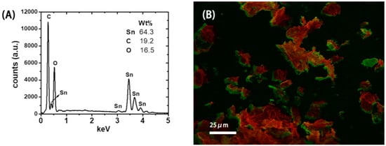
Figure 3.
(A) Energy-dispersive X-ray (EDX) spectrum showing the main atomic composition of the SnO2-reduced graphene oxide (rGO) material. (B) SEM-EDX map showing the distribution of Sn (red) and C (green).
High-resolution X-ray photoelectron spectroscopy (XPS) spectra were collected to determine the nature of the chemical bonding in the SnO2-rGO nanocomposite material. Regions of the spectra for elements of interest were fitted and deconvolved. Figure 4A shows that the C1s peak between 283 eV and 292 eV possesses contributions from three separate peaks, indicating the presence of C atoms involved in carboxyl, ether-like C-S, and C-C bindings, respectively. The O1s peak between 529 and 536 eV in Figure 4B in turn indicates the presence of carbonate and hydroxide groups and metal oxide bonds. Finally, the Sn3d region of the spectrum in Figure 4C displays two peaks centered at 487–488 eV and 496 eV, which are attributed to Sn 3d electrons with 5/2 and 3/2 spins, respectively, and are typical for SnO2-graphene composites [22].
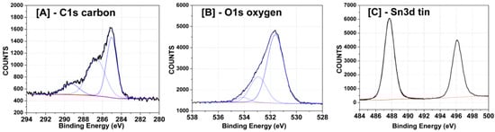
Figure 4.
High-resolution XPS scans for the selected SnO2-graphene peaks assigned to (A) carbon; (B) oxygen; (C) tin. Peaks were fitted and deconvoluted using Hawk analysis software.
All the XPS peaks and assignments in Figure 4 were previously described in literature [23] and afford a clear idea of the atomic bonding in the material. The oxygen peaks in Figure 4B indicate both that SnO2 has its chemical structure preserved, since metal oxide bonds are seen, and that graphene oxide is in fact not completely reduced in the conditions used, since carboxyl, hydroxyl, and ether groups are present [23]. Moreover, from the absence of Sn-C around 192 eV in Figure 4C, we conclude that SnO2 is linked to rGO mainly through bonds between Sn and O atoms in the graphene structure and possibly through some oxygen (from SnO2) to carbon bonds. The latter is advantageous for sensing, since Sn does not form direct bonds with C and is available to interact with CO. The presence of C-S links in Figure 4A (the second peak in the spectrum) suggests the existence of some residual sulfuric acid (H2SO4), probably originating from the autoclave used during the synthesis (H2SO4 was used to wash the liners in the oven between experiments) or from synthesizing GO using Hummer’s method [24]. The content of the sulfur elements presenting in the SnO2/rGO samples is only 0.606%. All other chemical links between the different atoms in the structure are as expected.
XPS was also used to characterize the extent of graphene oxide reduction under different conditions. The carbon-to-oxygen (C:O) atomic ratios extracted from spectra from different samples (submitted to different treatments) are shown in Table 1. From the comparison of GO (graphene oxide—line 1) with the samples SnO2/r-GO one-step (line 3) and SnO2/r-GO two-step (line 4), we can clearly see that GO reduction is concomitantly happening during the solvothermal process along with SnO2 nanoparticle synthesis, since the C:O ratio for graphene oxide was increased from 2.4 to 5.0 (SnO2/r-GO one-step) or 12.1 (SnO2/r-GO two-step). Such an effect from reaction conditions is confirmed by a control sample (r-GO—line 2) in which GO was subjected to the same protocol used for the one-step synthesis of SnO2/r-GO, but without SnCl2 added to the medium. In this case, the C:O proportion rose to a similar level (5.5) as for the SnO2/r-GO one-step.
The beneficial effect of the two-step solvothermal synthesis of SnO2-rGO is also confirmed by the data in Table 1. The SnO2/r-GO two-step (line 4) presents a significantly higher C:O ratio than SnO2/r-GO one-step (line 3), indicating that the additional stirring step not only improved the distribution of SnO2 (see discussions for Figure 2 and Figure 3), but also facilitated the reduction of graphene. The SnO2/rGO one-step samples results correspond to Figure 2C and the SnO2/rGO two-step sample results correspond to Figure 2D. Additional post-treatment methods performed at 120 °C for 12 h or at 200 °C for 30 min were also used to improve the chemical reduction of GO. We can clearly see that 200 °C for 30 min allowed for a higher extent of graphene reduction, with the C:O ratio increasing to 16.6. Although such treatment is incompatible with one of the substrates tested here (PET–with an effective maximum process temperature of approximately 150 °C), it is suitable for sensor fabrication on polyimide (Kapton) films, and the shorter processing time is attractive for the overall fabrication protocol.
3.2. Inkjet-Printed Electrodes and Active Layer
The printing and coating techniques were used in this work to fabricate an electronic sensor for CO mainly due to their high-throughput and the possibility of making a device through a large-area scalable process [6]. Interdigitated electrode structures (IDE) were used, since they afford an increased active area for relatively small resistance-based devices. In this case, inkjet is an appropriate printing method for allowing the high-resolution printing of flexible metal traces using commercially available nanoparticle-based inks [25]. Arrays of high-resolution, flexible Ag IDEs were printed on PET and Kapton, with an example shown in Figure 5A. The line-width and spacing for the digits were both around 100 µm, the thickness was between 300 and 400 nm, and the resistivity after sintering was 3.52 × 10⁻⁵ Ω·cm (22.1% of pure Ag).
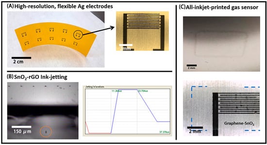
Figure 5.
(A) Inkjet-printed Ag Interdigitated electrode structures (IDEs) arrays on Kapton; (B) successful jetting of a single droplet of the SnO2-rGO dispersion in NMP (left) and the respective waveform used for that (right); (C) 1-layer inkjet-printed film of SnO2-rGO on bare poly(ethylene theraphthalate) (PET) (top) and 2-layers inkjet film of SnO2-rGO on Ag IDEs (bottom). Blue traced lines are included to guide the eyes on the last picture, due to the low contrast in the optical microscopy image.
Inkjet printing was also explored for depositing the active layer of the devices. The SnO2-rGO material was re-dispersed in NMP, producing a dark-blue dispersion with a viscosity of 1.93 cP and a surface tension of 38.6 mN/m that was stable for days. Although we were not able to filter this dispersion through 0.45 µm syringe filters, the same could be effectively jetted using 10 pL cartridges in the Dimatix printer at a frequency of 10 kHz, using a firing voltage of 16 V and the waveform shown in Figure 5B. Additionally, shown in Figure 5B is a stroboscopic optical image of a droplet ejected from one of the nozzles. The reproducible droplet distance from the nozzle in the stroboscopic imaging and the absence of “tailing” or satellite droplets indicates stable jetting at the target speed of 5–7 m/s, which is necessary for high fidelity electrode patterning.
A number of other parameters also had to be optimized for inkjet-printing a continuous layer of SnO2-rGO on PET and Kapton. Initially, severe dewetting was observed during the printing of NMP dispersions, and this was mostly mitigated by the introduction of a surface treatment step with UV-Ozone for 5 min. A picture of a single layer of SnO2-rGO printed on PET is shown in Figure 5C—top. Similar films with one or two layers of SnO2-rGO were also deposited on top of the active area of the IDEs previously printed (Figure 5C—bottom). The thicknesses of such films, probably under 100 nm per layer, could not be reproducibly measured with a stylus-based profilometer. Thicker films with up to 10 layers were also deposited, but their homogeneity was dramatically reduced in comparison with the thinner ones. For the reason mentioned above, inkjet-printing is considered sub-optimal for the deposition of the active layer, and further optimizations would be necessary for that. Therefore, slot-die coating was explored to fabricate the SnO2-rGO active layer.
3.3. Slot-Die Coated SnO2-rGO Film
Slot-die coating was also used to deposit the SnO2-rGO active layers for the flexible CO sensors studied here. Although this technique does not allow for digital patterning, it is higher throughput than inkjet and it was considered adequate to deposit the active layer of the sensors, since no complex patterning was required. In this case, the SnO2-rGO was dispersed in ethylene glycol and coated in a single < 20 s pass over 10 sets of IDEs inkjet-printed in a line on the substrate. In Figure 6, the roll-based setup for slot-die coating is shown on the left; a photo of the final sensor is shown at the center; and an array of the final sensors, fully printed in less than 2 h, is shown on the right. The thickness of the slot-die coated active layer is around 200–300 nm. The testing of these sensors, and of the all-inkjet-printed devices described in Section 3.4, for the detection of CO is described in the next section.
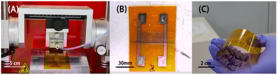
Figure 6.
(A) slot-die coating setup, showing the coating head during the deposition process on top of IDEs pre-printed on Kapton; (B) a single IDE with the active area (digits) coated by the SnO2 -rGO composite; (C) final array of ca. 30 flexible sensors for CO.
3.4. CO Sensing
The flexible gas sensors fabricated here were tested against a concentration of 50 ppm of CO (balanced with N2). The amount of 50 ppm CO is a threshold limit for the intoxication of humans [26]. The response (S) values reported are defined as the decrease in resistance (initial film resistance, R0, minus film resistance under CO exposure, Rf) divided by the original resistance, R0 (). Moreover, to facilitate comparisons, the sensing curves (shown in Figure 7) were further normalized to R0. Other important characteristics of the sensors are their response and recovery times, measured by the speed with which resistance readings transition between equilibrium values (within 10% of those), measured with or without exposure to CO.
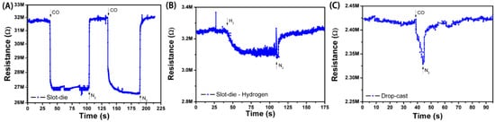
Figure 7.
Detection curves for: (A) slot-die coated film of SnO2-rGO against CO; (B) slot-die coated film of SnO2-rGO against H2; (C) drop-cast film of SnO2-rGO against CO.
The individual sensors with inkjet-printed active layers showed a relatively unstable response to CO. The inkjet-printed sensors were highly resistive when just a few layers (one or two) of SnO2-rGO were deposited for the active layer, and this high resistance was maintained even after thermal post-treatment. With an increased number of overprinted SnO2-rGO layers (ca. 10) in conjunction with sintering at 120 °C for 12 h, the resistance was lowered to ~10.2 MΩ. The film morphology, however, was inhomogeneous and the detection curves very irreproducible, with a noted response to temperature and humidity. New formulations based on different solvents and including additives are currently being explored in order to fabricate higher-performance, all-inkjet-printed sensors. Below, sensors with active layers fabricated by slot-die coating are discussed.
Figure 7A shows a sensing curve for an all-printed device in which the active layer was deposited by slot-die coating. A significant change in the resistance of the film was observed with exposure to CO, and this change could be repeatedly reversed by a subsequent exposure to N2. The normalized response in this case was ~15%, which is higher than for similar non-printed CO sensors reported in the literature [4], and the response and recovery times of 4.5 s and 12 s were observed. The response was reduced (ca. 12%) for slot-die-coated devices in which SnO2-rGO material synthesized in a one-step process was used (results not shown). This result indicates that our additional synthesis step, known to promote the better loading, dispersion, and nucleation of SnO2 nanodeposits onto graphene sheets (see Section 3.1), also results in improved sensing properties. The sensing performance of the drop-cast devices, SnO2/r-GO one-step slot-die-coated devices, and SnO2/r-GO two-step slot-die-coated devices are presented in Table 2.
Table 2.
Sensing performances of the drop-cast devices, SnO2/r-GO one-step slot-die-coated devices, and SnO2/r-GO two-step slot-die-coated devices.
The specificity of the all-printed sensor to CO was demonstrated primarily through a control measurement in which the device was tested in presence of H2 (Figure 7B). Upon H2 exposure, a much smaller variation of resistance (ca. 4%) was recorded, demonstrating the higher reactivity of CO molecules towards SnO2. A test for CO with a sensor having only rGO in the active layer (no SnO2) showed sensitivities of only 2−4% (results not shown). The specificity was further attested to by additional sensor tests against pure N2, CO2, and air, where <1% variations in film resistance were observed. Altogether, these results are consistent with a sensing mechanism where CO molecules are first adsorbed on the surface of the SnO2-rGO material and then oxidized to CO2 through a reaction that consumes electrons and oxygen [3]. This leads to an increase in the carrier concentration in graphene and a measurable change in resistance. Such a reaction is facilitated and can happen at room temperature due to the high surface area of junctions formed between the graphene molecules and SnO2 [13,15].
In one last control measurement, the sensing response for CO was also measured for a sensor in which the active layer was deposited by drop-casting instead of slot-die coating (Figure 7C). The response, response time, and recovery time for this device are, respectively, 7%, 6 s, and 14 s. This significantly lower performance is attributed to differences in thickness between the coated and cast devices. The cast device is six times thicker than the coated device, resulting in a reduced volume-to-surface area ratio and longer diffusion distances for CO to permeate the film. The fact that thinner film active layers result in a higher sensing response is also reported in literature [27].
4. Discussion
An innovative SnO2-decorated graphene oxide nanocomposite with improved SnO2 nanodeposits loading and distribution has been synthesized here through a modified solvothermal method, including a high-temperature step with vigorous stirring. This nanocomposite material has been formulated into inks and deposited on IDE sensor structures using digital (inkjet) and large-area (slot-die) printed films. A scalable, high-throughput, roll-to-roll (R2R)-compatible fabrication protocol for arrays of flexible sensors has been demonstrated. Sensors produced using these processes were tested for their detection of CO and showed a good response, rapid response time, and good reversibility. Control measurements confirmed the selectivity imparted by SnO2 and the improved performance of thinner, printed SnO2-rGO films. The sensors reported here operate at room-temperature, are thin and flexible, and can be additively fabricated through scalable, cost-effective protocols that can enable innovative applications and their integration into different products.
Author Contributions
J.Z. conceived the concept of this paper, carried out the experiment, and analyzed the data. S.T. carried out the experiment regarding the electrode inkjet printing. D.M. and T.M. encouraged J.Z. to investigate the reduction process and printing process of reduce graphene oxides. M.L. helped developing the hydrothermal reaction to synthesize the SnO2-rGO. B.R. provided support to the device printing process. F.P. conceived the idea, and provided support in inkjet printing process. D.M. and P.P. helped conceiving the idea, designing the experiment and optimizing the synthesis and fabrication process. All authors discussed the results and contributed to the final manuscript. All authors have read and agreed to the published version of the manuscript.
Funding
This research was funded with resources from the Washington Research Foundation (WRF) through a start-up budget provided to J. Devin MacKenzie. The authors are also grateful to the support from the Clean Energy Institute (CEI) of the University of Washington (UW) and the Washington Clean Energy Testbeds (WCET), where most of the work was conducted.
Conflicts of Interest
The authors certify that they have no affiliations with or involvement in any organization or entity with any financial interest or non-financial interest in the subject matter or materials discussed in this manuscript.
References
- Hawley, C. Toxic Gas Sensors. In Hazardous Materials Air Monitoring and Detection Devices, 2nd ed.; Hawley, C., Ed.; Delmar, Clifton Park, Jones and Bartlett Learning: Burlington, MA, USA, 2007; p. 43. [Google Scholar]
- Smith, R.L.; Hobbs, B.S.; Watson, J. Sensors, Nanoscience, and Instruments. In Sensors, Nonsocial. Biomed. Eng. Instruments; Dorf, R.C., Ed.; CRC Press: Boca Raton, FL, USA, 2006. [Google Scholar] [CrossRef]
- Harrison, P.G.; Willett, M.J. The mechanism of operation of tin(iv) oxide carbon monoxide sensors. Nature 1988, 332, 337–339. [Google Scholar] [CrossRef]
- Li, C.; Lv, M.; Zuo, J.; Huang, X. SnO2 Highly Sensitive CO Gas Sensor Based on Quasi-Molecular-Imprinting Mechanism Design. Sensors 2015, 15, 3789–3800. [Google Scholar] [CrossRef] [PubMed]
- Srivastava, V.; Jain, K. At room temperature graphene/SnO2 is better than MWCNT/SnO2 as NO2 gas sensor. Mater. Lett. 2016, 169, 28–32. [Google Scholar] [CrossRef]
- Pavinatto, F.J.; Paschoal, C.W.; Arias, A.C. Printed and flexible biosensor for antioxidants using interdigitated ink-jetted electrodes and gravure-deposited active layer. Biosens. Bioelectron. 2015, 67, 553–559. [Google Scholar] [CrossRef] [PubMed]
- Bakrania, S.D.; Wooldridge, M.S. The Effects of Two Thick Film Deposition Methods on Tin Dioxide Gas Sensor Performance. Sensors 2009, 9, 6853–6868. [Google Scholar] [CrossRef]
- Martinelli, G.; Carotta, M. Influence of additives on the sensing properties of screen-printed SnO2 gas sensors. Sens. Actuators B Chem. 1993, 16, 363–366. [Google Scholar] [CrossRef]
- Bârsan, N.; Weimar, U. Understanding the fundamental principles of metal oxide based gas sensors; the example of CO sensing with SnO2sensors in the presence of humidity. J. Physics Condens. Matter 2003, 15, R813–R839. [Google Scholar] [CrossRef]
- Rieu, M.; Camara, M.; Tournier, G.; Viricelle, J.-P.; Pijolat, C.; De Rooij, N.F.; Briand, D. Fully inkjet printed SnO2 gas sensor on plastic substrate. Sens Actuators B Chem. 2016, 236, 1091–1097. [Google Scholar] [CrossRef]
- Shen, W. Properties of SnO2 based gas-sensing thin films prepared by ink-jet printing. Sens. Actuators B Chem. 2012, 166, 110–116. [Google Scholar] [CrossRef]
- Shen, W.; Zhao, Y.; Zhang, C. The preparation of ZnO based gas-sensing thin films by ink-jet printing method. Thin Solid Films 2005, 483, 382–387. [Google Scholar] [CrossRef]
- Mao, S.; Cui, S.; Lu, G.; Yu, K.; Wen, Z.; Chen, J. Tuning gas-sensing properties of reduced graphene oxide using tin oxide nanocrystals. J. Mater. Chem. 2012, 22, 11009. [Google Scholar] [CrossRef]
- Zhang, Y.; Cui, S.; Chang, J.; Ocola, L.E.; Chen, J. Highly sensitive room temperature carbon monoxide detection using SnO2nanoparticle-decorated semiconducting single-walled carbon nanotubes. Nanotechnology 2012, 24, 025503. [Google Scholar] [CrossRef] [PubMed]
- Liu, X.; Cui, J.; Sun, J.; Zhang, X. 3D graphene aerogel-supported SnO2 nanoparticles for efficient detection of NO2. RSC Adv. 2014, 4, 22601–22605. [Google Scholar] [CrossRef]
- Lim, M.B.; Hu, M.; Manandhar, S.; Sakshaug, A.; Strong, A.; Riley, L.; Pauzauskie, P.J. Ultrafast sol–gel synthesis of graphene aerogel materials. Carbon 2015, 95, 616–624. [Google Scholar] [CrossRef]
- Worsley, M.A.; Pauzauskie, P.J.; Olson, T.Y.; Biener, J.; Satcher, J.H.; Baumann, T.F. Synthesis of Graphene Aerogel with High Electrical Conductivity. J. Am. Chem. Soc. 2010, 132, 14067–14069. [Google Scholar] [CrossRef]
- Wu, J.; Shen, X.; Jiang, L.; Wang, K.; Chen, K. Solvothermal synthesis and characterization of sandwich-like graphene/ZnO nanocomposites. Appl. Surf. Sci. 2010, 256, 2826–2830. [Google Scholar] [CrossRef]
- Lian, P.; Zhu, X.; Liang, S.; Li, Z.; Yang, W.; Wang, H. High reversible capacity of SnO2/graphene nanocomposite as an anode material for lithium-ion batteries. Electrochim. Acta. 2011, 56, 4532–4539. [Google Scholar] [CrossRef]
- Liang, J.; Wei, W.; Zhong, D.; Yang, Q.; Li, L.; Guo, L. One-Step In situ Synthesis of SnO2/Graphene Nanocomposites and Its Application As an Anode Material for Li-Ion Batteries. ACS Appl. Mater. Interfaces 2012, 4, 454–459. [Google Scholar] [CrossRef]
- Zhang, J.; Xiong, Z.; Zhao, X.S. Graphene–metal–oxide composites for the degradation of dyes under visible light irradiation. J. Mater. Chem. 2011, 21, 3634. [Google Scholar] [CrossRef]
- Liu, L.; An, M.; Yang, P.; Zhang, J. Superior cycle performance and high reversible capacity of SnO2/graphene composite as an anode material for lithium-ion batteries. Sci. Rep. 2015, 5, 9055. [Google Scholar] [CrossRef]
- Crist, B.V. Handbook of Monochromatic XPS Spectra, The Elements of Native Oxides; John Wiley & Sons Ltd.: New York, NY, USA, 2000. [Google Scholar]
- Hummers, W.S.; Offeman, R.E. Preparation of Graphitic Oxide. J. Am. Chem. Soc. 1958, 80, 1339. [Google Scholar] [CrossRef]
- Khan, Y.; Pavinatto, F.J.; Lin, M.C.; Liao, A.; Swisher, S.L.; Mann, K.; Subramanian, V.; Maharbiz, M.M.; Arias, A.C. Inkjet-Printed Flexible Gold Electrode Arrays for Bioelectronic Interfaces. Adv. Funct. Mater. 2015, 26, 1004–1013. [Google Scholar] [CrossRef]
- Singh, J.; Wells, L.T.; Rugman, A.M.; Amsden, A.H.; Williamson, P.; Zeng, M.; McCarthy, D.J.; Puffer, S.M.; Vikhanski, O.S.; Fleury, A.; et al. Emerging Multinationals from Emerging Markets. Emerg. Multinatl. Emerg. Mark. 2009, 34, 538–542. [Google Scholar] [CrossRef]
- Al-Homoudi, I.A.; Thakur, J.; Naik, R.; Auner, G.W.; Newaz, G. Anatase TiO2 films based CO gas sensor: Film thickness, substrate and temperature effects. Appl. Surf. Sci. 2007, 253, 8607–8614. [Google Scholar] [CrossRef]


© 2020 by the authors. Licensee MDPI, Basel, Switzerland. This article is an open access article distributed under the terms and conditions of the Creative Commons Attribution (CC BY) license (http://creativecommons.org/licenses/by/4.0/).