1. Introduction
With the advancement of science and technology, the demand for high precision and micro parts has grown in many industries. The features of various parts and components have been developed towards precision and miniaturization, especially for micro shafts, micro holes, and micro-channels used in electronics, optical, medical, and biotechnology applications. The materials of the parts and components mentioned above, such as metallic glass, most often possess properties of high hardness and brittleness [
1,
2]. The use of conventional methods for machining metallic glass, especially in microfabrication, is difficult because of this hardness and brittleness.
Among the nontraditional machining methods used for precision and micro components, the most frequently used machining methods include electrical discharge machining (EDM) [
3,
4], ultrasonic machining [
5], laser machining, electronic beam machining, ion beam machining [
6], electrochemical machining, etching technique, and photoetching [
7,
8]. In the EDM process, the spark discharge generates high temperatures that melt and remove the material. The electrode tool does not touch the workpiece in the EDM process. Therefore, there is no cutting force during machining. EDM is extensively used for hard-to-cut metal materials. It is free from the influence of mechanical properties, such as the hardness, mechanical strength, and brittleness of materials. It can also achieve dimensional accuracy. There are several studies on micro-EDM drilling of micro holes [
9,
10,
11], and vibration assisted micro-EDM drilling [
12,
13]. However, there is related research on micro hole drilling and polishing of hard-to-cut metal materials except iron-based metallic glass [
14].
Although EDM has many advantages in machining hard-to-cut metal materials, there are problems of recast layer, pores, and micro cracks formed on the machined surface after machining [
15,
16,
17,
18,
19]. The surface roughness is also worsened and the surface property is altered. Thus, the quality of machined surface is deteriorated after EDM. Therefore, subsequent processes may be required to improve EDM-machined surface quality. Additionally, the features of the precision and micro parts are very small, and general surface improving methods are not workable. Therefore, the current industries request a machining process to achieve micro holes and micro-channels with good surface quality and a low production cost for hard-to-cut materials. There are a number of studies on inner surface improvement [
20,
21,
22]. However, there is no related research on the micro hole polishing of iron-based metallic glass.
Given that the traditional machining method is inapplicable for precision micro hole drilling of iron-based metallic glass, this study used a helical tool for the micro electrical discharge drilling (µ-EDD) process on Fe-based metallic glass and for polishing the inner surface of the micro hole by SiC electrophoretic deposited tool. The scanning electron microscope (SEM), the laser scanning confocal microscope (LSCM), and microscopic image measuring instrument were used to observe and measure the shape of the micro holes’ inner walls and surface roughness, respectively. The experimental results reveal that the proposed method can overcome the drilling difficulties of iron-based metallic glass. The inner surface was also polished up to form a mirror surface. This paper presents an innovative hybrid method to obtain micro holes with good surface quality and low production cost. The achievements of this study can be applied to the manufacturing of micro molds, medical devices, and other products that are made of metallic glass.
3. Experimental Results and Discussion
3.1. Experiments of Single Parameter of µ-EDD
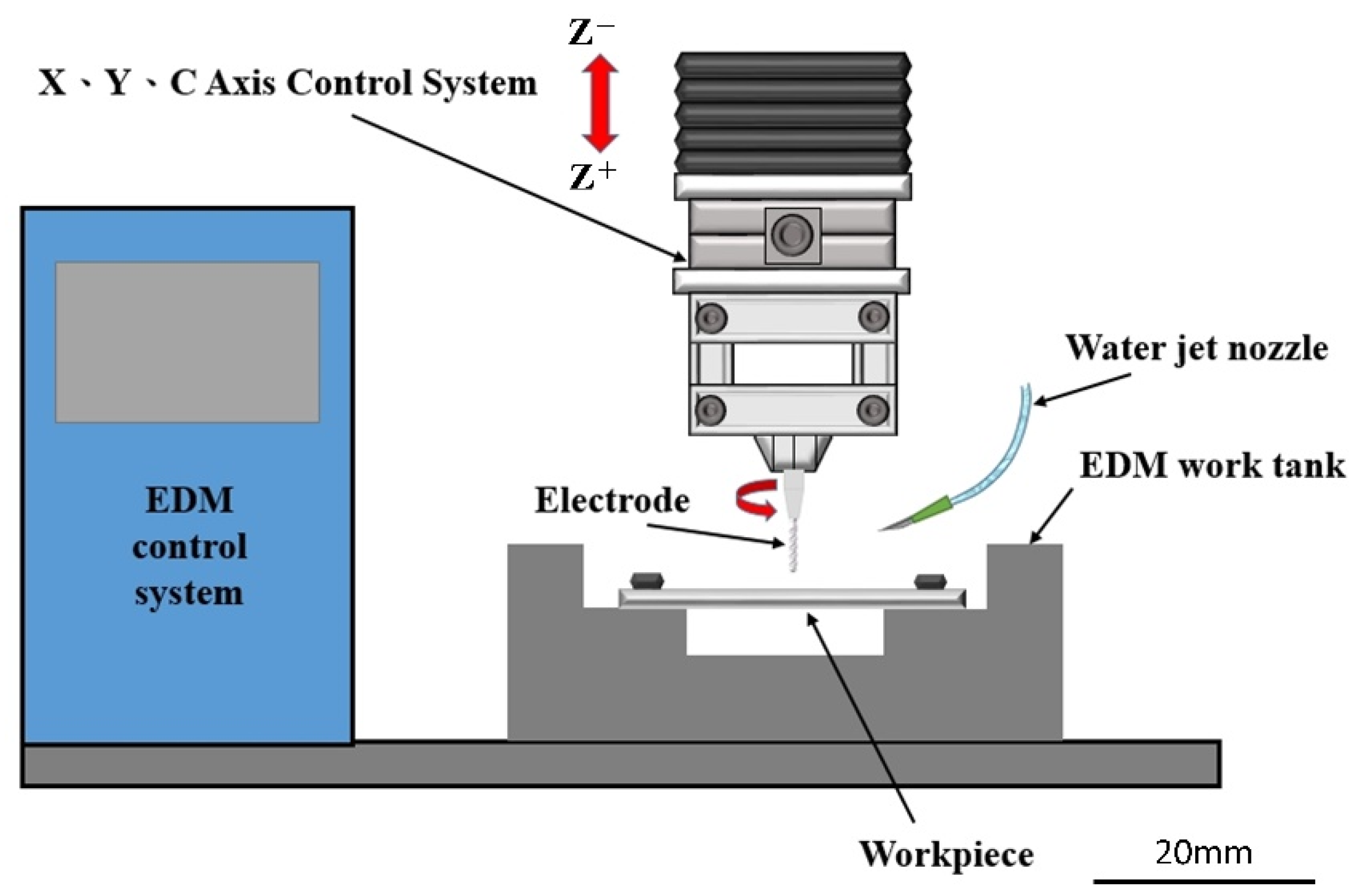
The µ-EDD was performed by using helical tool. The influence of processing parameters, including the pulse on time, gap voltage, duty factor, and spindle rotational speed on the micro hole machining accuracy, machining time, and electrode wear length, were investigated. The microscopic image measuring instrument is used to measure the electrode’s outer diameter and to observe the surface morphology. The microscopic image measuring instrument and the SEM were used to measure the hole size and to observe the surface morphology, respectively.
3.1.1. Influence of Pulse on Time on Micro Hole
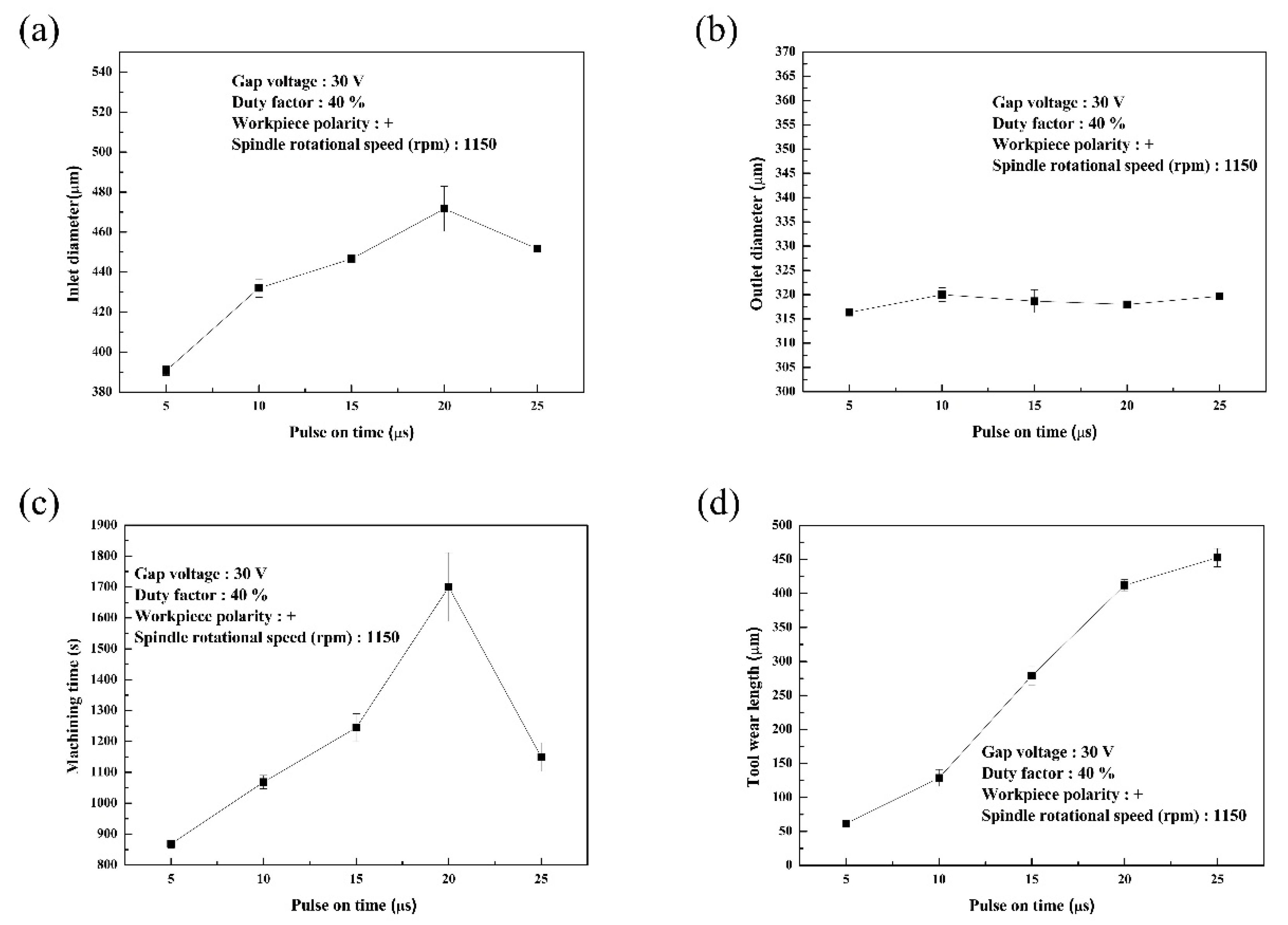
The relationship between pulse on time and inlet diameter is shown in
Figure 4a. When the pulse on time is 5 µs, the inlet diameter is 390 μm. The inlet diameter is 471 μm when the pulse on time is 20 µs, and the inlet diameter is larger than that at 5 µs by 17%. The discharge energy increased as the pulse on time increased. The phenomenon leads to large inlet diameter in the long pulse on time. The inlet diameter is decreased with the 25 µs pulse on time, because the brittle material would break during long-term exposure to high temperatures, causing the material to rupture and peel off. The existence of chips increased the chance of developing the electrical discharge phenomenon. The number of discharges increased. The inlet diameter and machining time of the µ-EDD are reduced. The inlet diameter is smaller and the surface morphology of the micro hole is better when the short pulse on time of 5 µs is used. The relationship between pulse on time and outlet diameter is shown in
Figure 4b. The trend of outlet diameter is relatively consistent with different pulse on time. The reason is that the electrode diameter decreases for high consumption under large discharge energy amounts.
The relationship between pulse on time and machining time is shown in
Figure 4c. When the pulse on time is 5 μs, the machining time is 868 s. As the pulse on time increases from 5 µs to 20 µs, the machining time increases to 1700 s. The machining time of the pulse on time of 20 µs increases by 48% at compared with the pulse on time of 5 µs. In the case of 5 µs pulse on time, the discharge energy density is relatively appropriate and the machining time is the lowest. The discharge energy increases with the pulse on time. It is likely to induce concentrated discharging phenomenon in high pulse on time. The concentrated discharging phenomenon facilitates the long machining time at a high pulse on time. When the pulse on time is 25 µs, the machining time is shortened. This is because the spall chips easily cause the electrical discharge phenomenon and increase the number of discharges.
The relation between the pulse on time and the length of tool wear is shown in
Figure 4d. The length of tool wear increases with the pulse on time. The discharge energy is increased with the pulse on time. The phenomenon facilitates a high length of tool wear in the long pulse on time.
Figure 5 shows the SEM image of the micro hole profile under different pulse on times. The SEM image shows that the overall discharged surface forms fine craters with the pulse on time of 5 µs. The surface morphology shows ruptured and spall craters with the pulse on time of 25 µs. Higher pulse on time will cause energy accumulation, which produce larger craters [
23].
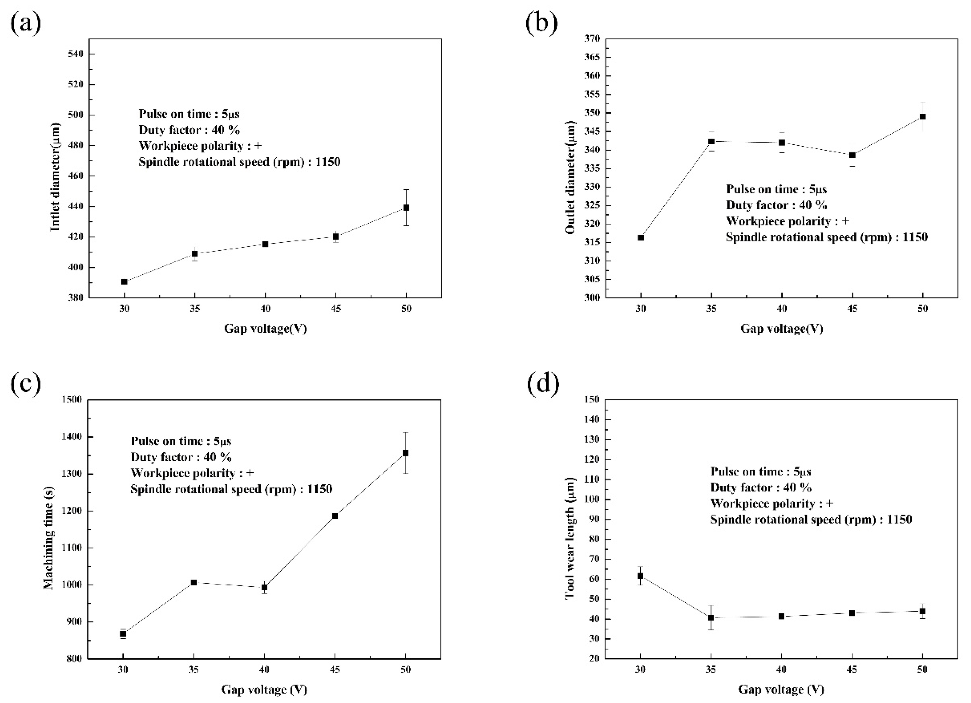
3.1.2. Influence of Gap Voltage on Micro Hole
The relation between the gap voltage and inlet diameter is shown in
Figure 6a. When the gap voltage is 30 V, the inlet diameter is 390 μm. As the gap voltage increases from 30 V to 50 V, the inlet diameter is increased to 439 μm. The inlet diameter increases by 11% as compared to that under the condition of 30 V. The inlet diameter increases with gap voltage. The higher the gap voltage is, the longer the discharging column will be. This is because more electrons escape from the cathode and impact the neutral particles in the dielectric fluid at the high gap voltage. The phenomenon generates greater ionization effect. The more the electrons impact the work-piece (anode), the larger the inlet diameter and outlet diameter will be.
The relation between the gap voltage and outlet diameter is shown in
Figure 6b. When the gap voltage is 30 V, the outlet diameter is 316 μm. As the gap voltage increases from 30 V to 50 V, the outlet diameter increases to 349 μm. The outlet diameter is increased by 9% compared to that at a gap voltage of 30 V.
The relation between the gap voltage and machining time is shown in
Figure 6c. When the gap voltage is 30 V, the machining time is 868 s. As the gap voltage is increased from 30 V to 50 V, the machining time increases to 1356 s. The machining time increases by 36% as compared to the gap voltage of 30 V. The machining time increases with gap voltage. The relation between the gap voltage and the length of tool wear is shown in
Figure 6d. When the gap voltage is 30 V, the length of tool wear is 61 μm. The length of tool wear decreases as the gap voltage increases. When the gap voltage increases to 50 V, the wear decreases to 44 μm and the length of tool wear is reduced by 28% as compared to that at a gap voltage of 30 V. The higher gap voltage enlarges the gap between the tool and work-piece. The large gap easily removes the debris, resulting in less tool wear.
Figure 7 shows the SEM image of the micro hole profile under different gap voltages. In the processing with a high gap voltage, the overall discharge surface forms fine discharge craters. The reason is that the high gap voltage results in a large gap between the tool and work-piece. There is adequate space for discharging the debris generated by the µ-EDD process. The concentrated discharging phenomenon is less likely to form. The sidewall surface is unlikely to form ruptured and spalled craters due to high heat accumulation [
24].
3.1.3. Influence of Duty Factor on Micro Hole
The relation between the duty factor and inlet diameter is shown in
Figure 8a. When the duty factor is 20%, the inlet diameter is 434 μm. As the duty factor increases from 20% to 40%, the inlet diameter is decreased to 390 μm. The inlet diameter reduces by 10% as compared to the condition of 20%. The inlet diameter decreases as the duty factor increases. In the processing with the low duty factor, the material removal rate is low. The machining time shortens as the duty factor increases. The total discharging time of the low duty factor on the lateral side of the micro hole is longer than the total discharging time of the high duty factor. Therefore, the inlet diameter is increased during the processing with a low duty factor. The relation between the duty factor and outlet diameter is shown in
Figure 8b. The outlet diameter is increased when the duty factor is 20%, and the reason is the same as the inlet diameter.
The relation between duty factor and machining time is shown in
Figure 8c. When the duty factor is 20%, the required machining time is 3324 s. As the duty factor increases from 20% to 40%, the machining time is shortened to 868 s. The machining time reduces by 74% as compared to the duty factor of 20%. The machining time becomes longer as the duty factor decreases. The pulse on time is only 20% of the pulse period, meaning the pulse off time is much longer than the pulse on time. Therefore, the material removal rate is decreased due to the low discharge energy. The relation between the duty factor and the tool wear length is shown in
Figure 8d. Among the duty factor parameters, there is no significant change in the length of electrode wear.
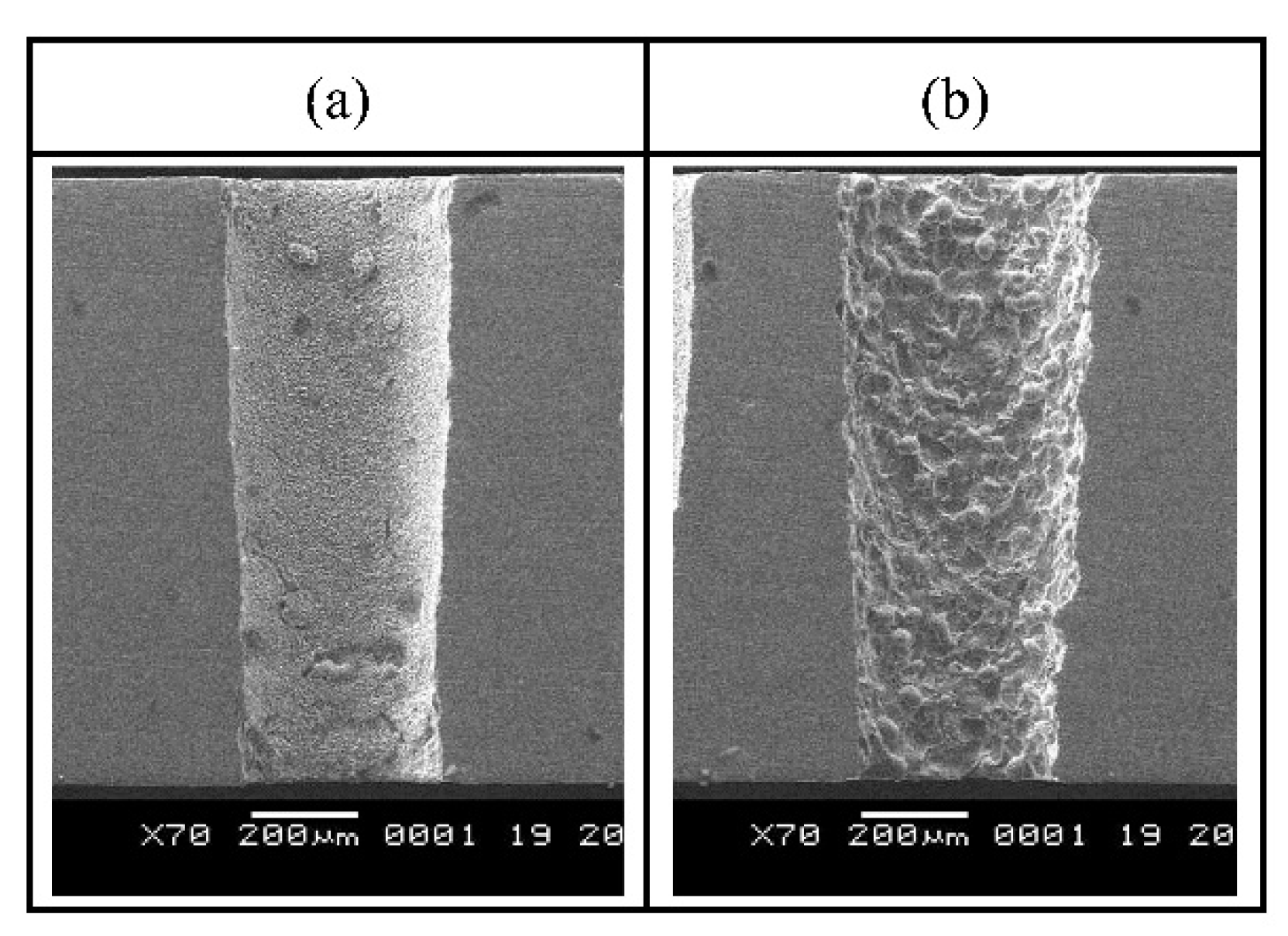
Figure 9 shows the SEM image of the micro hole profile under different duty factors. The overall discharged surface of a duty factor of 20% is worse than at a duty factor of 40%. The low duty factor results in increased lateral discharges and a longer machining time. The work piece material is likely to form ruptured and spall craters due to high heat accumulation at a duty factor of 20%, thus the surface morphology is worse.
3.1.4. Influence of Spindle Rotation Speed on Micro Hole
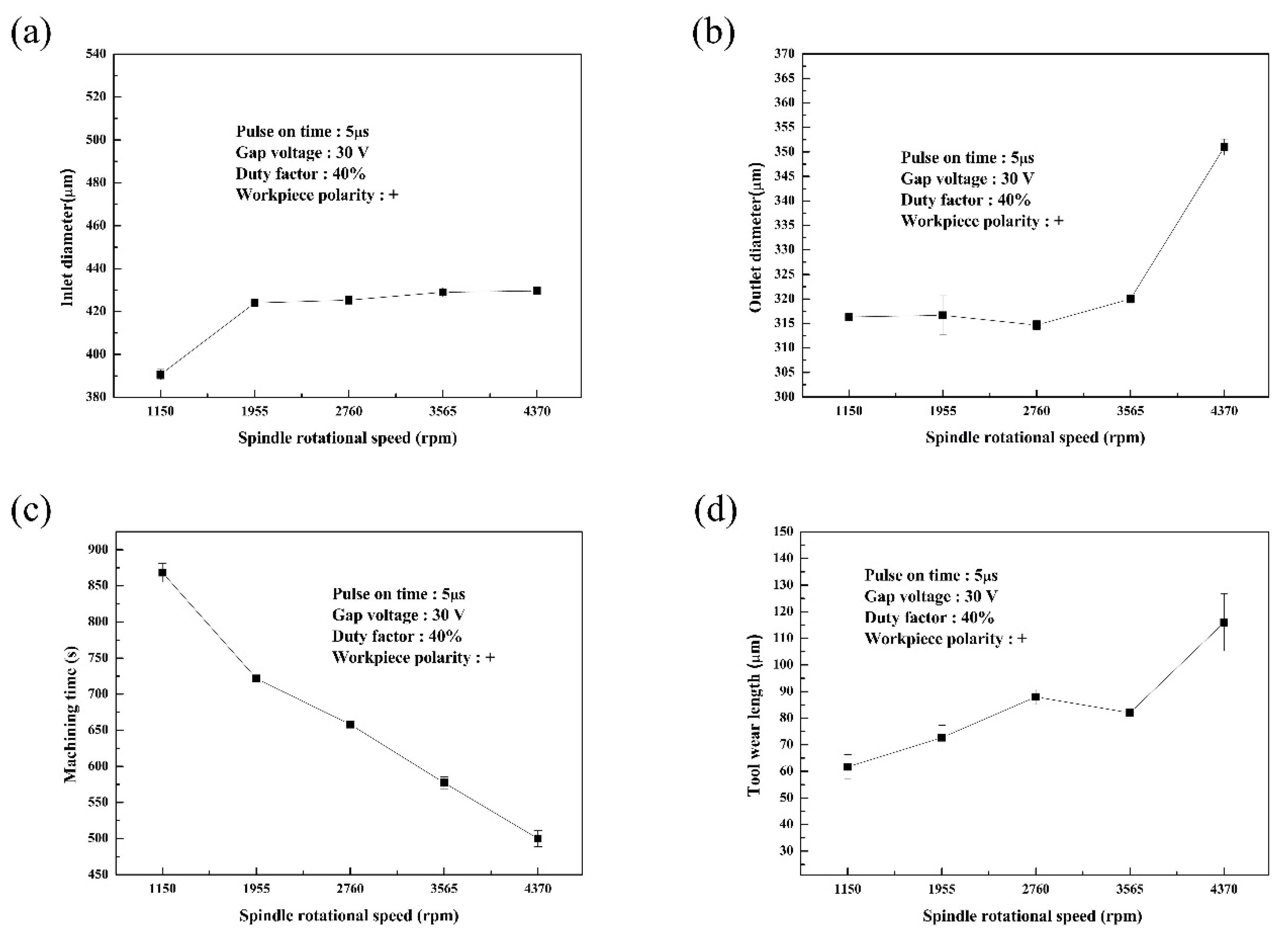
The relation between the spindle rotation speed and inlet diameter is shown in
Figure 10a. When the spindle rotation speed is 1150 rpm, the inlet diameter is 390 μm. As the electrode rotation speed is increased from 1150 rpm to 4370 rpm, the inlet diameter is increased to 429 μm. The inlet diameter increases by 9% as compared with that under the condition of 1150 rpm. As this experiment uses helical electrode as the experimental electrode, the area of the electrode side edge and tip sweeping the surface of the micro hole increases as the spindle rotation speed increases. Therefore, higher electrode rotation speed generates more discharges and discharge energy. The larger discharge energy increases the inlet diameter. However, the inlet diameter becomes stable when the spindle rotation speed is over 1955 rpm, because the hole gap is too large to discharge the sidewall of the micro hole. The relation between the spindle rotation speed and outlet diameter is shown in
Figure 10b. When the electrode rotation speed is 1150 rpm, the outlet diameter is 316 μm. As the electrode rotation speed increases from 1150 rpm to 4370 rpm, the outlet diameter increases to 351 μm, because higher spindle rotation speed can make the machining fluid circulate better. The outlet diameter is increased by 11% compared with that under the condition of 1150 rpm.
The relation between the spindle rotation speed and machining time is shown in
Figure 10c. When the spindle rotation speed is 1150 rpm, the machining time is 868 s. As the spindle rotation speed is increased from 1150 rpm to 4370 rpm, the machining time is shortened to 500 s. The machining time reduces by 42% as compared with that under the condition of 1150 rpm. The relation between the spindle rotation speed and the length of tool wear is shown in
Figure 10d. When the spindle rotation speed is 1150 rpm, the length of tool wear is 61 μm. When the spindle rotation speed is increased to 4370 rpm, the length of tool wear is increased to 116 μm. The length of tool wear increases by 47% as compared with that under the condition of 1150 rpm. The reason is that higher spindle rotation speed generates more discharges and discharge energy, resulting in increasing trend. When the discharge energy is increased, the machining time is decreased and the length of tool wear is increased.
Figure 11 shows the SEM image of the micro hole profile under different spindle rotation speed. As more discharges are generated at higher spindle rotation speeds, the overall discharged surface has severe molten accumulation and ruptured craters. The overall discharged surface at a spindle rotation speed of 4370 rpm is worse than that at a spindle rotation speed of 1150 rpm.
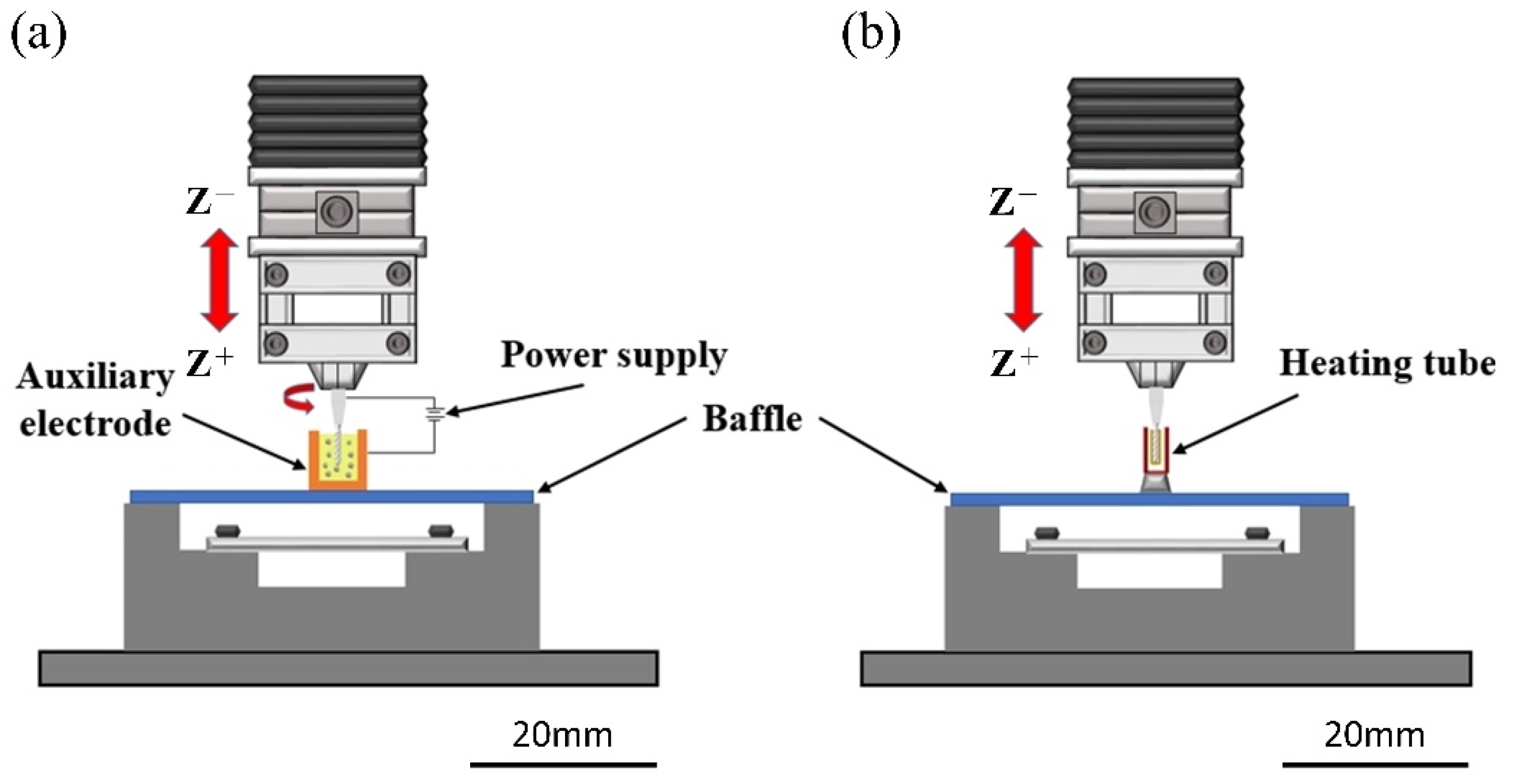
3.2. Experiments of Parameters of Electrophoretic Deposition Polishing
The helical tool is coated with SiC particles in a phenol formaldehyde resin solution and used as a polishing wheel by the EPD phenomenon after the µ-EDD experiments. The influence of the electrophoresis parameters, including the deposition time and coating voltage, on the diameter of the deposited tool after electrophoretic deposition are discussed. The feature and diameter of the EPD are observed and measured by using a microscopic image measuring instrument. The EPD polishing wheel was used to polish the inner surface of the electrical discharged micro hole. The SEM and the LSCM were used to observe and measure the shape of the micro holes’ inner walls and the surface roughness, respectively.
3.2.1. Influence of Deposition Time and Coating Voltage on EPD Polishing Wheel
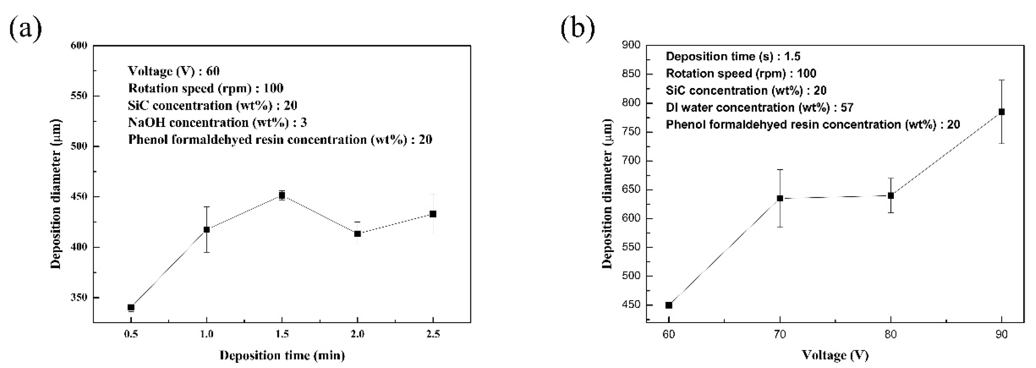
Figure 12a shows the relation between the deposition time and deposition diameter. When the deposition time increases to 1.5 min, the deposition diameter reaches the limit. The reason is that the helical tool (anode) is wrapped in SiC film. The SiC film formed an insulating barrier between the cathode and anode. Therefore, although the deposition time increases, the SiC powder deposition thickness on the helical tool does not continue to increase. The deposition diameter is 450 μm when the deposition time is 1.5 min; there is adequate diameter contact for the micro hole, thus the selected deposition time is 1.5 min.
According to
Figure 12b, the coating voltage is positively correlated with the SiC powder deposition thickness. The higher the coating voltage is, the larger the deposition diameter is. It is found in the previous experiments that the EPD polishing wheel with a larger deposition diameter became broken during the polishing process. Therefore, the selected coating voltage is 60 V. This is because the diameter of the micro hole is 390 μm after the µ-EDD process, and the deposition diameter of the polishing wheel is 450 μm. The EPD polishing wheel diameter has appropriate contact with the micro hole.
3.2.2. Discussion of the Polishing Results
The EPD polishing wheel was used to polish the inner surface of the electrical discharged micro hole. The constant parameters and setting values of the micro hole polishing experiment are shown in
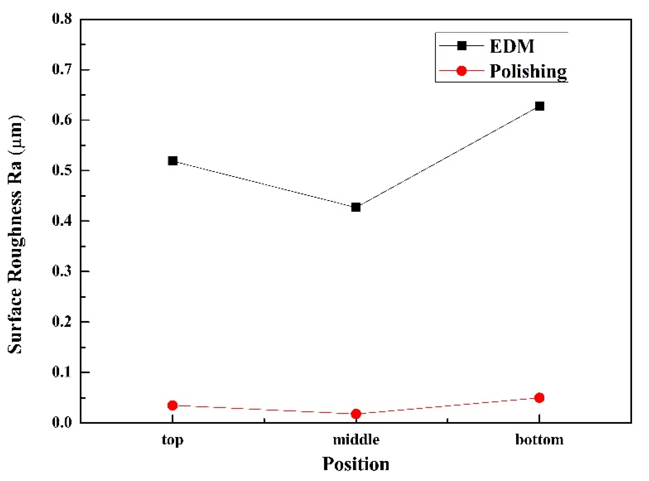
Table 6. The surface roughness of the inner surface of the micro hole is measured at three positions, which are the top position, the middle position, and the bottom position.
Figure 13 shows the relation between the measuring position and surface roughness. The surface roughness at the top position, the middle position and the bottom position are 0.519 μm, 0.427 μm and 0.628 μm, respectively, after the µ-EDD process. The surface roughness at the top position, the middle position, and the bottom position are 0.035 μm, 0.018 μm and 0.050 μm after the polishing experiment, respectively, which are lower than those of before polishing by 93%, 96% and 92%, respectively. The improvement is significant.
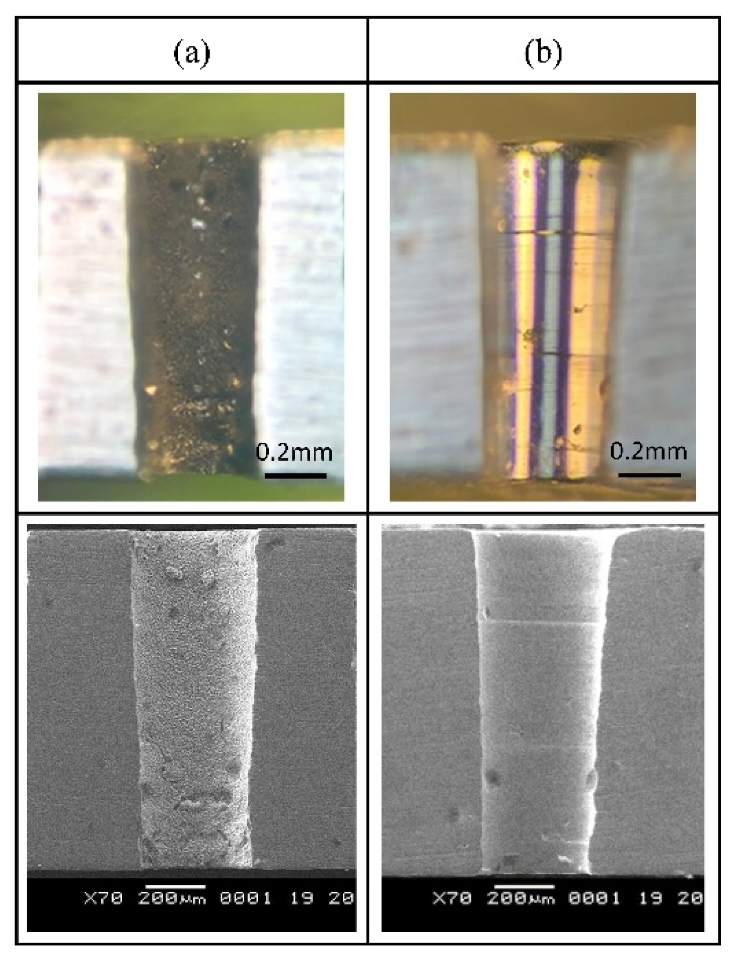
Figure 14 shows the photo and SEM images of the micro hole before and after polishing. The pores formed on the µ-EDD surface have been removed after polishing. The inner surface of the micro hole after polishing reached a mirror surface grade.


