Article

Microstructure and Magnetic Properties Dependence on the Sputtering Power and Deposition Time of TbDyFe Thin Films Integrated on Single-Crystal Diamond Substrate

1
School of Materials Science and Engineering, Anhui University of Science and Technology, Huainan 232001, China
2
Anhui International Joint Research Center for Nano Carbon-Based Materials and Environmental Health, Huainan 232001, China
*
Author to whom correspondence should be addressed.
These authors contributed equally to this work.
Processes 2022, 10(12), 2626; https://doi.org/10.3390/pr10122626
Submission received: 9 November 2022 / Revised: 30 November 2022 / Accepted: 5 December 2022 / Published: 7 December 2022

Abstract

:
As giant magnetostrictive material, TbDyFe is regarded as a promising choice for magnetic sensing due to its excellent sensitivity to changes in magnetic fields. To satisfy the requirements of high sensitivity and the stability of magnetic sensors, TbDyFe thin films were successfully deposited on single-crystal diamond (SCD) substrate with a Young’s modulus over 1000 GPa and an ultra-stable performance by radio-frequency magnetron sputtering at room temperature. The sputtering power and deposition time effects of TbDyFe thin films on phase composition, microstructure, and magnetic properties were investigated. Amorphous TbDyFe thin films were achieved under various conditions of sputtering power and deposition time. TbDyFe films appeared as an obvious boundary to SCD substrate as sputtering power exceeded 100 W and deposition time exceeded 2 h, and the thickness of the films was basically linear with the sputtering power and deposition time based on a scanning electron microscope (SEM). The film roughness ranged from 0.15 nm to 0.35 nm, which was measured by an atomic force microscope (AFM). The TbDyFe film prepared under a sputtering power of 100 W and a deposition time of 3 h possessed the coercivity of 48 Oe and a remanence ratio of 0.53, with a giant magnetostriction and Young’s modulus effect, suggesting attractive magnetic sensitivity. The realization of TbDyFe/SCD magnetic material demonstrates a foreseeable potential in the application of high-performance sensors.

Graphical Abstract

1. Introduction

Magnetic thin films deposited on various substrates are increasingly permeating through research fields of magnetic sensing [1,2], recording technology [3,4], photodetection [5,6,7,8,9], and microactuators [10,11,12,13], etc., due to its multiple-structure design. Inspired by the excellent mechanical, electrical, thermal, and chemical properties, diamond has attracted extraordinary interests as a substrate candidate for its extraordinary performance in fields such as microelectromechanical systems (MEMS) [14,15,16], electrical devices [17,18,19], and mechanical processing [20,21,22]. Rather than polycrystalline or nanocrystalline diamond, single-crystal diamond (SCD) demonstrates more comparable properties with ideal materials. Zhang et al. fabricated a highly sensitive MEMS magnetic sensor by using an SCD MEMS resonator integrated with giant magneto-strictive nano-thick FeGa thin film [23], and they studied the impact of growth parameters on FeGa thin film integrated with SCD substrate [24]. The soft magnetic properties of FeGa thin film deposited on SCD substrate proved to be superior to that on Si substate. TbDyFe ternary alloy is regarded as a promising choice in electronic engineering, especially for magnetic sensing in merits of its giant magnetostriction, high frequency bandwidth, high energy conversion rate, short response time, and high stability [25,26,27]. Recently, integrated TbDyFe thin film on SCD microcantilevers for magnetic sensing has been realized as an MEMS resonator structure via Young’s modulus effect [28]. Nevertheless, previous research was mainly devoted to the realization of unique function and outstanding performance, rather than illustrating how the processing condition of TbDyFe thin films deposited on SCD substrate affects the microstructure and magnetic properties. Conventionally, the processing condition plays a crucial role in the determination of the microstructure and magnetic properties of thin film, thus affecting the performance of devices [29,30,31,32]. Furthermore, the microstructure and magnetic properties of TbDyFe thin film on Si [33] and Pt/TiO2/SiO2/Si [34] substrate have proven to vary in strong dependence on the processing condition, including sputtering power, deposition pressure, substrate to target distance, and deposition temperature.
Herein, radio-frequency magnetron sputtering (RFMS) [35] was applied to obtain the TbDyFe thin films deposited on SCD substrates at room temperature via varying processing parameters involving sputtering power and deposition time. The impact of processing parameters on the phase composition, microstructure, and magnetic properties of TbDyFe thin films deposited on SCD substrate were investigated for the first time. A high dependence of surface roughness (Ra), coercivity (Hc), saturation magnetization (Hs), and remanence ratio (Mr/Ms) of TbDyFe thin films on the processing parameters was discussed in detail. This work provides a technical and theoretical basis for the magnetic property enhancement of TbDyFe films under various processing conditions and an integration with wide-gap semiconductor materials.

2. Materials and Methods

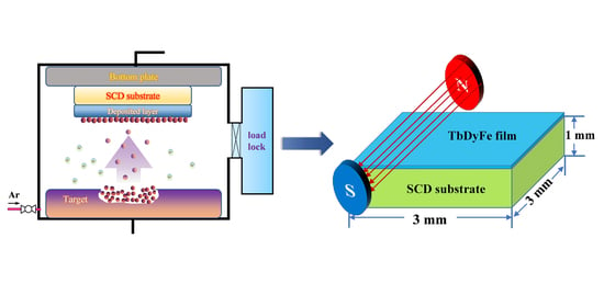
2.1. Fabrication and Treatment of SCD Substrates

Microwave plasma chemical vapor deposition (MPCVD, AX5200S) was employed to prepare high-quality (100)-oriented SCDs. Diamond seed crystals with a size of 3 mm × 3 mm × 1 mm were placed in the center of the growth chamber, and the growth temperature of diamond was monitored through infrared temperature measurement outside the chamber every half hour to ensure power stability. The SCD substrates were cleaned in the boiling mixture of nitric acid (69%, mass fraction) and sulfuric acid (98%, mass fraction) with a volume ratio of 1:2 at 300 °C for 120 min to remove surface hangings. Subsequently, the as-prepared SCD substrates were cleaned with acetone, ethanol, and deionized water, respectively, and then dried with a nitrogen gun.

2.2. Deposition of TbDyFe

TbDyFe possesses giant magnetostriction and stability as promising candidates integrated with SCD substrate for the fabrication of high-quality MEMS. Conventionally, processing parameters play an intensively important role in the influence on the phase composition, microstructure, and comprehensive properties of sputtered films.
TbDyFe thin films were deposited on to SCD substrate by RFMS using Tb0.3Dy0.7Fe1.92 alloy single harrow at room temperature. Herein, the distance between the target and the substrate was locked at 100 mm. The strain arising from the thermal expansion mismatch of the thin film and substrate was insignificant due to the room-temperature deposition. The growth chamber was vacuumed to below 10−6 Pa to guarantee the high-quality of TbDyFe thin films, and the working pressure was set to 0.8 Pa with 10 sccm Ar flow according to the result of the pre-experiment. A flexible sputtering power of 50–200 W with a step size of 50 W and deposition time of 1 h, 2 h, 3 h, and 4 h were varied to explore their effect on the morphology and performance of TbDyFe films. The varying processing parameters are exhibited in Table 1.

2.3. Characterization Method

The phase structures of SCD substrates were characterized by the aberration corrected transmission electron microscope (TEM, JEOL, Akishima, Japan, JEM-2100F(UHR), 200 kV) system using high-resolution TEM (HRTEM) and selected area electron diffraction (SAED). The as-processed specimen for TEM characterization was fabricated through the focused ion beam (FIB) method. Raman (HORIBA-Jobin-Yvon, Paris, France, T64000) technology was conducted to verify the quality of the SCD substrate. The crystal composition and thickness of prepared TbDyFe films were determined by X-ray diffraction (XRD, Rigaku Corporation, Tokyo, Japan, Smart lab, Cu Ka radiation (λ = 1.54 Å)) and a scanning electron microscope (SEM, Hitachi, Tokyo, Japan, S-4800), respectively, and film roughness was quantified by atomic force microscope (AFM, Bruker, Billerica, MA, USA, Nanoscope5). In-plane hysteresis loops were measured by a vibrating sample magnetometer (VSM, LakeShore, Columbus, OH, USA, 7410) with data normalized.

3. Results and Discussion

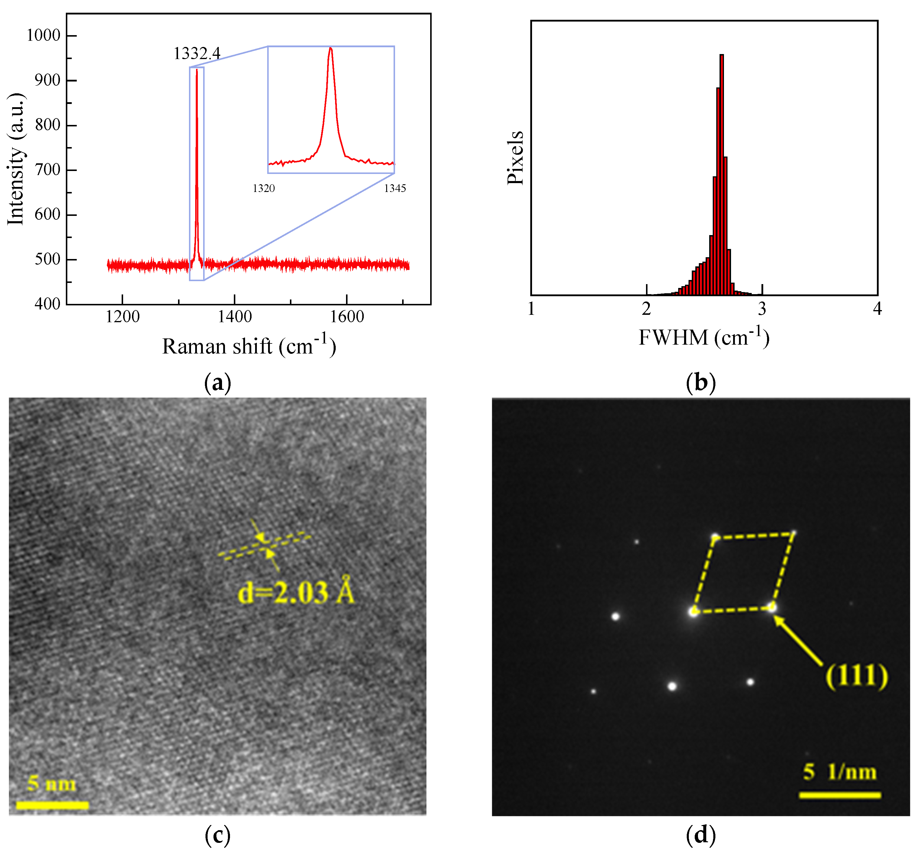
3.1. SCD Substrate Characterization

Raman spectroscopic characterization plays an irreplaceable role in the structural determination of carbon materials due to its advantages of having high resolution, having high sensitivity, being nondestructive, and having an easy operation [36,37]. The SCD constituted of sp3 hybridization possesses the Raman characteristic peak of 1332 cm−1 [24]. The Raman spectrum and full width at half maximum (FWHM) of the SCD substrate is exhibited in Figure 1a,b. As is shown, there is merely a sharp characteristic peak at 1332.4 cm−1, with FWHM distribution concentrated at 2.4–2.8 cm−1, which is exceedingly close to that of natural diamond. The high-resolution TEM image of the SCD substrate, as illustrated in Figure 1c, shows a complete and orderly diamond lattice structure, verifying its single crystal feature. The SAED image shown in Figure 1d further confirms the single crystal structure and high quality of SCD with a (111)-oriented lattice plane, which can act as ideal substrate material and provide a superior platform for the deposition of TbDyFe thin films.

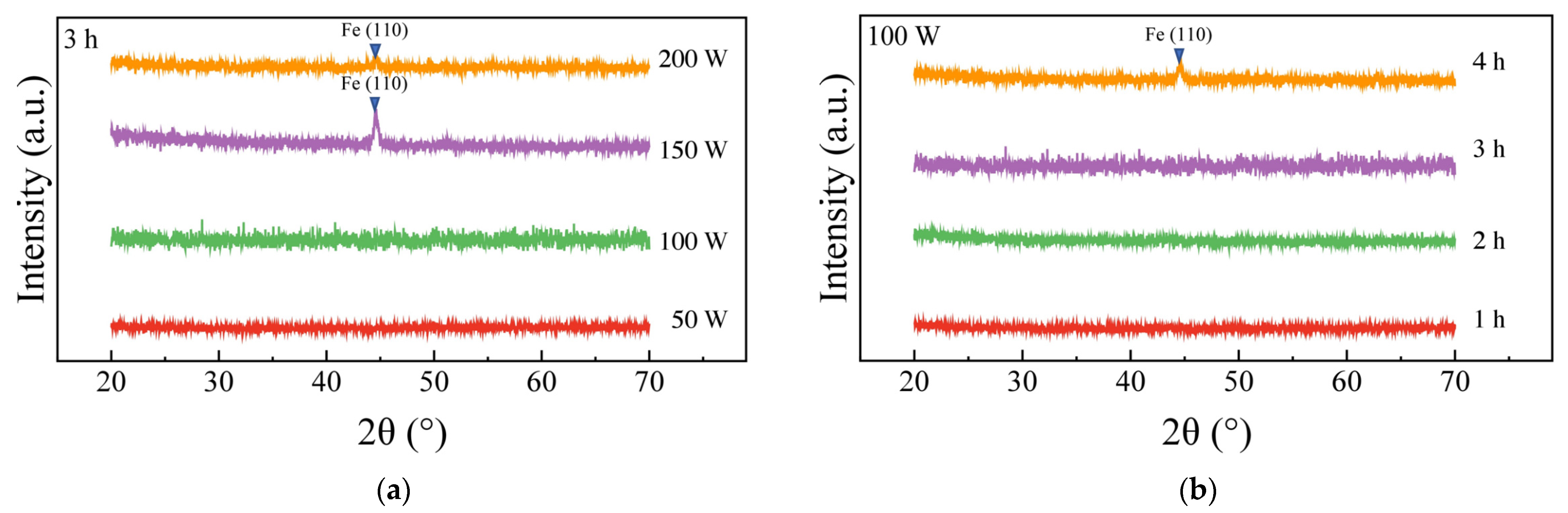
3.2. TbDyFe Phase Composition

Crystallized TbDyFe mainly consists of REFe2 (RE refers to Tb and Dy, Laves, cubic close packing (CCP)), which greatly contributes to the realization of larger magnetostriction coefficients. In order to reveal the crystal composition of TbDyFe thin film on SCD substrate, X-ray diffraction (XRD) was conducted. The XRD patterns of TbDyFe films prepared under 3 h and different sputtering powers are shown in Figure 2a, with no visible Laves phase characteristic peak, which can be attributed to that the films prepared at room temperature were basically amorphous [33,38], lacking long-range crystallographic order and producing inconspicuous peaks with low intensities in XRD patterns, according to Bragg’s law shown in Equation (1) [39,40].
= 2dhkl sin(θ)
where n is the order of diffraction, λ is the wavelength of the incident beam in nm, dhkl is the lattice spacing in nm, and θ is the angle of the diffracted beam in degree.
In addition, the characteristic peak of the Fe (110)-oriented texture perpendicular to the thin film plane appears as the sputtering power exceeds 150 W due to the obvious selective sputtering of Fe in the alloy target under excessive sputtering power. Generally, the broadening of the diffraction peak is mainly dictated by the grain size, not the internal strain, when the grain size is in the range of 0–100 nm. In this situation, the Scherrer equation, exhibited in Equation (2), is utilized to calculate the nanoscale grain size in out-of-plane direction based on XRD data [41].
D = 0.89λ/βcos(θ)
where D is the grain size in nm, λ is the X-ray wavelength in nm, θ is the diffraction angle in degree, and β is the FWHM in radian.
The grain size of Fe in the film at a sputtering power higher than 150 W was calculated as within 43 nm (shown in Table 2), indicating a smooth surface and good sputtering effect. As demonstrated in Figure 2b, XRD patterns of TbDyFe films obtained under 100 W and different deposition times from 1 to 4 h were still amorphous. At 4 h, the characteristic peak of Fe (110) occurred, presumably owing to the prolonged deposition time inducing a heated target and enlarging the energy of the system accordingly, hence the selective sputtering of Fe. As demonstrated in previous literature [25], different atomic mass leads to uneven deposition efficiency. The variety of surface composition induced by the increasing deposition time lasts until the new equilibrium is built in stable parameters. In this case, the proportion of RE and Fe atoms deposited on the substrate are approximate to those of the target.
As can be concluded from the XRD spectrum, high sputtering powers (150 W, 200 W) and long deposition times (4 h) both produce an iron diffraction peak owing to the selective sputtering of iron. The enrichment of iron atoms indicates that the composition distribution of sputtered films is uneven, which is not conducive to obtain TbDyFe films with a composition close to the target, thus degrading the magnetic performance. Therefore, a sputtering power of 100 W and a deposition time of 3 h are considered to be optimum conditions for sputtering at room temperature, which is verified by further characterization and analysis below.

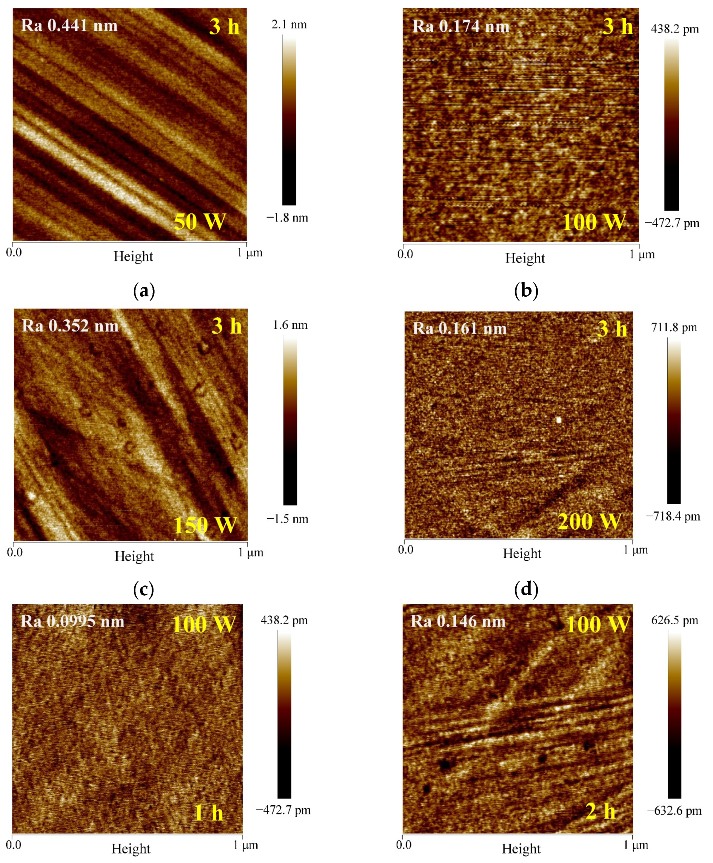
3.3. TbDyFe Microstructure

SEM images of TbDyFe thin film/SCD sample cross-section under 3 h and different sputtering powers are shown in Figure 3a–d. When the sputtered film vapor condenses on the diamond substrate, a large number of alloy target atoms appear randomly at first, and then the discontinuous distributed atoms continue to accumulate until they contact and merge with each other. A sputtering power of 50 W is too weak to form a distinct TbDyFe layer on the SCD surface until the power reaches 100 W. As was speculated, a small amount and low energy of Ar gas plasma in the working chamber induces inadequate sputtering of the alloy target atoms; accordingly, the films deposited on the substrate are almost invisible under the condition of excessively low sputtering power. Figure 3e–h are SEM images of TbDyFe thin film/SCD cross-section under 100 W and different deposition times. TbDyFe thin films and layer boundaries can be clearly observed despite 1 h, and the surfaces of the thin films are smooth without abnormal concavity.
Figure 4a–h exhibits the AFM images of TbDyFe films prepared under different sputtering powers (the same deposition time of 3 h) and various deposition times (the same sputtering power of 100 W). Further, the dependence of surface roughness Ra and film thickness on sputtering power and deposition time obtained by AFM and SEM, respectively, are shown in Figure 4i–j. A larger surface roughness of 0.441 nm of TbDyFe film was demonstrated as the sputtering power was 50 W, which can be attributed to the random and discontinuous distribution on the substrate effectuated by seldom alloy target atoms splashed out at low power. Additionally, the presence of fringes may be caused by the rough surface of single-crystalline diamond substrate. The roughness of the films fluctuated between 0.15 nm and 0.35 nm in parallel with the increase of sputtering power. The roughness of film fabricated under a sputtering power of 50 W was ignored due to its invisibility (shown in Figure 3a). The increase of roughness at 150 W was likely due to the selective sputtering of Fe, and the higher power improved the energy of the incoming ionized species and decreased the rearrangement time of the atoms on the substrate before the arrival of next atoms. At a higher power of 200 W, the kinetic energy of the incoming atoms increased, enhancing the lateral diffusion of Fe atoms, and then the surface roughness decreased. The variation rule of roughness along with power were consistent with the alteration of the XRD peak, as shown in Figure 2a. Furthermore, except for an operating power of 50 W, the deposition thickness of the films exhibited an approximately positive linear relationship with sputtering power but not significantly due to dissipation of substrate heating and secondary electron reflection at a high sputtering power (200 W). With the increase of deposition time, the films maintained dense and smooth surfaces with a maximum Ra of 0.243 nm. The roughness and thickness of the films had a linear positive correlation with the deposition time. The deposition rate of TbDyFe on SCD was around 30 nm-thick per hour.

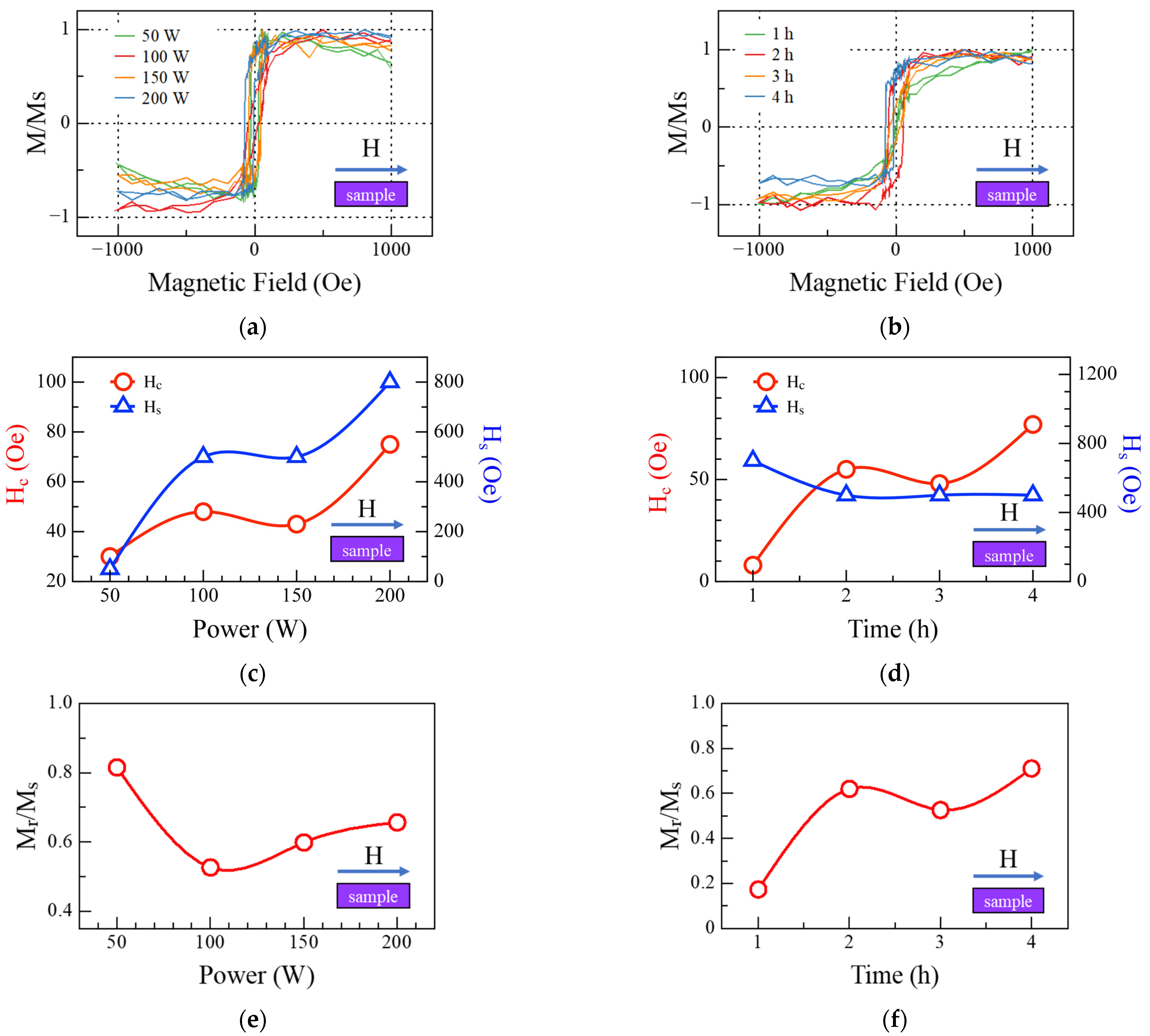
3.4. Magnetic Properties of TbDyFe

As shown in Figure 5a,b, the easy magnetization direction of the deposited TbDyFe films is in-plane. Since the films sputtered at 50 W were almost non-existent, their impact in the analysis was not taken into consideration. It can be seen from Figure 5c,e that there were minor discrepancies of in-plane Hc, Hs, and Mr/Ms between TbDyFe films acquired under a sputtering power of 100 W and 150 W, respectively, but they represented a sharp increase as the sputtering power reached 200 W. The roughness of the film was basically negatively correlated with Hc as the unobvious film thickness changed. For a film fabricated under 100 W, the Hc possessed an initial value of 48 Oe. As the sputtering power increased to 150 W and 200 W, the coercivity Hc decreased slightly to 43 Oe, and then increased to 75 Oe, while the Mr/Ms showed a steady increasing tendency. It was hypothesized that the effect originating from the surface roughness was more apparent for the thinner film. Defects occluded the movement of magnetic domain walls, increasing the coercivity of the film. This also explained that the saturated magnetic field strength of TbDyFe films acquired under a sputtering power of 100 W and 150 W, respectively, were identical, but the coercivity and remanence ratios were significantly different. Moreover, with increasing power, the intense collisions between various atoms on the target surface led to a temperature increase of the target and substrate, which could change both the micro morphology (lower roughness shown in Figure 4i) and stress, leading to the transformation of the film magnetic properties. As depicted in Figure 5d,f, the Hs of TbDyFe films had a weak dependence on the deposition time and remained at 500 Oe. Moreover, minuscule effects of the deposition time on Hc, Hs, and Mr/Ms of TbDyFe films were found as long as the deposition time was enough to form a continuous smooth film (>1 h) on the SCD substrate surface. With the lengthening of deposition time, Hc and Mr/Ms of TbDyFe films started at 55 Oe/0.62 and initially declined to 48 Oe/0.52, thereupon rising up to 77 Oe/0.71. As was speculated, the Hc of TbDyFe films was dominated by the film roughness when the deposition time was below 3 h. However, when the deposition time reached 4 h, the enhancement of Hc by deposition thickness occupied the main position. The appearance of the characteristic diffraction peak of Fe exhibited in Figure 2b increase the magnetic nonuniformity of the film, resulting in a decrease in the coercivity of the film [42]. It is worth noting that the excessively long sputtering time also increased the film surface temperature, thereby affecting the structure and magnetic properties of the film.

4. Conclusions

In summary, TbDyFe thin films integrated into the SCD substrate were successfully prepared by radio-frequency magnetron sputtering at ambient temperature. The sputtering power and deposition time exhibited significant influence on the phase composition, microstructure, and magnetic properties of TbDyFe thin films. Amorphous TbDyFe thin films were achieved with sputtering power from 100 to 200 W and deposition time exceeding 2 h. The thickness of the films was basically linear with the sputtering power and deposition time, and the film roughness fluctuated between 0.15 nm and 0.35 nm. The TbDyFe film prepared under a sputtering power of 100 W and a deposition time of 3 h possessed a coercivity of 48 Oe and a remanence ratio of 0.53, demonstrating attractive magnetic sensitivity.

Author Contributions

Conceptualization, Z.L. and X.S.; data curation, Y.Y.; formal analysis, C.L.; funding acquisition, Z.L. and X.S.; investigation, Y.K.; methodology, Z.L. and X.S.; project administration, Z.L. and X.S.; resources, Z.L. and X.S.; software, Y.C.; supervision, X.S.; validation, Z.L. and X.S.; visualization, J.Q.; writing—original draft, Z.L. and J.G.; writing—review and editing, X.S. All authors have read and agreed to the published version of the manuscript.

Funding

This research was funded by the Natural Science Research Projects of Anhui Universities, grant number KJ2020A0306; Anhui Provincial Natural Science Foundation, grant number 2208085QE171; Anhui International Joint Research Center for Nano Carbon-based Materials and Environmental Health, grant number NCMEH2022Y01; Scientific Research Foundation for High-level Talents of Anhui University of Science and Technology, grant number 13200411; The University Synergy Innovation Program of Anhui Province, GXXT-2022-083; and Huainan Science and Technology Project, grant number 2021078. The APC was funded by the Natural Science Research Projects of Anhui Universities, grant number KJ2020A0306 and Anhui Provincial Natural Science Foundation, grant number 2208085QE171.

Data Availability Statement

All data used to support this study are included within the article.

Conflicts of Interest

The authors declare no conflict of interest.

References

  1. Leung, C.M.; Li, J.; Viehland, D.; Zhuang, X. A review on applications of magnetoelectric composites: From heterostructural uncooled magnetic sensors, energy harvesters to highly efficient power converters. J. Phys. D Appl. Phys. 2018, 51, 263002. [Google Scholar] [CrossRef]
  2. Zhang, Z.; Sang, L.; Huang, J.; Chen, W.; Wang, L.; Takahashi, Y.; Mitani, S.; Koide, Y.; Koizumi, S.; Liao, M. Enhanced magnetic sensing performance of diamond MEMS magnetic sensor with boron-doped FeGa film. Carbon 2020, 170, 294–301. [Google Scholar] [CrossRef]
  3. Jang, J.; Choi, H.H.; Paik, S.H.; Kim, J.K.; Chung, S.; Park, J.H. Highly Improved Switching Properties in Flexible Aluminum Oxide Resistive Memories Based on a Multilayer Device Structure. Adv. Electron. Mater. 2018, 4, 1800355. [Google Scholar] [CrossRef]
  4. Lin, N.; Lin, Y.; Wu, G.; Chen, X.; Zhang, Z.; Hu, X.; Zhuang, N. Growth of high quality Si-based (Gd2Ce)(Fe4Ga)O12 thin film and prospects as a magnetic recording media. J. Alloys Compd. 2021, 875, 160086. [Google Scholar] [CrossRef]
  5. Jacob, A.A.; Balakrishnan, L.; Meher, S.R.; Shambavi, K.; Alex, Z.C. Structural, optical and photodetection characteristics of Cd alloyed ZnO thin film by spin coating. J. Alloys Compd. 2017, 695, 3753–3759. [Google Scholar] [CrossRef]
  6. Yu, M.; Gao, F.; Hu, Y.; Wang, L.; Hu, P.; Feng, W. Tunable electronic properties of multilayer InSe by alloy engineering for high performance self-powered photodetector. J. Colloid Interface Sci. 2020, 565, 239–244. [Google Scholar] [CrossRef]
  7. Li, Z.; Zhao, Y.; Li, W.; Peng, Y.; Zhao, W.; Wang, Z.; Shi, L.; Fei, W. A self-powered flexible UV-visible photodetector with high photosensitivity based on BiFeO3/XTiO3 (Sr, Zn, Pb) multilayer films. J. Mater. Chem. A 2022, 10, 8772–8783. [Google Scholar] [CrossRef]
  8. Shabbir, M.W.; Leuenberger, M.N. Theoretical Model of a Plasmonically Enhanced Tunable Spectrally Selective Infrared Photodetector Based on Intercalation-Doped Nanopatterned Multilayer Graphene. ACS Nano 2022, 16, 5529–5536. [Google Scholar] [CrossRef]
  9. Youngblood, N.; Chen, C.; Koester, S.J.; Li, M. Waveguide-integrated black phosphorus photodetector with high responsivity and low dark current. Nat. Photonics 2015, 9, 247–252. [Google Scholar] [CrossRef] [Green Version]
  10. Tan, Z.-Q.; Chen, Y.-C. Size-dependent electro-thermo-mechanical analysis of multilayer cantilever microactuators by Joule heating using the modified couple stress theory. Compos. Part B Eng. 2019, 161, 183–189. [Google Scholar] [CrossRef]
  11. Li, X.; Wang, Y.; Xu, B.; Zhou, X.; Men, C.; Tian, Z.; Mei, Y. Rolled-up single-layered vanadium oxide nanomembranes for microactuators with tunable active temperature. Nanotechnology 2019, 30, 354003. [Google Scholar] [CrossRef] [PubMed]
  12. Wei, Z.; Lo, C.; Liu, D.; Hsieh, Y.; Lee, Y.; Shiao, H.; Chiu, Y.; Lee, C.; Liao, C.; Chen, Y.; et al. Hysteresis in a Microactuator with Single-Domain Magnetic Thin Films. IEEE Trans. Magn. 2010, 46, 630–633. [Google Scholar] [CrossRef]
  13. Han, D.; Shinshi, T.; Azuma, N.; Kadota, S. An in-plane, large-stroke, multipole electromagnetic microactuator realized by guideways stacking mechanism. Sens. Actuators A Phys. 2019, 298, 111563. [Google Scholar] [CrossRef]
  14. Auciello, O.; Aslam, D.M. Review on advances in microcrystalline, nanocrystalline and ultrananocrystalline diamond films-based micro/nano-electromechanical systems technologies. J. Mater. Sci. 2021, 56, 7171–7230. [Google Scholar] [CrossRef]
  15. Shen, X.; Lv, Z.; Ichikawa, K.; Sun, H.; Sang, L.; Huang, Z.; Koide, Y.; Koizumi, S.; Liao, M. Stress effect on the resonance properties of single-crystal diamond cantilever resonators for microscopy applications. Ultramicroscopy 2022, 234, 113464. [Google Scholar] [CrossRef]
  16. Shen, X.; Wu, K.; Sun, H.; Sang, L.; Huang, Z.; Imura, M.; Koide, Y.; Koizumi, S.; Liao, M. Temperature dependence of Young’s modulus of single-crystal diamond determined by dynamic resonance. Diamond Relat. Mater. 2021, 116, 108403. [Google Scholar] [CrossRef]
  17. Yang, B.; Murooka, T.; Mizuno, K.; Kim, K.; Kato, H.; Makino, T.; Ogura, M.; Yamasaki, S.; Schmidt, M.E.; Mizuta, H.; et al. Vector Electrometry in a Wide-Gap-Semiconductor Device Using a Spin-Ensemble Quantum Sensor. Phys. Rev. Appl. 2020, 14, 044049. [Google Scholar] [CrossRef]
  18. Broadway, D.A.; Dontschuk, N.; Tsai, A.; Lillie, S.E.; Lew, C.T.K.; McCallum, J.C.; Johnson, B.C.; Doherty, M.W.; Stacey, A.; Hollenberg, L.C.L.; et al. Spatial mapping of band bending in semiconductor devices using in situ quantum sensors. Nat. Electron. 2018, 1, 502–507. [Google Scholar] [CrossRef]
  19. Masante, C.; Kah, M.; Hébert, C.; Rouger, N.; Pernot, J. Non-Volatile Photo-Switch Using a Diamond pn Junction. Adv. Electron. Mater. 2022, 8, 2100542. [Google Scholar] [CrossRef]
  20. Zhang, L. Filler metals, brazing processing and reliability for diamond tools brazing: A review. J. Manuf. Process. 2021, 66, 651–668. [Google Scholar] [CrossRef]
  21. Jin, T.; Ma, M.; Li, B.; Gao, Y.; Zhao, Q.; Zhao, Z.; Chen, J.; Tian, Y. Mechanical polishing of ultrahard nanotwinned diamond via transition into hard sp2-sp3 amorphous carbon. Carbon 2020, 161, 1–6. [Google Scholar] [CrossRef]
  22. Yue, Y.; Gao, Y.; Hu, W.; Xu, B.; Wang, J.; Zhang, X.; Zhang, Q.; Wang, Y.; Ge, B.; Yang, Z.; et al. Hierarchically structured diamond composite with exceptional toughness. Nature 2020, 582, 370–374. [Google Scholar] [CrossRef] [PubMed]
  23. Zhang, Z.; Wu, H.; Sang, L.; Huang, J.; Takahashi, Y.; Wang, L.; Imura, M.; Koizumi, S.; Koide, Y.; Liao, M. Single-crystal diamond microelectromechanical resonator integrated with a magneto-strictive galfenol film for magnetic sensing. Carbon 2019, 152, 788–795. [Google Scholar] [CrossRef]
  24. Zhang, Z.; Sang, L.; Huang, J.; Wang, L.; Koizumi, S.; Liao, M. Tailoring the magnetic properties of galfenol film grown on single-crystal diamond. J. Alloys Compd. 2021, 858, 157683. [Google Scholar] [CrossRef]
  25. Zhu, L.; Li, K.; Luo, Y.; Yu, D.; Wang, Z.; Wu, G.; Xie, J.; Tang, Z. Magnetostrictive properties and detection efficiency of TbDyFe/FeCo composite materials for nondestructive testing. J. Rare Earths 2019, 37, 166–170. [Google Scholar] [CrossRef]
  26. Wang, N.; Liu, Y.; Zhang, H.; Chen, X.; Li, Y. Effect of Co, Cu, Nb, Ti, V on magnetostriction and mechanical properties of TbDyFe alloys. Intermetallics 2018, 100, 188–192. [Google Scholar] [CrossRef]
  27. Dong, D.; Qian, J.; Huang, Y.; Shi, Y.; Tang, S.; Du, Y. Giant magnetostriction in TbDyFe/epoxy composites with spherical single-crystal particles. J. Alloys Compd. 2022, 917, 165558. [Google Scholar] [CrossRef]
  28. Shen, X.; Sun, H.; Sang, L.; Imura, M.; Koide, Y.; Koizumi, S.; Liao, M. Integrated TbDyFe Film on a Single-Crystal Diamond Microelectromechanical Resonator for Magnetic Sensing. Phys. Status Solidi RRL—Rapid Res. Lett. 2021, 15, 2100352. [Google Scholar] [CrossRef]
  29. Wang, J.; Kuang, S.; Yu, X.; Wang, L.; Huang, W. Tribo-mechanical properties of CrNbTiMoZr high-entropy alloy film synthesized by direct current magnetron sputtering. Surf. Coat. Technol. 2020, 403, 126374. [Google Scholar] [CrossRef]
  30. Basumatary, H.; Arout Chelvane, J.; Sridhara Rao, D.V.; Kamat, S.V.; Ranjan, R. Effect of sputtering parameters on the structure, microstructure and magnetic properties of Tb-Fe films. Thin Solid Film. 2015, 583, 1–6. [Google Scholar] [CrossRef]
  31. Ni, J.; Li, J.; Jian, J.; He, J.; Chen, H.; Leng, X.; Liu, X. Recent Studies on the Fabrication of Multilayer Films by Magnetron Sputtering and Their Irradiation Behaviors. Coatings 2021, 11, 1468. [Google Scholar] [CrossRef]
  32. Li, H.; Li, C.; Jia, H.; Chen, G.; Li, S.; Chen, K.; Wang, C.; Qiao, L. Facile fabrication of cordierite-based porous ceramics with magnetic properties. J. Adv. Ceram. 2022, 11, 1583–1595. [Google Scholar] [CrossRef]
  33. Mohanchandra, K.P.; Prikhodko, S.V.; Wetzlar, K.P.; Sun, W.Y.; Nordeen, P.; Carman, G.P. Sputter deposited Terfenol-D thin films for multiferroic applications. AIP Adv. 2015, 5, 097119. [Google Scholar] [CrossRef] [Green Version]
  34. More-Chevalier, J.; Cibert, C.; Domengès, B.; Ferri, A.; Desfeux, R.; Bouregba, R.; Poullain, G. Microstructure and magnetic properties dependence on the thickness of Tbx Dy1−x Fe2 thin films sputtered on Pt/TiO2/SiO2/Si substrate. Thin Solid Film. 2017, 623, 138–146. [Google Scholar] [CrossRef]
  35. Yan, J.; Wang, Y.; Wang, C.; Ouyang, J. Boosting energy storage performance of low-temperature sputtered CaBi2Nb2O9 thin film capacitors via rapid thermal annealing. J. Adv. Ceram. 2021, 10, 627–635. [Google Scholar] [CrossRef]
  36. Arenal, R.; Montagnac, G.; Bruno, P.; Gruen, D.M. Multiwavelength Raman spectroscopy of diamond nanowires present inn-type ultrananocrystalline films. Phys. Rev. B 2007, 76, 245316. [Google Scholar] [CrossRef]
  37. Long, D.A. Raman Spectroscopy; McGraw-Hill: New York, NY, USA, 1977; Volume 1. [Google Scholar]
  38. Lee, H.-S.; Cho, C. Study on advanced multilayered magnetostrictive thin film coating techniques for MEMS application. J. Mater. Process. Technol. 2008, 201, 678–682. [Google Scholar] [CrossRef]
  39. Epp, J. X-ray diffraction (XRD) techniques for materials characterization. In Materials Characterization Using Nondestructive Evaluation (NDE) Methods; Woodhead Publishing: Bremen, Germany, 2016; pp. 81–124. [Google Scholar]
  40. Rowe, M.C.; Brewer, B.J. AMORPH: A statistical program for characterizing amorphous materials by X-ray diffraction. Comput. Geosci. 2018, 120, 21–31. [Google Scholar] [CrossRef] [Green Version]
  41. Holzwarth, U.; Gibson, N. The Scherrer equation versus the ‘Debye-Scherrer equation’. Nat. Nanotechnol. 2011, 6, 534. [Google Scholar] [CrossRef]
  42. Liu, X.; Yang, Q.; Zhang, D.; Wu, Y.; Zhang, H. Magnetic properties of bismuth substituted yttrium iron garnet film with perpendicular magnetic anisotropy. AIP Adv. 2019, 9, 115001. [Google Scholar] [CrossRef]
Figure 1. (a) Raman spectrum, (b) full width at half maximum image, (c) high-resolution transmission electron microscope image, (d) selected area electron diffraction image of the SCD substrate.
Processes 10 02626 g001
Figure 2. XRD patterns of TbDyFe films obtained at different (a) sputtering powers (50 W, 100 W, 150 W, and 200 W) and (b) deposition times (1 h, 2 h, 3 h, and 4 h).
Processes 10 02626 g002
Figure 3. SEM images of TbDyFe film cross sections under different (ad) sputtering powers (50 W, 100 W, 150 W, and 200 W, respectively) and (eh) deposition times (1 h, 2 h, 3 h, and 4 h, respectively).
Processes 10 02626 g003
Figure 4. AFM images of TbDyFe thin films under diverse (ad) sputtering powers (50 W, 100 W, 150 W, and 200 W, respectively), (eh) deposition times (1 h, 2 h, 3 h, and 4 h); the dependence of surface roughness Ra and film thickness was on (i) sputtering power and (j) deposition time.
Processes 10 02626 g004aProcesses 10 02626 g004b
Figure 5. Sputtering power effect and deposition time effect on (a,b) in-plane hysteresis loop, (c,d) coercivity (Hc) and saturated magnetic field strength (Hs), and (e,f) the remanence ratio (Mr/Ms) of TbDyFe film.
Processes 10 02626 g005
Table 1. The varying processing parameters of TbDyFe thin films deposited on SCD substrate.
ThemeProcessing Parameters
Power (W)Time (h)Working Pressure (Pa)Ar Flow (sccm)
Power effect5030.810
100
150
200
Deposition time effect1001
2
3
4
Table 2. The grain size of Fe in the TbDyFe films calculated from the diffraction angle and FWHM.
Processing ParametersDiffraction Angle (°)FWHM (Radian)Grain Size (nm)
150 W, 3 h22.210.003542.34
200 W, 3 h22.250.008916.63
100 W, 4 h22.270.007918.87
Publisher’s Note: MDPI stays neutral with regard to jurisdictional claims in published maps and institutional affiliations.

